

Архив4 / Proshin_polnostyu_ves_kursach / DOC000301242(компаратор)
.pdf19-0194; Rev 1; 2/97
Ultra Low-Power, Low-Cost
Comparators with 2% Reference
_______________General Description
The MAX931-MAX934 single, dual, and quad micropower, low-voltage comparators plus an on-board 2% accurate reference feature the lowest power consumption available. These comparators draw less than 4µA supply current over temperature (MAX931), and include an internal 1.182V ±2% voltage reference, programmable hysteresis, and TTL/CMOS outputs that sink and source current.
Ideal for 3V or 5V single-supply applications, the MAX931-MAX934 operate from a single +2.5V to +11V supply (or a ±1.25V to ±5V dual supply), and each comparator’s input voltage range extends from the negative supply rail to within 1.3V of the positive supply.
The MAX931-MAX934’s unique output stage continuously sources as much as 40mA. And by eliminating powersupply glitches that commonly occur when comparators change logic states, the MAX931-MAX934 minimize parasitic feedback, which makes them easier to use.
The single MAX931 and dual MAX932/MAX933 provide a unique and simple method for adding hysteresis without feedback and complicated equations, using the HYST pin and two resistors.
For applications that require increased precision with similar power requirements, see the MAX921-MAX924 data sheet. These devices include a 1% precision reference.
|
INTERNAL |
COMPARATORS |
INTERNAL |
PACK- |
|
PART |
2% |
PER |
|||
HYSTERESIS |
AGE |
||||
|
REFERENCE |
PACKAGE |
|||
|
|
|
|||
|
|
|
|
|
|
|
|
|
|
8-Pin |
|
MAX931 |
Yes |
1 |
Yes |
DIP/SO/ |
|
|
|
|
|
µMAX |
|
|
|
|
|
|
|
|
|
|
|
8-Pin |
|
MAX932 |
Yes |
2 |
Yes |
DIP/SO/ |
|
|
|
|
|
µMAX |
|
|
|
|
|
|
|
|
|
|
|
8-Pin |
|
MAX933 |
Yes |
2 |
Yes |
DIP/SO/ |
|
|
|
|
|
µMAX |
|
|
|
|
|
|
|
MAX934 |
Yes |
4 |
No |
16-Pin |
|
DIP/SO |
|||||
|
|
|
|
||
|
|
|
|
|
________________________Applications
Battery-Powered Systems
Threshold Detectors
Window Comparators
Oscillator Circuits
Alarm Circuits
____________________________Features
♦Ultra-Low 4µA Max Quiescent Current Over Extended Temp. Range (MAX931)
♦Power Supplies:
Single +2.5V to +11V
Dual ±1.25V to ±5.5V
♦Input Voltage Range Includes Negative Supply
♦Internal 1.182V ±2% Bandgap Reference
♦Adjustable Hysteresis
♦TTL-/CMOS-Compatible Outputs
♦12µs Propagation Delay (10mV Overdrive)
♦No Switching Crowbar Current
♦40mA Continuous Source Current
♦Available in Space-Saving µMAX Package
______________Ordering Information
PART |
TEMP. RANGE |
|
PIN-PACKAGE |
|
|
|
|
MAX931CPA |
0°C to +70°C |
8 |
Plastic DIP |
|
|
|
|
MAX931CSA |
0°C to +70°C |
8 SO |
|
|
|
|
|
MAX931CUA |
0°C to +70°C |
8 |
µMAX |
MAX931EPA |
-40°C to +85°C |
8 |
Plastic DIP |
|
|
|
|
MAX931ESA |
-40°C to +85°C |
8 SO |
|
|
|
|
|
Ordering Information continued on last page.
For similar devices guaranteed over the military temp. range, see the MAX921-MAX924 data sheet. The MAX931, MAX933, and MAX934 are pin-compatible with the 1% accurate MAX921, MAX923, and MAX924, respectively. The MAX932 and MAX922 are not pin-compatible.
__________Typical Operating Circuit
VIN
|
|
7 |
|
3 |
IN+ |
V+ |
|
|
|
||
|
|
OUT |
8 |
4 |
IN- |
|
|
5 |
HYST |
|
|
6 |
REF |
MAX931 |
|
|
V- |
GND |
|
|
2 |
1 |
|
THRESHOLD DETECTOR
________________________________________________________________ Maxim Integrated Products 1
MAX934-MAX931
For free samples & the latest literature: http://www.maxim-ic.com, or phone 1-800-998-8800

MAX931-MAX934
Ultra Low-Power, Low-Cost Comparators with 2% Reference
ABSOLUTE MAXIMUM RATINGS
V+ to V-, V+ to GND, GND to V-................................ |
|
-0.3V, +12V |
Inputs |
|
|
Current, IN_+, IN_-, HYST............................................... |
|
20mA |
Voltage, IN_+, IN_-, HYST................ |
(V+ + 0.3V) to (V- – 0.3V) |
|
Outputs |
|
|
Current, REF.................................................................... |
|
20mA |
Current, OUT_ ................................................................. |
|
50mA |
Voltage, REF .................................... |
(V+ + 0.3V) to (V- – 0.3V) |
|
Voltage, OUT_ (MAX931/934) ..... |
(V+ + 0.3V) to (GND – 0.3V) |
|
Voltage, OUT_ (MAX932/933).......... |
(V+ + 0.3V) to (V- – 0.3V) |
|
OUT_ Short-Circuit Duration (V+ ≤ 5.5V) |
...............Continuous |
|
Continuous Power Dissipation (TA = +70°C) |
|
8-Pin Plastic DIP (derate 9.09mW/°C above +70°C) ... |
727mW |
8-Pin SO (derate 5.88mW/°C above +70°C)................ |
471mW |
8-Pin µMAX (derate 4.1mW/°C above +70°C) ............. |
330mW |
16-Pin Plastic DIP (derate 10.53mW/°C above +70°C)..842mW
16-Pin SO (derate 8.70mW/°C above +70°C) |
................696mW |
Operating Temperature Ranges: |
|
MAX93_C_ _ ....................................................... |
0°C to +70°C |
MAX93_E_ _..................................................... |
- 40°C to +85°C |
Storage Temperature Range ............................. |
- 65°C to +150°C |
Lead Temperature (soldering, 10sec) ............................. |
+300°C |
Stresses beyond those listed under “Absolute Maximum Ratings” may cause permanent damage to the device. These are stress ratings only, and functional operation of the device at these or any other conditions beyond those indicated in the operational sections of the specifications is not implied. Exposure to absolute maximum rating conditions for extended periods may affect device reliability.
ELECTRICAL CHARACTERISTICS—5V Operation
(V+ = 5V, V- = GND = 0V, TA = TMIN to TMAX, unless otherwise noted.)
PARAMETER |
|
CONDITIONS |
|
MIN |
TYP |
MAX |
UNITS |
|
|
|
|
|
|
|
|
|
|
POWER REQUIREMENTS |
|
|
|
|
|
|
|
|
|
|
|
|
|
|
|
|
|
Supply Voltage Range |
(Note 1) |
|
2.5 |
|
11 |
V |
||
|
|
|
|
|
|
|
|
|
|
|
MAX931, |
|
TA = +25°C |
|
2.5 |
3.2 |
|
|
|
|
|
|
|
|
|
|
|
|
HYST = REF |
|
C/E temp. ranges |
|
|
4 |
|
|
|
|
|
|
|
|
|
|
|
|
MAX932, |
|
TA = +25°C |
|
3.1 |
4.5 |
|
|
|
|
|
|
|
|
|
|
Supply Current |
IN+ = IN- + 100mV |
HYST = REF |
|
C/E temp. ranges |
|
|
6 |
µA |
|
|
|
|
|
|
|||
MAX933, |
|
TA = +25°C |
|
3.1 |
4.5 |
|||
|
|
|
|
|
||||
|
|
|
|
|
|
|
|
|
|
|
HYST = REF |
|
C/E temp. ranges |
|
|
6 |
|
|
|
|
|
|
|
|
|
|
|
|
MAX934 |
|
TA = +25°C |
|
5.5 |
6.5 |
|
|
|
|
|
|
|
|
|
|
|
|
|
C/E temp. ranges |
|
|
8.5 |
|
|
|
|
|
|
|
|
|
||
|
|
|
|
|
|
|
|
|
COMPARATOR |
|
|
|
|
|
|
|
|
|
|
|
|
|
|
|
|
|
Input Offset Voltage |
VCM = 2.5V |
|
|
|
±10 |
mV |
||
Input Leakage Current (IN-, IN+) |
IN+ = IN- = 2.5V, C/E temp. ranges |
|
±0.01 |
±5 |
nA |
|||
|
|
|
|
|
|
|
||
Input Leakage Current (HYST) |
MAX931, MAX932, MAX933 |
|
|
±0.02 |
|
nA |
||
|
|
|
|
|
|
|
|
|
Input Common-Mode Voltage Range |
|
|
|
|
V- |
|
V+ – 1.3 |
V |
|
|
|
|
|
|
|
|
|
Common-Mode Rejection Ratio |
V- to (V+ – 1.3V) |
|
|
0.1 |
1.0 |
mV/V |
||
|
|
|
|
|
|
|
||
Power-Supply Rejection Ratio |
V+ = 2.5V to 11V |
|
|
0.1 |
1.0 |
mV/V |
||
|
|
|
|
|
|
|
||
Voltage Noise |
100Hz to 100kHz |
|
|
20 |
|
µVRMS |
||
|
|
|
|
|
|
|
||
Hysteresis Input Voltage Range |
MAX931, MAX932, MAX933 |
|
REF – 0.05 |
|
REF |
V |
||
|
|
|
|
|
|
|
|
|
Response Time |
TA = +25°C, 100pF load |
|
Overdrive = 10mV |
|
12 |
|
µs |
|
|
|
|
|
|
||||
|
Overdrive = 100mV |
|
4 |
|
||||
|
|
|
|
|
|
|
||
|
|
|
|
|
|
|
|
|
2 _______________________________________________________________________________________

Ultra Low-Power, Low-Cost
Comparators with 2% Reference
ELECTRICAL CHARACTERISTICS—5V Operation (continued)
(V+ = 5V, V- = GND = 0V, TA = TMIN to TMAX, unless otherwise noted.)
PARAMETER |
CONDITIONS |
|
MIN |
TYP |
MAX |
UNITS |
|
|
|
|
|
|
|
|
|
Output High Voltage |
C/E temp. ranges, IOUT = 17mA |
|
V+ – 0.4 |
|
|
V |
|
|
|
|
|
|
|
|
|
|
|
|
MAX932, |
|
|
V- + 0.4 |
|
|
C/E temp. ranges, |
|
MAX933 |
|
|
|
|
Output Low Voltage |
|
|
|
|
V |
||
|
|
|
|
|
|||
IOUT = 1.8mA |
|
|
|
|
|
||
|
MAX931, |
|
GND + 0.4 |
||||
|
|
|
|
||||
|
|
|
MAX934 |
|
|
||
|
|
|
|
|
|
|
|
|
|
|
|
|
|
|
|
XREFERENCE |
|
|
|
|
|
|
|
Reference Voltage |
C temp. range |
|
1.158 |
1.182 |
1.206 |
V |
|
|
|
|
|
|
|
||
E temp. range |
|
1.147 |
|
1.217 |
|||
|
|
|
|
||||
|
|
|
|
|
|
|
|
Source Current |
TA = +25°C |
|
15 |
25 |
|
µA |
|
|
|
|
|
|
|
||
C/E temp. ranges |
|
6 |
|
|
|||
|
|
|
|
|
|||
|
|
|
|
|
|
|
|
Sink Current |
TA = +25°C |
|
8 |
15 |
|
µA |
|
|
|
|
|
|
|
||
C/E temp. ranges |
|
4 |
|
|
|||
|
|
|
|
|
|||
|
|
|
|
|
|
|
|
Voltage Noise |
100Hz to 100kHz |
|
|
100 |
|
µVRMS |
|
Note 1: MAX934 comparators work below 2.5V, see Low-Voltage Operation section for more details.
ELECTRICAL CHARACTERISTICS—3V Operation
(V+ = 3V, V- = GND = 0V, TA = TMIN to TMAX, unless otherwise noted.)
PARAMETER |
CONDITIONS |
|
MIN |
TYP |
MAX |
UNITS |
||
|
|
|
|
|
|
|
|
|
POWER REQUIREMENTS |
|
|
|
|
|
|
|
|
|
|
|
|
|
|
|
|
|
|
|
MAX931, |
|
TA = +25°C |
|
2.4 |
3.0 |
|
|
|
|
|
|
|
|
|
|
|
|
HYST=REF |
|
C/E temp. ranges |
|
|
3.8 |
|
|
|
|
|
|
|
|
||
|
|
|
|
|
|
|
|
|
|
|
MAX932, |
|
TA = +25°C |
|
3.4 |
4.3 |
|
Supply Current |
IN+ = (IN- + 100mV) |
HYST=REF |
|
C/E temp. ranges |
|
|
5.8 |
µA |
|
|
|
|
|
|
|||
|
|
MAX933, |
|
TA = +25°C |
|
3.4 |
4.3 |
|
|
|
HYST=REF |
|
C/E temp. ranges |
|
|
5.8 |
|
|
|
|
|
|
|
|
|
|
|
|
MAX934 |
|
TA = +25°C |
|
5.2 |
6.2 |
|
|
|
|
|
|
|
|
|
|
|
|
|
C/E temp. ranges |
|
|
8.0 |
|
|
|
|
|
|
|
|
|
||
|
|
|
|
|
|
|
|
|
COMPARATOR |
|
|
|
|
|
|
|
|
|
|
|
|
|
|
|
||
Input Offset Voltage |
VCM = 1.5V |
|
|
|
±10 |
mV |
||
Input Leakage Current (IN-, IN+) |
IN+ = IN- = 1.5V, C/E temp. ranges |
|
±0.01 |
±1 |
nA |
|||
|
|
|
|
|
|
|
||
Input Leakage Current (HYST) |
MAX931, MAX932, MAX933 |
|
|
±0.02 |
|
nA |
||
|
|
|
|
|
|
|
|
|
MAX934-MAX931
_______________________________________________________________________________________ 3

MAX931-MAX934
Ultra Low-Power, Low-Cost
Comparators with 2% Reference
ELECTRICAL CHARACTERISTICS—3V Operation (continued)
(V+ = 3V, V- = GND = 0V, TA = TMIN to TMAX, unless otherwise noted.)
PARAMETER |
CONDITIONS |
MIN |
TYP |
MAX |
UNITS |
||
|
|
|
|
|
|
|
|
Input Common-Mode Voltage Range |
|
|
|
V- |
|
V+ – 1.3 |
V |
|
|
|
|
|
|
|
|
Common-Mode Rejection Ratio |
V- to (V+ – 1.3V) |
|
0.2 |
1 |
mV/V |
||
|
|
|
|
|
|
||
Power-Supply Rejection Ratio |
V+ = 2.5V to 11V |
|
0.1 |
1 |
mV/V |
||
|
|
|
|
|
|
||
Voltage Noise |
100Hz to 100kHz |
|
20 |
|
µVRMS |
||
|
|
|
|
|
|
||
Hysteresis Input Voltage Range |
MAX931, MAX932, MAX933 |
REF – 0.05 |
|
REF |
V |
||
|
|
|
|
|
|
|
|
Response Time |
TA = +25°C, 100pF load |
Overdrive = 10mV |
|
14 |
|
µs |
|
|
|
|
|
||||
Overdrive = 100mV |
|
5 |
|
||||
|
|
|
|
|
|||
|
|
|
|
|
|
|
|
Output High Voltage |
C/E temp. ranges, IOUT = 10mA |
V+ – 0.4 |
|
|
V |
||
|
|
|
|
|
|
|
|
|
|
|
MAX932, |
|
|
V- + 0.4 |
|
|
|
|
MAX933 |
|
|
|
|
Output Low Voltage |
C/E temp. ranges, IOUT = 0.8mA |
|
|
|
V |
||
|
|
|
|
||||
MAX931 |
|
GND + 0.4 |
|||||
|
|
|
|
|
|||
|
|
|
|
|
|
|
|
REFERENCE |
|
|
|
|
|
|
|
|
|
|
|
|
|
|
|
Reference Voltage |
C temp. range |
1.158 |
1.182 |
1.206 |
V |
||
|
|
|
|
|
|
||
E temp. range |
1.147 |
|
1.217 |
||||
|
|
|
|||||
|
|
|
|
|
|
||
Source Current |
TA = +25°C |
15 |
25 |
|
µA |
||
|
|
|
|
|
|
||
C/E temp. ranges |
6 |
|
|
||||
|
|
|
|
||||
|
|
|
|
|
|
||
Sink Current |
TA = +25°C |
8 |
15 |
|
µA |
||
|
|
|
|
|
|
||
C/E temp. ranges |
4 |
|
|
||||
|
|
|
|
||||
|
|
|
|
|
|
|
|
Voltage Noise |
100Hz to 100kHz |
|
100 |
|
µVRMS |
||
4 _______________________________________________________________________________________

Ultra Low-Power, Low-Cost
Comparators with 2% Reference
__________________________________________Typical Operating Characteristics
(V+ = 5V, V- = GND, TA = +25°C, unless otherwise noted.)
|
|
|
|
|
OUTPUT VOLTAGE LOW |
|
|
|
|
|
OUTPUT VOLTAGE HIGH vs. |
|
|
|
|
|
|
REFERENCE OUTPUT VOLTAGE vs. |
|
|
|||||||||||||||||||||||||||||||
|
|
|
|
|
vs. LOAD CURRENT |
|
|
|
|
|
|
|
|
|
|
|
LOAD CURRENT |
|
|
|
|
|
|
|
|
|
|
|
OUTPUT LOAD CURRENT |
|
|
|
|
||||||||||||||||||
|
2.5 |
|
|
|
|
|
|
|
|
|
|
|
|
|
|
MAX921/4-TOC1 |
5.0 |
|
|
|
|
|
|
|
|
|
|
|
|
|
|
|
|
MAX921/924-TOC2 |
|
1.190 |
|
|
|
|
|
|
|
|
|
|
|
|
|
|
MAX921/924-TOC3 |
|
|
|
|
|
|
|
|
|
V+ = 5V |
|
|
|
|
|
|
|
|
|
|
|
|
|
|
|
|
|
|
|
|
|
|
|
|
|
|
|
|
|
|
|
|
|
|
|
|||||||
|
|
|
|
|
|
|
|
|
|
|
|
|
|
|
|
|
|
|
|
|
|
|
|
|
|
|
|
|
|
|
|
|
|
|
|
|
|
SINK |
|
|
|
|
|
|
|
||||||
|
|
|
|
|
|
|
|
|
|
|
|
|
|
|
|
4.5 |
|
|
V+ = 5V |
|
|
|
|
|
|
|
|
|
|
|
(V)VOLTAGE |
1.185 |
|
|
|
|
|
|
|
|
|
|
|
|
|||||||
|
|
|
|
|
|
|
|
|
|
|
|
|
|
|
|
|
|
|
|
|
|
|
|
|
|
|
|
|
|
|
|
|
|
|
|
|
|
|
|
|
|||||||||||
|
2.0 |
|
|
|
|
|
|
|
|
|
|
|
|
|
|
|
|
|
|
|
|
|
|
|
|
|
|
|
|
|
|
|
|
|
|
|
|
|
|
|
|
|
|
|
|
|
|
|
|
||
|
|
|
|
|
|
|
|
|
|
|
|
|
|
|
|
|
|
|
|
|
|
|
|
|
|
|
|
|
|
|
|
|
|
|
|
|
|
|
|
|
|
|
|
|
|
|
|
|
|||
|
|
|
|
|
|
|
|
|
|
|
|
|
|
|
|
4.0 |
|
|
|
|
|
|
|
|
|
|
|
|
|
|
|
|
|
|
1.180 |
|
|
|
|
|
|
|
|
|
|
|
|
|
|
|
|
|
|
|
|
|
|
|
|
|
|
|
|
|
|
|
|
|
|
|
|
|
|
|
|
|
|
|
|
|
|
|
|
|
|
|
|
|
|
|
|
|
|
|
|
|
|
|
|
|
|||
|
|
|
|
|
|
|
|
|
|
|
|
|
|
|
|
|
|
|
|
|
|
|
|
|
|
|
|
|
|
|
|
|
|
|
|
|
|
|
|
|
|
|
|
|
|
|
|
|
|
||
|
1.5 |
|
|
V+ = 3V |
|
|
|
|
|
|
|
|
|
|
|
|
|
|
|
|
|
|
|
|
|
|
|
|
|
|
|
|
|
|
|
|
|
|
|
|
|
|
|
SOURCE |
|
|
|
|
|||
V |
|
|
|
|
|
|
|
|
|
|
|
|
|
|
V |
3.5 |
|
|
|
|
|
|
|
|
|
|
|
|
|
|
|
|
|
OUTPUT |
1.175 |
|
|
|
|
|
|
|
|
|
|
|
|
|
|
|
|
|
|
|
|
|
|
|
|
|
|
|
|
|
|
|
|
|
|
|
|
|
|
|
|
|
|
|
|
|
|
|
|
|
|
|
|
|
|
|
|
|
|
|
|
|
|
||||||
(V) |
|
|
|
|
|
|
|
|
|
|
|
|
|
|
|
(V) |
|
|
|
|
|
|
|
|
|
|
|
|
|
|
|
|
|
|
|
|
|
|
|
|
|
|
|
|
|
|
|
|
|
||
OL |
|
|
|
|
|
|
|
|
|
|
|
|
|
|
|
OH |
3.0 |
|
|
|
|
|
|
|
|
|
|
|
|
|
|
|
|
|
|
1.170 |
|
|
|
|
|
|
|
|
|
|
|
|
|
|
|
|
1.0 |
|
|
|
|
|
|
|
|
|
|
|
|
|
|
|
|
|
|
|
|
|
|
|
|
|
|
|
|
|
|
|
|
REFERENCE |
|
|
|
|
|
|
|
|
|
|
|
|
|
|
|
||
|
|
|
|
|
|
|
|
|
|
|
|
|
|
|
|
|
|
|
|
|
|
|
|
|
|
|
|
|
|
|
|
|
|
|
|
|
|
|
|
|
|
|
|
|
|
|
|
||||
|
|
|
|
|
|
|
|
|
|
|
|
|
|
|
|
|
|
|
|
|
|
|
|
|
|
|
|
|
|
|
|
|
|
|
|
|
|
|
|
|
|
|
|
|
|
||||||
|
|
|
|
|
|
|
|
|
|
|
|
|
|
|
|
|
|
|
|
|
|
|
|
|
|
|
|
|
|
|
|
|
|
|
|
|
|
|
|
|
|
|
|
|
|
|
|
|
|
||
|
|
|
|
|
|
|
|
|
|
|
|
|
|
|
|
|
2.0 |
|
|
|
|
|
|
|
|
|
|
|
|
|
|
|
|
|
1.160 |
|
|
OR |
|
|
|
|
|
|
|
|
|
|
|||
|
|
|
|
|
|
|
|
|
|
|
|
|
|
|
|
|
2.5 |
|
|
|
|
|
|
|
|
|
|
|
|
|
|
|
|
|
|
1.165 |
|
|
|
|
|
|
|
|
|
|
|
|
|
|
|
|
0.5 |
|
|
|
|
|
|
|
|
|
|
|
|
|
|
|
|
|
|
|
|
|
|
|
|
|
|
|
|
|
V+ = |
3V |
|
|
|
|
|
|
V+ = 5V |
|
|
|
|
|
|
|
|
|
|
||
|
|
|
|
|
|
|
|
|
|
|
|
|
|
|
|
|
|
|
|
|
|
|
|
|
|
|
|
|
|
|
|
|
|
|
|
|
|
|
|
|
|
|
|
|
|
|
|||||
|
|
|
|
|
|
|
|
|
|
|
|
|
|
|
|
|
|
|
|
|
|
|
|
|
|
|
|
|
|
|
|
|
|
|
|
|
|
|
V+ = 3V |
|
|
|
|
|
|
|
|
|
|
||
|
0.0 |
|
|
|
|
|
|
|
|
|
|
|
|
|
|
|
1.5 |
|
|
|
|
|
|
|
|
|
|
|
|
|
|
|
|
|
|
1.155 |
|
|
|
|
|
|
|
|
|
|
|
|
|
|
|
|
|
|
|
|
|
|
|
|
|
|
|
|
|
|
|
|
|
|
|
|
|
|
|
|
|
|
|
|
|
|
|
|
|
|
|
|
|
|
|
|
|
|
|
|
|
|
|
|
|||
|
0 |
4 |
8 |
12 |
|
16 |
20 |
0 |
|
10 |
20 |
30 |
|
40 |
|
50 |
|
|
0 |
5 |
|
10 |
15 |
20 |
25 |
30 |
|||||||||||||||||||||||||
|
|
|
|
|
LOAD CURRENT (mA) |
|
|
|
|
|
|
|
|
|
LOAD CURRENT (mA) |
|
|
|
|
|
|
|
|
|
|
OUTPUT LOAD CURRENT (μA) |
|
|
|||||||||||||||||||||||
|
|
|
|
|
REFERENCE VOLTAGE |
|
|
|
|
|
|
|
|
MAX931 |
|
|
|
|
|
|
|
|
|
|
|
|
MAX932 |
|
|
|
|
|||||||||||||||||||||
|
1.22 |
|
|
|
vs. TEMPERATURE |
|
|
SUPPLY CURRENT vs. TEMPERATURE |
|
SUPPLY CURRENT vs. TEMPERATURE |
||||||||||||||||||||||||||||||||||||||||||
|
|
|
|
|
|
|
|
|
|
|
|
|
|
MAX921/924-TOC4 A)(CURRENTSUPPLYμ |
4.5 |
|
|
|
|
|
|
|
|
|
|
|
|
|
|
|
MAX921/924-TOC5 A)(CURRENTSUPPLYμ |
5.0 |
|
|
|
|
|
|
|
|
|
|
|
|
|
|
|
|
|
|
MAX921/924-TOC6 |
|
|
|
|
|
|
|
|
|
|
|
|
|
|
|
|
|
|
IN+ = IN- + 100mV |
|
|
|
|
|
|
|
|
|
|
|
|
|
|
|
|
|
|
|
|
|
|
|
|
|
|
|||||||||
(V)VOLTAGEREFERENCE |
1.16 |
|
|
|
|
|
|
|
|
|
|
|
|
|
|
|
|
|
|
|
|
|
|
|
|
IN+ = IN- +100mV |
|
|
|
|
|
|
|
|
|
|||||||||||||||||
|
|
|
|
|
|
|
|
|
|
|
|
|
|
|
|
|
|
|
|
|
|
|
|
|
|
|
|
|
|
|
|
|
|
|
|
|
|
|
|
|||||||||||||
|
1.21 |
|
|
|
|
|
|
|
|
|
|
|
|
|
|
4.0 |
|
|
|
|
|
|
|
|
|
|
|
|
|
|
|
|
4.5 |
|
|
|
|
|
|
|
|
|
|
|
|
|
|
|
|
|
|
|
|
1.20 |
|
|
EXTENDED TEMP. RANGE |
|
|
|
|
|
|
|
|
|
|
|
|
|
|
|
|
|
|
|
|
|
4.0 |
|
|
|
|
|
|
|
|
|
|
|
|
|
|
|
|
|
|
|
|||||||
|
|
|
|
|
|
|
|
|
|
|
|
|
|
|
|
|
|
|
|
|
|
|
|
|
|
|
|
|
|
|
|
|
|
|
|
|
|
|
|
|
|
|
|
|
|
|
|
|
|
|
||
|
|
|
|
|
|
|
|
|
|
|
|
|
|
|
|
|
|
|
|
|
|
|
|
|
|
|
|
|
|
|
|
|
|
|
|
|
|
|
|
|
|
|
|
|
|
|
|
|
|
|
|
|
|
|
|
|
|
|
|
|
|
|
|
|
|
|
|
|
|
|
|
V+ = 5V, V- = - 5V |
|
|
|
|
|
|
|
|
|
|
|
|
|
|
|
|
|
|
|
|
|
|
|
|
|
||||||||
|
1.19 |
|
|
|
|
COMMERCIAL |
|
|
|
|
|
|
3.5 |
|
|
|
|
|
|
|
|
|
|
|
|
|
|
|
|
|
|
|
|
|
|
|
|
|
|
|
|
|||||||||||
|
|
|
|
|
|
TEMP. RANGE |
|
|
|
|
|
|
|
|
|
|
|
|
|
|
|
|
|
|
|
|
|
|
|
|
|
|
|
|
|
|
|
|
|
|
|
|
|
|
|
|
|
|
|
|||
|
1.18 |
|
|
|
|
|
|
|
|
|
|
3.0 |
|
|
|
|
|
|
|
|
|
|
|
|
|
|
|
|
3.5 |
|
|
|
V+ = 5V, V- = 0V |
|
|
|
|
|
|
|
|
|||||||||||
|
|
|
|
|
|
|
|
|
|
|
|
|
|
|
|
|
|
|
|
|
|
|
|
|
|
|
|
|
|
|
|
|
|
|
|
|
|
|
|
|
|
|||||||||||
|
|
|
|
|
|
|
|
|
|
|
|
|
|
|
|
|
|
|
|
|
|
|
|
|
|
|
|
|
|
|
|
|
|
|
|
|
|
|
|
|
|
|
|
|
|
|
|
|
|
|||
|
|
|
|
|
|
|
|
|
|
|
|
|
|
|
|
|
|
|
|
|
|
|
|
|
|
|
|
|
|
|
|
|
|
|
|
|
|
|
|
|
|
|
|
|
|
|
|
|
|
|||
|
1.17 |
|
|
|
|
|
|
|
|
|
|
|
|
|
|
|
|
|
|
|
|
|
|
|
|
|
|
|
|
|
|
3.0 |
|
|
|
|
|
|
|
|
|
|
|
|
|
|
|
|
|
|
|
|
|
|
|
|
|
|
|
|
|
|
|
|
|
|
|
|
|
|
|
|
|
|
|
|
|
|
|
|
|
|
|
|
|
|
|
|
|
|
|
|
|
|
|
|
|
|
|
|
|
|
|||
|
|
|
|
|
|
|
|
|
|
|
|
|
|
|
2.5 |
|
|
|
|
|
|
|
|
|
|
V+ = 3V, V- = 0V |
|
|
|
|
|
|
|
|
|
|
|
|
|
|
|
|
|
|
|
|
||||||
|
|
|
|
|
|
|
|
|
|
|
|
|
|
|
|
|
|
|
|
|
|
|
|
|
|
|
|
|
|
|
|
|
|
|
|
|
|
|
|
|
|
|
|
|
|
|||||||
|
1.15 |
|
|
|
|
|
|
|
|
|
|
|
|
|
|
|
|
|
|
|
|
|
|
|
|
|
|
|
|
|
|
2.5 |
|
|
|
|
|
|
|
|
|
|
|
|
|
|
|
|
|
|
|
|
|
|
|
|
|
|
|
|
|
|
|
|
|
|
|
|
|
|
|
|
|
|
|
|
|
|
|
|
|
|
|
|
|
|
|
|
|
|
|
|
|
|
|
|
|
|
|
|
|
|
|||
|
|
|
|
|
|
|
|
|
|
|
|
|
|
|
|
|
|
|
|
|
|
|
|
|
|
|
|
|
|
|
|
|
|
|
|
|
|
|
|
|
|
|
|
|
|
|
|
|
|
|||
|
|
|
|
|
|
|
|
|
|
|
|
|
|
|
|
|
|
|
|
|
|
|
|
|
|
|
|
|
|
|
|
|
|
|
|
|
|
|
|
|
|
|
|
|
|
|
|
|
|
|
||
|
|
|
|
|
|
|
|
|
|
|
|
|
|
|
|
|
|
|
|
|
|
|
|
|
|
|
|
|
|
|
|
|
|
|
|
|
|
|
V+ = 3V, V- = 0V |
|
|
|
|
|
|
|||||||
|
1.14 |
|
|
|
|
|
|
|
|
|
|
|
|
|
|
2.0 |
|
|
|
V+ = 5V, V- = 0V |
|
|
|
|
|
|
|
2.0 |
|
|
|
|
|
|
|
|
|
|
|
|
||||||||||||
|
|
|
|
|
|
|
|
|
|
|
|
|
|
|
|
|
|
|
|
|
|
|
|
|
|
|
|
|
|
|
|
|
|
|
|
|
|
|
|
|
|
|
|
|
|
|
|
|
|
|||
|
|
|
|
|
|
|
|
|
|
|
|
|
|
|
|
|
|
|
|
|
|
|
|
|
|
|
|
|
|
|
|
|
|
|
|
|
|
|
|
|
|
|
|
|
|
|
|
|
|
|||
|
|
|
|
|
|
|
|
|
|
|
|
|
|
|
-60 |
-20 |
20 |
|
60 |
|
100 |
140 |
-60 |
-20 |
20 |
|
|
60 |
|
|
100 |
140 |
||||||||||||||||||||
|
-60 -40 |
-20 0 20 40 60 80 100 120 140 |
|
|
|
|
|
|
||||||||||||||||||||||||||||||||||||||||||||
|
|
|
|
|
|
|
TEMPERATURE (°C) |
|
|
|
|
|
|
|
|
|
|
TEMPERATURE (°C) |
|
|
|
|
||||||||||||||||||||||||||||||
|
|
|
|
|
TEMPERATURE (°C) |
|
|
|
|
|
|
|
|
|
|
|
|
|
|
|
|
|
|
|
|
|
||||||||||||||||||||||||||
|
|
|
|
|
|
|
|
|
|
|
|
|
|
|
|
|
|
|
|
|
|
|
|
|
|
|
|
|
|
|
MAX934 |
|
|
|
|
|||||||||||||||||
|
|
|
|
|
|
MAX933 |
|
|
|
|
|
|
|
|
MAX934 |
|
|
|
|
|
|
|
|
|
|
|
|
|
|
|
|
|||||||||||||||||||||
|
|
|
|
|
|
|
|
|
|
|
|
|
|
|
|
|
|
|
|
|
|
|
SUPPLY CURRENT vs. |
|
|
|||||||||||||||||||||||||||
|
|
SUPPLY CURRENT vs. TEMPERATURE |
|
|
SUPPLY CURRENT vs. TEMPERATURE |
|
|
|
|
LOW SUPPLY VOLTAGES |
|
|
||||||||||||||||||||||||||||||||||||||||
A)(μ |
5.0 |
|
|
|
|
MAX921/924-TOC7 |
A)(μ |
10 |
IN+ = (IN- + 100mV) |
|
|
MAX921/924-TOC8 |
A)(μ |
10 |
|
|
MAX921/924-TOC9 |
||
|
IN+ = IN- +100mV |
|
|
8 |
|
|
|
IN+ = IN- +100mV |
|
||||||||||
|
|
|
|
|
|
|
|
|
|
|
|
|
|
||||||
|
|
|
|
|
|
9 |
|
|
|
|
|
|
|
|
|
|
|||
|
4.5 |
|
|
|
|
|
|
|
|
|
|
|
|
|
|
|
|
|
|
|
|
|
|
|
|
|
|
|
|
|
|
|
|
|
|
|
|
|
|
CURRENT |
4.0 |
|
|
|
|
|
CURRENT |
|
|
|
|
|
|
|
CURRENT |
1 |
|
|
|
|
V+ = 5V, V- = 0V |
|
|
7 |
V+ = 5V, V- = -5V |
|
|
|
|
|
|
|
|||||||
|
|
|
|
|
|
|
|
|
|
|
|
|
|||||||
|
3.5 |
|
|
|
|
|
|
|
|
|
|
|
|
|
|
|
|||
|
|
|
|
|
|
|
6 |
|
|
|
|
|
|
|
|
|
|
|
|
SUPPLY |
|
|
|
|
|
|
SUPPLY |
|
|
|
|
|
|
SUPPLY |
|
|
|
|
|
3.0 |
|
|
|
|
|
5 |
|
|
|
V+ = 5V, V- = 0V |
|
0.1 |
|
|
|
||||
|
|
|
|
|
|
|
|
|
|
|
|
|
|
|
|||||
|
|
|
|
|
|
|
|
|
|
|
|
|
|
|
|
|
|||
|
2.5 |
|
V+ = 3V, V- = 0V |
|
|
|
4 |
|
|
V+ = 3V, V- = 0V |
|
|
|
|
|
|
|
||
|
|
|
|
|
|
|
|
|
|
|
|
|
|
|
|
|
|
||
|
2.0 |
|
|
60 |
|
|
|
3 |
-60 |
-20 |
20 |
60 |
100 |
140 |
|
0.01 |
|
|
|
|
-60 |
-20 |
20 |
100 |
140 |
|
|
|
1.0 |
1.5 |
2.0 |
2.5 |
|||||||
|
|
|
TEMPERATURE (°C) |
|
|
|
|
|
|
TEMPERATURE (°C) |
|
|
|
|
SINGLE-SUPPLY VOLTAGE (V) |
|
|||
MAX934-MAX931
_______________________________________________________________________________________ 5
MAX931-MAX934
Ultra Low-Power, Low-Cost
Comparators with 2% Reference
____________________________Typical Operating Characteristics (continued)
(V+ = 5V, V- = GND, TA = +25°C, unless otherwise noted.)
|
|
|
|
|
HYSTERESIS CONTROL |
|
|
|
|
|
|
|
|
|
TRANSFER FUNCTION |
|
|
|
|
|
|
|
RESPONSE TIME vs. |
|
|
|
|
||||||||||||||||||||||||
|
|
|
|
|
|
|
|
|
|
|
|
|
|
|
|
|
|
|
|
|
LOAD CAPACITANCE |
|
|
|
|
||||||||||||||||||||||||||
|
80 |
|
|
|
|
|
|
|
|
|
|
|
|
|
MAX921/924TOC10 |
5.0 |
|
|
|
|
|
|
|
|
|
|
|
|
|
|
|
|
MAX921/924-TOC11 |
18 |
|
|
|
|
|
|
|
|
|
|
|
|
|
|
|
|
MAX921/924TOC12 |
|
60 |
|
|
|
|
|
|
|
|
|
|
|
|
|
4.5 |
|
|
|
|
|
|
|
100k |
|
|
|
V0 |
|
|
|
16 |
|
|
|
|
|
|
|
|
|
|
|
|
|
|
|
|
||||
|
|
|
|
|
|
|
|
|
|
|
|
|
|
|
|
|
|
|
|
|
|
|
|
|
|
|
|
|
|
|
|
|
|
|
|
|
|
|
|
|
|
||||||||||
|
|
|
OUTPUT |
HIGH |
|
|
|
|
|
|
|
|
|
|
|
|
|
|
|
|
|
|
|
|
|
|
|
|
|
|
|
||||||||||||||||||||
|
|
|
|
|
|
|
|
|
|
4.0 |
|
|
|
|
|
|
|
|
|
|
|
|
|
|
|
|
|
|
|
|
|
|
|
|
|
|
|
|
|
|
|
|
|||||||||
|
|
|
|
|
|
|
|
|
|
|
|
|
|
|
|
|
|
|
|
|
|
|
|
|
|
|
|
|
|
|
|
|
|
|
|
|
|
|
|
|
|
|
|
|
|
|
|
|
|
|
|
|
|
|
|
|
|
|
|
|
|
|
|
|
|
|
|
|
|
|
|
|
|
|
|
|
|
|
|
|
|
|
|
|
|
|
|
|
|
|
|
|
|
|
|
|
|
|
|
|
|
|
|
|
40 |
|
|
|
|
|
|
|
|
|
|
|
|
|
OUTPUTVOLTAGE (V) |
3.5 |
|
|
|
|
|
|
|
10μF |
|
|
|
|
|
|
|
RESPONSETIME (μs) |
14 |
|
|
|
|
|
|
|
|
|
|
|
|
|
|
|
|
|
|
IN+– IN- (V) |
20 |
|
|
|
|
|
|
|
|
|
|
|
|
|
|
|
|
|
|
|
|
|
|
|
|
|
|
|
|
|
12 |
|
|
|
|
|
|
|
VOHL |
|
|
|
|
|
|
||||||
|
|
|
|
|
|
|
|
|
|
|
|
|
1.5 |
|
|
|
|
|
|
|
|
|
|
|
|
|
|
|
|
|
|
|
|
|
|
|
|
VOLH |
|
|
|
|
|
|
|
|
|||||
|
0 |
|
|
|
|
|
|
|
|
|
|
|
|
|
|
3.0 |
|
|
|
|
|
|
|
|
|
|
|
|
|
|
|
|
|
|
|
|
|
|
|
|
|
|
|
|
|
|
|
|
|
|
|
|
|
|
|
|
|
|
|
NO |
CHANGE |
|
|
|
|
2.5 |
|
|
|
|
|
|
|
|
|
|
|
|
|
|
|
|
|
10 |
|
|
|
|
|
|
|
|
|
|
|
|
|
|
|
|
|
||
|
|
|
|
|
|
|
|
|
|
|
|
|
|
2.0 |
|
|
|
|
|
|
|
|
|
|
|
|
|
|
|
|
|
|
|
|
|
|
|
|
|
|
|
|
|
|
|
|
|
|
|
||
|
-20 |
|
|
|
|
|
|
|
|
|
|
|
|
|
|
|
|
|
|
|
|
|
|
|
|
|
|
|
|
|
|
|
8 |
|
|
|
|
|
|
|
|
|
|
|
|
|
|
|
|
|
|
|
|
|
|
|
|
|
|
|
|
|
|
|
|
|
|
|
|
|
|
|
|
|
|
|
|
|
|
|
|
|
|
|
|
|
|
|
|
|
|
|
|
|
|
|
|
|
|
||||
|
|
|
|
|
|
|
|
|
|
|
|
|
|
|
|
|
|
|
|
|
|
|
|
|
|
|
|
|
|
|
|
|
|
|
|
|
|
|
|
|
|
|
|
|
|
|
|
||||
|
-40 |
|
|
|
|
|
|
|
|
|
|
|
|
|
|
1.0 |
|
|
|
|
|
|
|
|
|
|
|
|
|
|
|
|
|
6 |
|
|
|
|
|
|
|
|
|
|
|
|
|
|
|
|
|
|
|
|
|
|
|
|
|
|
|
|
|
|
|
|
|
|
|
|
|
|
|
|
|
|
|
|
|
|
|
|
|
|
|
|
|
|
|
|
|
|
|
|
|
|
|
|
|
|
|||
|
-60 |
|
|
OUTPUT |
LOW |
|
|
|
|
|
|
|
|
|
|
|
|
|
|
|
|
|
|
|
|
|
|
|
|
|
|
4 |
|
|
|
|
|
|
|
|
|
|
|
|
|
|
|
|
|
||
|
|
|
|
|
|
|
|
|
|
|
|
|
|
|
0.5 |
|
|
|
|
|
|
|
|
|
|
|
|
|
|
|
|
|
|
|
|
|
|
|
|
|
|
|
|
|
|
|
|
|
|
||
|
|
|
|
|
|
|
|
|
|
|
|
|
|
|
|
|
|
|
|
|
|
|
|
|
|
|
|
|
|
|
|
|
|
|
|
|
|
|
|
|
|
|
|
|
|
|
|
||||
|
-80 |
|
|
|
|
|
|
|
|
|
|
|
|
|
|
|
|
|
|
|
|
|
|
|
|
|
|
|
|
|
|
|
|
|
|
|
|
|
|
|
|
|
|
|
|
|
|
|
|
|
|
|
|
|
|
|
|
|
|
|
|
|
|
|
|
|
|
|
|
|
|
|
|
|
|
|
|
|
|
|
|
|
|
|
|
|
|
|
|
|
|
|
|
|
|
|
|
|
|
|
|
||
|
|
|
|
|
|
|
|
|
|
|
|
|
|
|
0 |
|
|
|
|
|
|
|
|
|
|
|
|
|
|
|
|
|
2 |
|
|
|
|
|
|
|
|
|
|
|
|
|
|
|
|
|
|
|
0 |
10 |
20 |
30 |
40 |
50 |
|
-0.3 -0.2 -0.1 |
|
0 |
0.1 |
0.2 0.3 |
0 |
20 |
40 |
|
60 |
|
|
|
80 |
100 |
|||||||||||||||||||||||||||||
|
|
|
|
|
|
VREF -VHYST (mV) |
|
|
|
|
|
|
|
|
|
|
|
IN+ INPUT VOLTAGE (mV) |
|
|
|
|
|
|
LOAD CAPACITANCE (nF) |
|
|
||||||||||||||||||||||||
RESPONSE TIME FOR VARIOUS |
RESPONSE TIME FOR VARIOUS |
MAX934 RESPONSE TIME |
|
INPUT OVERDRIVES |
|||
INPUT OVERDRIVES |
AT LOW SUPPLY VOLTAGES |
(V) |
4 |
|
|
|
|
TOC13-MAX921/924 |
(V) |
4 |
|
|
|
|
TOC14-MAX921/924 |
|
10 |
|
|
TOC15-MAX921/924 |
VOLTAGEOUTPUT(mV)VOLTAGEINPUT |
5 |
|
|
|
|
|
VOLTAGEOUTPUT(mV)VOLTAGEINPUT |
5 |
|
|
|
|
|
(ms)TIMERESPONSE |
|
|
|
|
3 |
100mV |
|
|
|
|
3 |
|
|
10mV |
|
|
|
|
|
|
|||
|
|
|
|
|
|
|
|
|
|
|
|
|
|
|
||||
|
|
|
|
|
|
|
|
|
|
|
|
|
1 |
|
|
|
||
|
2 |
|
|
20mV |
|
|
|
100mV |
|
|
|
|
|
|
|
|
|
|
|
|
|
|
|
|
|
|
|
|
|
|
|
|
|
|
|||
|
50mV |
|
|
|
|
|
2 |
|
|
20mV |
|
|
|
|
|
|
|
|
|
1 |
|
|
|
|
|
1 |
|
|
|
|
|
|
|
|
|
||
|
|
|
|
|
|
|
|
|
|
|
|
|
|
|
|
|
||
|
0 |
|
|
|
10mV |
|
|
50mV |
|
|
|
|
|
|
|
|
±20mV OVERDRIVE |
|
|
|
|
|
|
|
|
0 |
|
|
|
|
|
|
0.1 |
|
|
||
|
|
|
|
|
|
|
|
100 |
|
|
|
|
|
|
|
|
|
|
|
|
|
|
|
|
|
|
|
|
|
|
|
|
|
|
|
|
|
|
0 |
|
|
|
|
|
|
0 |
|
|
|
|
|
|
|
±100mV |
|
|
|
100 |
|
|
|
|
|
|
|
|
|
|
|
|
|
|
OVERDRIVE |
|
|
|
|
|
|
|
|
|
|
|
|
|
|
|
|
|
|
|
|
|
|
|
|
|
|
|
|
|
-2 |
2 |
6 |
10 |
14 |
18 |
|
0.01 |
|
|
|
|
-2 |
2 |
6 |
10 |
14 |
18 |
|
|
1.0 |
1.5 |
2.0 |
2.5 |
||||||
|
|
|
RESPONSE TIME (μs) |
|
|
|
|
|
RESPONSE TIME (μs) |
|
|
|
|
SINGLE-SUPPLY VOLTAGE (V) |
|
|||
|
|
|
|
|
|
|
|
|
|
|
|
|
|
|
|
|
||
|
|
|
|
|
|
MAX934 OUTPUT DRIVE |
|
|
|
|
|
SHORT-CIRCUIT SOURCE CURRENT |
|
|
|
SHORT-CIRCUIT SINK CURRENT |
|
|
||||||||||||||||||||||||||||||||||||
|
|
|
|
|
|
AT LOW SUPPLY VOLTAGES |
|
|
|
|
|
|
|
|
|
vs. SUPPLY VOLTAGE |
|
|
|
|
|
|
|
|
vs. SUPPLY VOLTAGE |
|
|
|||||||||||||||||||||||||||
|
100 |
|
|
|
|
|
|
|
|
|
|
|
|
|
|
|
|
|
|
MAX921/924-TOC16 |
|
200 |
|
|
|
|
|
|
|
|
|
|
|
|
|
|
|
|
MAX121/124-TOC17 |
|
|
|
|
|
|
|
|
|
|
|
|
|
|
MAX121/124-TOC18 |
|
|
|
|
|
|
|
|
|
|
|
|
|
|
|
|
|
|
|
|
|
180 |
|
|
OUT CONNECTED |
TO |
V- |
|
|
|
|
|
|
|
|
|
OUT CONNECTED TO V+ |
|
|
|
|
||||||||||||||
(mA)CURRENT |
|
|
|
|
|
|
|
|
|
|
|
|
|
|
|
|
|
|
|
(mA)CURRENTSOURCE |
|
|
|
|
|
|
|
|
|
|
|
|
|
|
|
|
|
(mA)CURRENTSINK |
|
|
GND CONNECTED TO V- |
|
|
|
|
|||||||||
|
|
|
|
|
SOURCE CURRENT INTO 0.75V LOAD |
|
|
|
160 |
|
|
|
|
|
|
|
|
|
|
|
|
|
|
|
|
|
|
20 |
|
|
|
|
|
|
||||||||||||||||||||
|
|
|
|
|
|
|
|
|
|
|
|
|
|
|
|
|
|
|
|
|
|
|
|
|
|
|
|
|
|
|
|
|||||||||||||||||||||||
|
|
|
|
|
|
|
|
|
|
|
|
|
|
|
|
|
|
|
|
|
|
|
|
|
|
|
|
|
|
|
|
|
|
|
|
|
|
|
||||||||||||||||
|
10 |
|
|
|
|
|
|
|
|
|
|
|
|
|
|
|
|
|
|
|
|
140 |
|
|
|
|
|
|
|
|
|
|
|
|
|
|
|
|
|
|
|
|
|
|
|
|
|
|
|
|
|
|
|
|
|
|
|
|
|
|
|
|
|
|
|
|
|
|
|
|
|
|
|
|
|
|
|
|
|
|
|
|
|
|
|
|
|
|
|
|
|
|
|
|
|
|
|
|
|
|
|
|
|
|
|
||||
|
|
|
|
|
|
|
|
|
|
|
|
|
|
|
|
|
|
|
|
|
|
|
|
|
|
|
|
|
|
|
|
|
|
|
|
|
|
|
|
|
|
|
|
|
|
|
|
|
|
|
|
|
||
|
|
|
|
|
|
|
|
|
|
|
|
|
|
|
|
|
|
|
|
|
|
|
|
|
|
|
|
|
|
|
|
|
|
|
|
|
|
|
|
|
|
|
|
|
|
|
|
|
|
|
|
|
||
|
|
|
|
|
|
|
|
|
|
|
|
|
|
|
|
|
|
|
|
|
|
|
|
|
|
|
|
|
|
|
|
|
|
|
|
|
|
|
|
|
|
|
|
|
|
|
|
|
|
|
|
|
||
|
|
|
|
|
|
|
|
|
|
|
|
|
|
|
|
|
|
|
|
|
120 |
|
|
|
|
|
|
|
|
|
|
|
|
|
|
|
|
|
|
|
|
|
|
|
|
|
|
|
|
|
|
|
|
|
|
|
|
|
|
|
|
|
|
|
|
|
|
|
|
|
|
|
|
|
|
|
|
|
|
|
|
|
|
|
|
|
|
|
|
|
|
|
|
|
|
|
|
|
|
|
|
|
|
|
|
|
|
||
|
|
|
|
|
|
|
|
|
|
|
|
|
|
|
|
|
|
|
|
|
|
|
|
|
|
|
|
|
|
|
|
|
|
|
|
|
|
|
|
|
|
|
|
|
|
|
|
|
|
|
|
|
|
|
|
|
|
|
|
|
|
|
|
|
|
|
|
|
|
|
|
|
|
|
|
|
|
|
|
|
|
|
|
|
|
|
|
|
|
|
|
|
|
|
|
|
|
|
|
|
|
|
|
|
|
|
|
|
|
|
|
|
|
|
|
|
|
|
|
|
|
|
|
|
|
|
|
|
|
|
|
|
|
|
|
|
|
|
|
|
|
|
|
|
|
|
|
|
|
|
|
|
|
|
|
|
|
|
|
|
|
|
|
|
|
|
|
|
|
|
|
|
|
|
|
|
|
|
|
|
|
|
|
|
|
|
|
|
|
|
|
|
|
|
|
|
|
|
|
|
|
|
|
|
|
|
|
|
|
|
|
|
|
|
|
|
|
||
|
|
|
|
|
|
|
|
|
|
|
|
|
|
|
|
|
|
|
|
|
|
100 |
|
|
|
|
|
|
|
|
|
|
|
|
|
|
|
|
|
|
|
|
|
|
|
|
|
|
|
|
|
|
|
|
|
|
|
|
|
|
|
|
|
|
|
|
|
|
|
|
|
|
|
|
|
|
|
|
|
|
|
|
|
|
|
|
|
|
|
|
|
|
|
|
|
|
|
|
|
|
|
|
|
|
|
|
|
|
|
|
|
|
|
|
|
|
|
|
|
|
|
|
|
|
|
|
|
|
|
|
|
|
|
|
|
|
|
|
|
|
|
|
|
|
|
|
|
|
|
|
|
|
|
|
|
|
|
|
|
|
|
|
|
|
|
|
|
|
|
|
|
|
|
|
|
|
|
|
|
|
|
|
|
|
|
|
|
|
|
|
|
|
|
|
|
|
|
|
|
|
|
|
|
|
|
|
|
|
|
|
|
|
|
|
|
|
|
||
|
1 |
|
|
|
|
|
|
|
|
|
|
|
|
|
|
|
|
|
|
|
|
80 |
|
|
|
|
|
|
|
|
|
|
|
|
|
|
|
|
|
|
10 |
|
|
|
|
|
|
|
|
|
|
|
|
|
|
|
|
|
|
|
|
|
|
|
|
|
|
|
|
|
|
|
|
|
|
|
|
|
|
|
|
|
|
|
|
|
|
|
|
|
|
|
|
|
|
|
|
|
|
|
|
|
|
|
|
||||
|
|
|
|
|
|
|
|
|
|
|
|
|
|
|
|
|
|
|
|
|
|
|
|
|
|
|
|
|
|
|
|
|
|
|
|
|
|
|
|
|
|
|
|
|
|
|
|
|
|
|
|
|||
|
|
|
|
|
|
|
|
|
|
|
|
|
|
|
|
|
|
|
|
|
|
|
|
|
|
|
|
|
|
|
|
|
|
|
|
|
|
|
|
|
|
|
|
|
|
|
|
|
|
|
|
|||
|
|
|
|
|
|
|
|
|
|
|
|
|
|
|
|
|
|
|
|
|
|
|
|
|
|
|
|
|
|
|
|
|
|
|
|
|
|
|
|
|
|
|
|
|
|
|
|
|
|
|
|
|
||
|
|
|
|
|
|
|
|
|
|
|
|
|
|
|
|
|
|
|
|
|
60 |
|
|
|
|
|
|
|
|
|
|
|
|
|
|
|
|
|
|
|
|
|
|
|
|
|
|
|
|
|
|
|
|
|
|
|
|
|
|
|
|
|
|
|
|
|
|
|
|
|
|
|
|
|
|
|
|
|
|
|
|
|
|
|
|
|
|
|
|
|
|
|
|
|
|
|
|
|
|
|
|
|
|
|
|
|
|
||
|
|
|
|
|
|
|
|
|
|
|
|
|
|
|
|
|
|
|
|
|
|
|
|
|
|
|
|
|
|
|
|
|
|
|
|
|
|
|
|
|
|
|
|
|
|
|
|
|
|
|
|
|
|
|
|
|
|
|
|
|
|
|
|
|
|
|
|
|
|
|
|
|
|
|
|
|
|
|
|
|
|
|
|
|
|
|
|
|
|
|
|
|
|
|
|
|
|
|
|
|
|
|
|
|
|
|
|
||
|
|
|
|
|
|
|
|
|
|
|
|
|
|
|
|
|
|
|
|
|
|
40 |
|
|
|
|
|
|
|
|
|
|
|
|
|
|
|
|
|
|
|
|
|
|
|
|
|
|
|
|
|
|
|
|
|
|
|
|
|
|
|
|
|
|
|
|
|
|
|
|
|
|
|
|
|
|
|
|
|
|
|
|
|
|
|
|
|
|
|
|
|
|
|
|
|
|
|
|
|
|
|
|
|
|
|
|
|
|
|
|
|
|
|
|
|
|
|
|
|
|
|
|
|
|
|
|
|
|
|
|
|
|
|
|
|
|
|
|
|
|
|
|
|
|
|
|
|
|
|
|
|
|
|
|
|
|
|
|
|
|
|
|
|
|
|
|
|
|
|
|
|
|
|
|
|
|
|
|
|
|
|
|
|
|
|
|
|
|
|
|
|
|
|
|
|
|
|
|
|
|
|
|
|
|
|
|
|
|
|
|
|
|
|
|
|
|
|
|
|
|
|
|
|
|
|
|
|
|
|
|
|
|
|
|
|
|
|
|
|
|
|
|
|
|
|
|
|
|
|
|
|
|
|
|
|
|
|
|
|
|
|
|
|
|
|
|
|
|
|
|
|
|
||
|
|
|
|
|
|
|
|
|
|
|
|
|
|
|
|
|
|
|
|
|
|
20 |
|
|
|
|
|
|
|
|
|
|
|
|
|
|
|
|
|
|
|
|
|
|
|
|
|
|
|
|
|
|
|
|
|
|
|
|
|
|
|
|
|
|
|
|
|
|
|
|
|
|
|
|
|
|
|
|
|
|
|
|
|
|
|
|
|
|
|
|
|
|
|
|
|
|
|
|
|
|
|
|
|
|
|
|
|
|
|
|
|
|
|
SINK CURRENT AT VOUT = 0.4V |
|
|
|
|
|
|
|
|
|
|
|
|
|
|
|
|
|
|
|
|
|
|
|
|
|
|
|
|
|
|
|
|
|
|
|
|
|
|||||||||||||
|
|
|
|
|
|
|
|
|
|
|
|
|
|
|
|
|
|
|
|
|
|
|
|
|
|
|
|
|
|
|
|
|
|
|
|
|
|
|
|
|
|
|||||||||||||
|
|
|
|
|
|
|
|
|
|
|
|
|
|
|
|
|
|
|
|
|
|
|
|
|
|
|
|
|
|
|
|
|
|
|
|
|
|
|
|
|
||||||||||||||
|
0.1 |
|
|
|
|
|
|
|
|
0 |
|
|
|
|
|
|
|
|
|
|
|
|
|
|
|
|
|
|
0 |
|
|
|
|
|
|
|
|
|
|
|
|
|
||||||||||||
|
|
|
|
|
|
|
|
|
|
|
|
|
|
|
|
|
|
|
|
|
|
|
|
|
|
|
|
|
|
|
|
|
|
|
|
|
|
|
|
|
|
|
|
|
|
|
|
|
|
|
|
|||
|
|
|
|
|
|
|
|
|
|
|
|
|
|
|
|
|
|
|
|
|
|
|
|
|
|
|
|
|
|
|
|
|
|
|
|
|
|
|
|
|
|
|
|
|
|
|
|
|
|
|
|
|||
|
1.0 |
1.5 |
|
|
|
2.0 |
|
|
|
|
2.5 |
|
0 |
1.0 |
2.0 |
3.0 |
|
4.0 |
|
5.0 |
|
|
0 |
5 |
|
|
|
|
10 |
|||||||||||||||||||||||||
|
|
|
|
|
|
SINGLE-SUPPLY VOLTAGE (V) |
|
|
|
|
|
|
|
TOTAL SUPPLY VOLTAGE (V) |
|
|
|
|
|
|
|
TOTAL SUPPLY VOLTAGE (V) |
|
|
||||||||||||||||||||||||||||||
6 _______________________________________________________________________________________

Ultra Low-Power, Low-Cost
Comparators with 2% Reference
____________________________________________________________Pin Descriptions
|
|
PIN |
|
|
NAME |
FUNCTION |
|
|
|
|
|
|
|
||
MAX931 |
|
MAX932 |
MAX933 |
||||
|
|
|
|
||||
|
|
|
|
|
|
|
|
1 |
|
|
– |
– |
|
GND |
Ground. Connect to V- for single-supply operation. Output swings from V+ to GND. |
|
|
|
|
|
|
|
|
– |
|
1 |
1 |
|
OUTA |
Comparator A output. Sinks and sources current. Swings from V+ to V-. |
|
|
|
|
|
|
|
|
|
2 |
|
2 |
2 |
|
V- |
Negative supply. Connect to ground for single-supply operation (MAX931). |
|
|
|
|
|
|
|
|
|
3 |
|
|
– |
– |
|
IN+ |
Noninverting comparator input |
|
|
|
|
|
|
|
|
– |
|
3 |
3 |
|
INA+ |
Noninverting input of comparator A |
|
|
|
|
|
|
|
|
|
4 |
|
|
– |
– |
|
IN- |
Inverting comparator input |
|
|
|
|
|
|
|
|
– |
|
4 |
– |
|
INB+ |
Noninverting input of comparator B |
|
|
|
|
|
|
|
|
|
– |
|
|
– |
4 |
|
INB- |
Inverting input of comparator B |
|
|
|
|
|
|
|
|
5 |
|
5 |
5 |
|
HYST |
Hysteresis input. Connect to REF if not used. Input voltage range is from |
|
|
|
VREF to VREF - 50mV. |
|||||
|
|
|
|
|
|
|
|
6 |
|
6 |
6 |
|
REF |
Reference output. 1.182V with respect to V-. |
|
|
|
|
|
|
|
|
|
7 |
|
7 |
7 |
|
V+ |
Positive supply |
|
|
|
|
|
|
|
|
|
8 |
|
|
– |
– |
|
OUT |
Comparator output. Sinks and sources current. Swings from V+ to GND. |
|
|
|
|
|
|
|
|
– |
|
8 |
8 |
|
OUTB |
Comparator B output. Sinks and sources current. Swings from V+ to V-. |
|
|
|
|
|
|
|
|
|
|
|
|
|
|
|
|
|
PIN |
|
|
NAME |
|
|
FUNCTION |
|
|
|
|
|
|
|
||
MAX934 |
|
|
|
|
|||
|
|
|
|
|
|
||
|
|
|
|
|
|
|
|
1 |
|
|
|
OUTB |
|
Comparator B output. Sinks and sources current. Swings from V+ to GND. |
|
|
|
|
|
|
|
|
|
2 |
|
|
|
OUTA |
|
Comparator A output. Sinks and sources current. Swings from V+ to GND. |
|
|
|
|
|
|
|
|
|
3 |
|
|
|
V+ |
|
Positive supply |
|
|
|
|
|
|
|
|
|
4 |
|
|
|
INA- |
|
Inverting input of comparator A |
|
|
|
|
|
|
|
|
|
5 |
|
|
|
INA+ |
|
Noninverting input of comparator A |
|
|
|
|
|
|
|
|
|
6 |
|
|
|
INB- |
|
Inverting input of comparator B |
|
|
|
|
|
|
|
|
|
7 |
|
|
|
INB+ |
|
Noninverting input of comparator B |
|
|
|
|
|
|
|
|
|
8 |
|
|
|
REF |
|
Reference output. 1.182V with respect to V-. |
|
|
|
|
|
|
|
|
|
9 |
|
|
|
V- |
|
Negative supply. Connect to ground for single-supply operation. |
|
|
|
|
|
|
|
|
|
10 |
|
|
|
INC- |
|
Inverting input of comparator C |
|
|
|
|
|
|
|
|
|
11 |
|
|
|
INC+ |
|
Noninverting input of comparator C |
|
|
|
|
|
|
|
|
|
12 |
|
|
|
IND- |
|
Inverting input of comparator D |
|
|
|
|
|
|
|
|
|
13 |
|
|
|
IND+ |
|
Noninverting input of comparator D |
|
|
|
|
|
|
|
|
|
14 |
|
|
|
GND |
|
Ground. Connect to V- for single-supply operation. |
|
|
|
|
|
|
|
|
|
15 |
|
|
|
OUTD |
|
Comparator D output. Sinks and sources current. Swings from V+ to GND. |
|
|
|
|
|
|
|
|
|
16 |
|
|
|
OUTC |
|
Comparator C output. Sinks and sources current. Swings from V+ to GND. |
|
|
|
|
|
|
|
|
|
MAX934-MAX931
_______________________________________________________________________________________ 7

MAX931-MAX934
Ultra Low-Power, Low-Cost Comparators with 2% Reference
_______________Detailed Description
The MAX931-MAX934 comprise various combinations of a micropower 1.182V reference and a micropower comparator. The Typical Operating Circuit shows the MAX931 configuration, and Figures 1a-1c show the MAX932/MAX933/MAX934 configurations.
Each comparator continuously sources up to 40mA, and the unique output stage eliminates crowbar glitches during output transitions. This makes them immune to parasitic feedback (which can cause instability) and provides excellent performance, even when circuitboard layout is not optimal.
Internal hysteresis in the MAX931/MAX932/MAX933 provides the easiest method for implementing hysteresis. It also produces faster hysteresis action and consumes much less current than circuits using external positive feedback.
Power-Supply and Input Signal Ranges
This family of devices operates from a single +2.5V to +11V power supply. The MAX931 and MAX934 have
a separate ground for the output driver, allowing operation with dual supplies ranging from ±1.25V to ±5.5V. Connect V- to GND when operating the MAX931 and the MAX934 from a single supply. The maximum supply voltage in this case is still 11V.
For proper comparator operation, the input signal can be driven from the negative supply (V-) to within one volt of the positive supply (V+ - 1V). The guaranteed common-mode input voltage range extends from V- to (V+ - 1.3V). The inputs can be taken above and below the supply rails by up to 300mV without damage.
Operating the MAX931 and MAX934 at ±5V provides TTL/CMOS compatibility when monitoring bipolar input signals. TTL compatibility for the MAX932 and MAX933 is achieved by operation from a single +5V supply.
Low-Voltage Operation: V+ = 1V (MAX934 Only)
The guaranteed minimum operating voltage is 2.5V (or ±1.25V). As the total supply voltage is reduced below 2.5V, the performance degrades and the supply
1 |
OUTA |
MAX932 |
OUTB |
8 |
|
||||
2 |
V- |
|
V+ |
7 |
3 |
INA+ |
|
REF |
6 |
4 |
INB+ |
|
HYST |
5 |
|
|
V- |
|
|
Figure 1a. MAX932 Functional Diagram
1 |
OUTA |
MAX933 |
OUTB |
8 |
|
||||
2 |
V- |
|
V+ |
7 |
3 |
INA+ |
|
REF |
6 |
4 |
INB- |
|
HYST |
5 |
|
|
V- |
|
|
Figure 1b. MAX933 Functional Diagram
|
|
MAX934 |
|
1 |
OUTB |
OUTC |
16 |
|
|
||
2 |
OUTA |
OUTD |
15 |
|
|
||
3 |
V+ |
GND |
14 |
|
A |
D |
|
4 |
INA- |
IND+ |
13 |
|
|
||
5 |
INA+ |
IND- |
12 |
|
|
||
|
B |
C |
|
6 |
INB- |
INC+ |
11 |
|
|
||
7 |
INB+ |
INC- |
10 |
|
|
||
8 |
REF |
V- |
9 |
|
|
Figure 1c. MAX934 Functional Diagram
8 _______________________________________________________________________________________
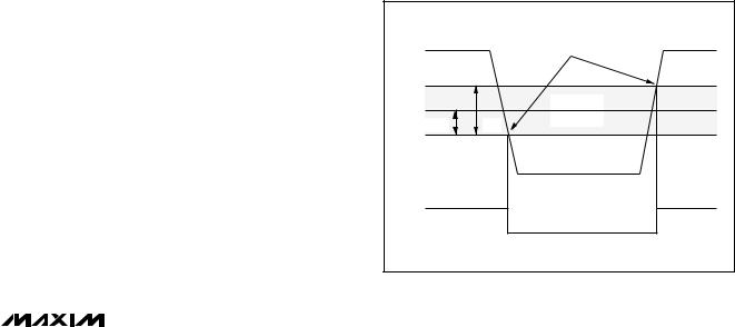
Ultra Low-Power, Low-Cost Comparators with 2% Reference
current falls. The reference will not function below about 2.2V, although the comparators will continue to operate with a total supply voltage as low as 1V. While the MAX934 has comparators that may be used at supply voltages below 2V, the MAX931, MAX932, and MAX933 may not be used with supply voltages significantly below 2.5V.
At low supply voltages, the comparators’ output drive is reduced and the propagation delay increases (see
Typical Operating Characteristics). The useful input voltage range extends from the negative supply to a little under 1V below the positive supply, which is slightly closer to the positive rail than the device operating from higher supply voltages. Test your prototype over the full temperature and supply-voltage range if operation below 2.5V is anticipated.
Comparator Output
With 100mV of overdrive, propagation delay is typically 3µs. The Typical Operating Characteristics show the propagation delay for various overdrive levels.
The MAX931 and MAX934 output swings from V+ to GND, so TTL compatibility is assured by using a +5V ±10% supply. The negative supply does not affect the output swing, and can range from 0V to -5V ±10%.
The MAX932 and MAX933 do not have a GND pin, and their outputs swing from V+ to V-. Connect V- to ground and V+ to a +5V supply to achieve TTL compatibility.
The MAX931-MAX934’s unique design achieves an output source current of more than 40mA and a sink current of over 5mA, while keeping quiescent currents in the microampere range. The output can source 100mA (at V+ = 5V) for short pulses, as long as the package's maximum power dissipation is not exceeded. The output stage does not generate crowbar switching currents during transitions, which minimizes feedback through the supplies and helps ensure stability without bypassing.
Voltage Reference
The internal bandgap voltage reference has an output of 1.182V above V-. Note that the REF voltage is referenced to V-, not to GND. Its accuracy is ±2% in the range 0°C to +70°C. The REF output is typically capable of sourcing 15µA and sinking 8µA. Do not bypass the REF output. For applications that require a 1% precision reference, see the MAX921-MAX924 data sheet.
Noise Considerations
Although the comparators have a very high gain, useful gain is limited by noise. This is shown in the Transfer Function graph (see Typical Operating Characteristics).
As the input voltage approaches the comparator's offset, the output begins to bounce back and forth; this peaks when VIN = VOS. (The lowpass filter shown on the graph averages out the bouncing, making the transfer function easy to observe.) Consequently, the comparator has an effective wideband peak-to-peak noise of around 0.3mV. The voltage reference has peak-to peak noise approaching 1mV. Thus, when a comparator is used with the reference, the combined peak-to-peak noise is about 1mV. This, of course, is much higher than the RMS noise of the individual components. Care should be taken in the layout to avoid capacitive coupling from any output to the reference pin. Crosstalk can significantly increase the actual noise of the reference.
__________Applications Information
Hysteresis
Hysteresis increases the comparators’ noise margin by increasing the upper threshold and decreasing the lower threshold (see Figure 2).
Hysteresis (MAX931/MAX932/MAX933)
To add hysteresis to the MAX931/MAX932/MAX933, connect resistor R1 between REF and HYST, and connect resistor R2 between HYST and V- (Figure 3). If no hysteresis is required, connect HYST to REF. When hysteresis is added, the upper threshold increases by the same amount that the lower threshold decreases. The hysteresis band (the difference between the upper and lower thresholds, VHB) is approximately equal to twice the voltage between REF and HYST. The HYST input can be adjusted to a maximum voltage of REF and to a minimum voltage of (REF - 50mV). The
IN+ |
|
THRESHOLDS |
|
|
|
||
IN- |
|
HYSTERESIS |
|
|
BAND |
||
VREF - VHYST |
VHB |
||
|
|||
OUT |
|
|
Figure 2. Threshold Hysteresis Band
MAX934-MAX931
_______________________________________________________________________________________ 9

MAX931-MAX934
Ultra Low-Power, Low-Cost Comparators with 2% Reference
maximum difference between REF and HYST (50mV) will therefore produce a 100mV max hysteresis band. Use the following equations to determine R1 and R2:
R1 |
= |
|
VHB |
|
|
|
(2 |
´ IREF ) |
|
|
|||
|
|
|
|
|||
|
|
æ |
|
|
V |
ö |
|
|
ç1.182 – |
|
HB |
÷ |
|
|
|
|
|
|||
R2 |
= |
è |
|
|
2 |
ø |
|
|
|
|
|
||
IREF
Where IREF (the current sourced by the reference) should not exceed the REF source capability, and should be significantly larger than the HYST input current. IREF values between 0.1µA and 4µA are usually appropriate. If 2.4MΩ is chosen for
R2 (IREF = 0.5µA), the equation for R1 and VHB can be approximated as:
R1 (kW) = VHB (mV)
When hysteresis is obtained in this manner for the MAX932/MAX933, the same hysteresis applies to both comparators.
Hysteresis (MAX934)
Hysteresis can be set with two resistors using positive feedback, as shown in Figure 4. This circuit generally draws more current than the circuits using the HYST pin on the MAX931/MAX932/MAX933, and the high feedback impedance slows hysteresis. The design procedure is as follows:
1.Choose R3. The leakage current of IN+ is under 1nA (up to +85°C), so the current through R3 can be around 100nA and still maintain good accuracy.
The current through R3 at the trip point is VREF/R3, or 100nA for R3 = 11.8MΩ . 10MΩ is a good practical value.
2.Choose the hysteresis voltage (VHB), the voltage between the upper and lower thresholds. In this example, choose VHB = 50mV.
3.Calculate R1.
R1 = R3 ´ VHB V +
= 10M ´ 0.05 5
=100kW
4.Choose the threshold voltage for VIN rising (VTHR). In this example, choose VTHR = 3V.
5.Calculate R2.
R2 = |
|
|
|
1 |
|
|
|
|
|
|
|
|
|
|
|
|
|
|
|
éæ |
VTHR |
|
ö |
|
1 |
|
|
|
|
1 |
ù |
|
|
|
|
||||
|
|
|
|
|
|
|
|
|
|
||||||||||
|
êç |
|
|
÷ |
- |
R1 |
- |
R3 |
ú |
|
|
|
|
||||||
|
êè |
(VREF × R1) ø |
|
|
|
ú |
|
|
|
|
|||||||||
|
ë |
|
|
|
|
|
|
|
|
|
|
|
û |
|
|
|
|
||
= |
|
|
|
|
1 |
|
|
|
|
|
|
|
|
|
|
|
|
||
éæ |
3 |
|
|
|
ö |
- |
|
|
1 |
|
- |
1 |
ù |
||||||
|
êç |
|
|
|
|
|
÷ |
|
|
|
|
|
|
ú |
|||||
|
(1.182 ´ |
|
|
|
|
|
|
|
|
|
|
||||||||
|
êè |
100k)ø |
|
|
100k |
10M ú |
|||||||||||||
|
ë |
|
|
|
|
|
|
|
|
|
|
|
|
|
|
|
|
û |
|
= 65.44kW
A 1% preferred value is 64.9kΩ .
6. Verify the threshold voltages with these formulas:
V |
rising : |
|
|
|
|
|
|
|
|
|
||
IN |
|
|
|
|
|
|
|
|
|
|
|
|
V |
|
= |
V |
´ R1 ´ |
æ 1 |
|
+ |
1 |
+ |
1 ö |
||
|
ç |
|
|
|
|
÷ |
||||||
THR |
|
REF |
|
|
|
|
R2 |
|||||
|
|
|
|
|
è R1 |
|
R3 ø |
|||||
VIN falling :
VTHF = VTHR - (R1 ´ V +)
R3
|
|
|
2.5V TO 11V |
|
IREF |
|
|
7 |
|
6 |
REF |
V+ |
||
|
||||
|
|
|
||
R1 |
|
|
MAX931 |
|
|
|
|
MAX932 |
|
|
5 |
|
MAX933 |
|
|
HYST |
|||
|
|
|||
R2 |
|
|
V- |
|
|
|
|
2 |
|
|
V+ |
|
R3 |
R1 |
|
VIN |
|
|
OUT |
R2 |
MAX934 VV+- |
|
GND |
|
VREF |
Figure 3. Programming the HYST Pin |
Figure 4. External Hysteresis |
10 ______________________________________________________________________________________