


PIC18F2455/2550/4455/4550
1.2Other Special Features
•Memory Endurance: The Enhanced Flash cells for both program memory and data EEPROM are rated to last for many thousands of erase/write cycles – up to 100,000 for program memory and 1,000,000 for EEPROM. Data retention without refresh is conservatively estimated to be greater than 40 years.
•Self-Programmability: These devices can write to their own program memory spaces under internal software control. By using a bootloader routine, located in the protected Boot Block at the top of program memory, it becomes possible to create an application that can update itself in the field.
•Extended Instruction Set: The PIC18F2455/2550/4455/4550 family introduces an optional extension to the PIC18 instruction set, which adds 8 new instructions and an Indexed Literal Offset Addressing mode. This extension, enabled as a device configuration option, has been specifically designed to optimize re-entrant application code originally developed in high-level languages such as C.
•Enhanced CCP Module: In PWM mode, this module provides 1, 2 or 4 modulated outputs for controlling half-bridge and full-bridge drivers. Other features include auto-shutdown for disabling PWM outputs on interrupt or other select conditions and auto-restart to reactivate outputs once the condition has cleared.
•Enhanced Addressable USART: This serial communication module is capable of standard RS-232 operation and provides support for the LIN bus protocol. Other enhancements include Automatic Baud Rate Detection and a 16-bit Baud Rate Generator for improved resolution. When the microcontroller is using the internal oscillator block, the EUSART provides stable operation for applications that talk to the outside world without using an external crystal (or its accompanying power requirement).
•10-Bit A/D Converter: This module incorporates programmable acquisition time, allowing for a channel to be selected and a conversion to be initiated, without waiting for a sampling period and thus, reducing code overhead.
•Dedicated ICD/ICSP Port: These devices introduce the use of debugger and programming pins that are not multiplexed with other microcontroller features. Offered as an option in select packages, this feature allows users to develop I/O intensive applications while retaining the ability to program and debug in the circuit.
1.3Details on Individual Family Members
Devices in the PIC18F2455/2550/4455/4550 family are available in 28-pin and 40/44-pin packages. Block diagrams for the two groups are shown in Figure 1-1 and Figure 1-2.
The devices are differentiated from each other in six ways:
1.Flash program memory (24 Kbytes for
PIC18FX455 |
devices, |
32 Kbytes |
for |
PIC18FX550). |
|
|
|
2.A/D channels (10 for 28-pin devices, 13 for 40/44-pin devices).
3.I/O ports (3 bidirectional ports and 1 input only port on 28-pin devices, 5 bidirectional ports on 40/44-pin devices).
4.CCP and Enhanced CCP implementation (28-pin devices have two standard CCP modules, 40/44-pin devices have one standard CCP module and one ECCP module).
5.Streaming Parallel Port (present only on 40/44-pin devices).
All other features for devices in this family are identical. These are summarized in Table 1-1.
The pinouts for all devices are listed in Table 1-2 and Table 1-3.
Like all Microchip PIC18 devices, members of the PIC18F2455/2550/4455/4550 family are available as both standard and low-voltage devices. Standard devices with Enhanced Flash memory, designated with an “F” in the part number (such as PIC18F2550), accommodate an operating VDD range of 4.2V to 5.5V. Low-voltage parts, designated by “LF” (such as PIC18LF2550), function over an extended VDD range of 2.0V to 5.5V.
DS39632D-page 8 |
Preliminary |
♥ 2007 Microchip Technology Inc. |
PIC18F2455/2550/4455/4550
TABLE 1-1: |
DEVICE FEATURES |
|
|
|
|
|
|
|
|
|
|||
Features |
|
PIC18F2455 |
|
PIC18F2550 |
|
PIC18F4455 |
|
PIC18F4550 |
|||||
|
|
|
|
|
|
|
|
|
|||||
|
|
|
|
|
|
|
|
|
|||||
Operating Frequency |
|
DC – 48 MHz |
|
DC – 48 MHz |
|
DC – 48 MHz |
|
DC – 48 MHz |
|||||
|
|
|
|
|
|||||||||
Program Memory (Bytes) |
24576 |
32768 |
24576 |
32768 |
|||||||||
|
|
|
|
|
|||||||||
Program Memory (Instructions) |
12288 |
16384 |
12288 |
16384 |
|||||||||
|
|
|
|
|
|||||||||
Data Memory (Bytes) |
2048 |
2048 |
2048 |
2048 |
|||||||||
|
|
|
|
|
|||||||||
Data EEPROM Memory (Bytes) |
256 |
256 |
256 |
256 |
|||||||||
|
|
|
|
|
|
||||||||
Interrupt Sources |
|
19 |
19 |
20 |
20 |
||||||||
|
|
|
|
|
|
||||||||
I/O Ports |
|
Ports A, B, C, (E) |
Ports A, B, C, (E) |
Ports A, B, C, D, E |
Ports A, B, C, D, E |
||||||||
|
|
|
|
|
|
||||||||
Timers |
|
4 |
4 |
4 |
4 |
||||||||
|
|
|
|
|
|||||||||
Capture/Compare/PWM Modules |
2 |
2 |
1 |
1 |
|||||||||
|
|
|
|
|
|||||||||
Enhanced Capture/ |
0 |
0 |
1 |
1 |
|||||||||
Compare/PWM Modules |
|
|
|
|
|
|
|
|
|
|
|
|
|
|
|
|
|
|
|
|
|
|
|||||
Serial Communications |
|
MSSP, |
|
MSSP, |
|
MSSP, |
|
MSSP, |
|||||
|
|
Enhanced USART |
Enhanced USART |
Enhanced USART |
Enhanced USART |
||||||||
|
|
|
|
|
|||||||||
Universal Serial Bus (USB) |
1 |
1 |
1 |
1 |
|||||||||
Module |
|
|
|
|
|
|
|
|
|
|
|
|
|
|
|
|
|
|
|
|
|
|
|
|
|
|
|
Streaming Parallel Port (SPP) |
|
|
No |
|
|
No |
|
|
Yes |
|
|
Yes |
|
|
|
|
|
|
|||||||||
10-Bit Analog-to-Digital Module |
10 Input Channels |
10 Input Channels |
13 Input Channels |
13 Input Channels |
|||||||||
|
|
|
|
|
|
||||||||
Comparators |
|
2 |
2 |
2 |
2 |
||||||||
|
|
|
|
|
|
|
|
|
|||||
Resets (and Delays) |
|
POR, BOR, |
|
POR, BOR, |
|
POR, BOR, |
|
POR, BOR, |
|||||
|
|
RESET Instruction, |
RESET Instruction, |
RESET Instruction, |
RESET Instruction, |
||||||||
|
|
|
Stack Full, |
|
Stack Full, |
|
Stack Full, |
|
Stack Full, |
||||
|
|
|
Stack Underflow |
|
Stack Underflow |
|
Stack Underflow |
|
Stack Underflow |
||||
|
|
|
(PWRT, OST), |
|
(PWRT, OST), |
|
(PWRT, OST), |
|
(PWRT, OST), |
||||
|
|
|
MCLR |
(optional), |
|
MCLR |
(optional), |
|
MCLR |
(optional), |
|
MCLR |
(optional), |
|
|
|
WDT |
|
WDT |
|
WDT |
|
WDT |
||||
|
|
|
|
|
|
|
|
|
|
|
|
|
|
Programmable Low-Voltage |
|
|
Yes |
|
|
Yes |
|
|
Yes |
|
|
Yes |
|
Detect |
|
|
|
|
|
|
|
|
|
|
|
|
|
|
|
|
|
|
|
|
|
|
|
|
|
|
|
Programmable Brown-out Reset |
|
|
Yes |
|
|
Yes |
|
|
Yes |
|
|
Yes |
|
|
|
|
|
|
|
|
|
|
|
||||
Instruction Set |
|
|
75 Instructions; |
|
75 Instructions; |
|
75 Instructions; |
|
75 Instructions; |
||||
|
|
83 with Extended |
83 with Extended |
83 with Extended |
83 with Extended |
||||||||
|
|
|
Instruction Set |
|
Instruction Set |
|
Instruction Set |
|
Instruction Set |
||||
|
|
|
enabled |
|
enabled |
|
enabled |
|
enabled |
||||
|
|
|
|
|
|
|
|
|
|
||||
Packages |
|
|
28-pin PDIP |
|
28-pin PDIP |
|
40-pin PDIP |
|
40-pin PDIP |
||||
|
|
|
28-pin SOIC |
|
28-pin SOIC |
|
44-pin QFN |
|
44-pin QFN |
||||
|
|
|
|
|
|
|
|
|
44-pin TQFP |
|
44-pin TQFP |
||
|
|
|
|
|
|
|
|
|
|
|
|
|
|
♥ 2007 Microchip Technology Inc.
Preliminary
DS39632D-page 9
PIC18F2455/2550/4455/4550 |
|
|||||
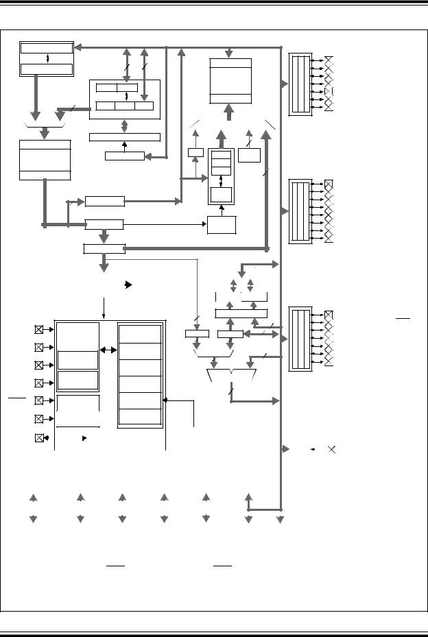
FIGURE 1-1: |
PIC18F2455/2550 (28-PIN) BLOCK DIAGRAM |
|
||||
Table Pointer<21> |
|
Data Bus<8> |
|
|
|
PORTA |
|
|
|
|
|
||
|
8 |
8 |
Data Latch |
|
RA0/AN0 |
|
inc/dec logic |
|
RA1/AN1 |
||||
|
|
|
||||
|
|
|
Data Memory |
|
RA2/AN2/VREF-/CVREF |
|
21 |
PCLATU PCLATH |
|
(2 Kbytes) |
|
RA3/AN3/VREF+ |
|
|
|
|
|
RA4/T0CKI/C1OUT/RCV |
||
|
|
|
|
|
||
|
|
|
|
|
|
|
20 |
PCU PCH |
PCL |
Address Latch |
|
RA5/AN4/SS/HLVDIN/C2OUT |
|
|
|
|
|
OSC2/CLKO/RA6 |
||
|
Program Counter |
|
12 |
|
|
|
|
|
|
Data Address<12> |
|
||
|
31 Level Stack |
|
|
|
|
|
Address Latch |
|
4 |
12 |
|
4 |
|
Program Memory |
STKPTR |
BSR |
FSR0 |
Access |
|
|
|
Bank |
|
||||
(24/32 Kbytes) |
|
|
FSR1 |
|
||
|
|
|
|
|
||
Data Latch |
|
|
FSR2 |
|
12 |
PORTB |
|
|
|
|
|||
|
|
|
inc/dec |
|
|
RB0/AN12/INT0/FLT0/SDI/SDA |
8 |
|
|
|
|
RB1/AN10/INT1/SCK/SCL |
|
Table Latch |
|
logic |
|
|
RB2/AN8/INT2/VMO |
|
|
|
|
|
|
||
|
|
|
|
|
|
RB3/AN9/CCP2(3)/VPO |
|
|
|
Address |
|
|
RB4/AN11/KBI0 |
|
ROM Latch |
|
|
|
RB5/KBI1/PGM |
|
Instruction Bus <16> |
|
|
Decode |
|
|
RB6/KBI2/PGC |
|
|
|
|
|
|
RB7/KBI3/PGD |
|
IR |
|
|
|
|
|
8 |
Instruction |
|
State Machine |
|
|
|
|
||
|
|
|
||||||
Decode & |
|
|
Control Signals |
|
|
|
||
Control |
|
|
|
|
||||
|
|
PRODH PRODL |
||||||
|
|
|
|
|||||
|
|
|
|
|||||
|
|
|
|
|
|
PORTC |
|
|
|
|
3 |
8 x 8 Multiply |
|
RC0/T1OSO/T13CKI |
|
|
|
|
|
8 |
RC1/T1OSI/CCP2 |
(3) |
|
OSC1(2) |
Internal |
|
|
|
|
/UOE |
|
Power-up |
BITOP |
W |
|
RC2/CCP1 |
|
||
|
Oscillator |
Timer |
8 |
RC4/D-/VM |
|
||
|
Block |
8 |
8 |
|
|||
OSC2(2) |
Oscillator |
|
RC5/D+/VP |
|
|||
|
|
|
|
|
|||
|
INTRC |
Start-up Timer |
|
8 |
|
RC6/TX/CK |
|
T1OSI |
Oscillator |
Power-on |
|
8 |
RC7/RX/DT/SDO |
|
|
|
Reset |
|
|
|
|
|
|
|
8 MHz |
|
ALU<8> |
|
|
|
|
|
Watchdog |
|
|
|
|
||
T1OSO |
Oscillator |
|
|
|
|
|
|
Timer |
|
|
|
|
|
||
|
|
|
8 |
|
|
|
|
|
|
Brown-out |
|
|
|
|
|
MCLR(1) |
Single-Supply |
|
|
|
|
|
|
Reset |
|
|
|
|
|
||
|
Programming |
|
|
|
|
|
|
|
Fail-Safe |
|
|
|
|
|
|
VDD,VSS |
In-Circuit |
|
|
|
|
|
|
Debugger |
Clock Monitor |
|
|
|
|
|
|
|
|
|
|
|
|
|
|
|
|
|
|
|
|
|
|
|
|
|
|
|
|
|
|
|
|
|
|
|
|
|
|
|
Band Gap |
|
|
|
|
|
|
|
|
|
|
PORTE |
|||||||||||||
VUSB |
|
|
|
|
|
|
|
USB Voltage |
|
|
|
|
|
|
|
|
|
|
|
|
|
|
|
|
|
|
|
|
|
|
|
|
|
|
|||||||||||||||
|
|
|
|
|
|
|
|
|
|
|
|
|
|
|
|
|
|
|
|
|
|
|
|
||||||||||||||||||||||||||
|
|
|
|
|
|
|
Regulator |
|
|
|
|
|
|
|
Reference |
|
|
|
|
|
|
|
|
|
|
|
|
|
|
|
|
|
|
|
PP/RE3(1) |
||||||||||||||
|
|
|
|
|
|
|
|
|
|
|
|
|
|
|
|
|
|
|
|
|
|
|
|
|
|
|
|
|
|
|
|
|
|
|
|
|
|||||||||||||
|
|
|
|
|
|
|
|
|
|
|
|
|
|
|
|
|
|
|
|
|
|
|
|
|
|
|
|
|
|
|
|
|
|
|
|
|
|
|
|
|
|
|
|
|
|
|
|
MCLR/V |
|
|
|
|
|
|
|
|
|
|
|
|
|
|
|
|
|
|
|
|
|
|
|
|
|
|
|
|
|
|
|
|
|
|
|
|
|
|
|
|
|
|
|
|
|
|
|
|
|
|
|
|
|
|
|
|
|
|
|
|
|
|
|
|
|
|
|
|
|
|
|
|
|
|
|
|
|
|
|
|
|
|
|
|
|
|
|
|
|
|
|
|
|
|
|
|
|
|
|
|
|
|
|
|
|
|
|
|
|
|
|
|
|
|
|
|
|
|
|
|
|
|
|
|
|
|
|
|
|
|
|
|
|
|
|
|
|
|
|
|
|
|
|
|
|
|
|
|
|
|
|
|
|
|
|
|
|
|
|
|
|
|
|
|
|
|
|
|
|
|
|
|
|
|
|
|
|
|
|
|
|
|
|
|
|
|
|
|
|
|
|
|
|
|
|
|
|
|
|
|
|
|
BOR |
|
|
Data |
|
Timer0 |
|
Timer1 |
|
Timer2 |
|
Timer3 |
|
|
|
|
|
|
|
|
|
|
|
|
|
|
|||||||||||||||||||||||
|
HLVD |
|
|
EEPROM |
|
|
|
|
|
|
|
||||||||||||||||||||||||||||||||||||||
|
|
|
|
|
|
|
|
|
|
|
|
|
|
|
|
|
|
|
|
|
|
|
|
|
|
|
|
|
|
|
|
|
|
|
|
|
|
|
|
||||||||||
|
|
|
|
|
|
|
|
|
|
|
|
|
|
|
|
|
|
|
|
|
|
|
|
|
|
|
|
|
|
|
|
|
|
|
|
|
|
|
|
|
|
|
|
|
|
|
|
|
|
|
|
|
|
|
|
|
|
|
|
|
|
|
|
|
|
|
|
|
|
|
|
|
|
|
|
|
|
|
|
|
|
|
|
|
|
|
|
|
|
|
|
|
|
|
|
|
|
|
|
|
|
|
|
|
|
|
|
|
|
|
|
|
|
|
|
|
|
|
|
|
|
|
|
|
|
|
|
|
|
|
|
|
|
|
|
|
|
|
|
|
|
|
|
|
|
|
|
|
|
|
|
|
|
|
|
|
|
|
|
|
|
|
|
|
|
|
|
|
|
|
|
|
|
|
|
|
|
|
|
|
|
|
|
|
|
|
|
|
|
|
|
|
|
|
|
|
|
|
|
Comparator |
|
CCP1 |
|
CCP2 |
|
MSSP |
|
EUSART |
|
ADC |
|
USB |
|
|
|
|
|
10-Bit |
|
||||||
|
|
|
|
|
|
|
|
|
|
|
|
|
|
|
|
|
|
|
|
|
|
|
|
|
|
Note 1: RE3 is multiplexed with MCLR and is only available when the MCLR Resets are disabled.
2:OSC1/CLKI and OSC2/CLKO are only available in select oscillator modes and when these pins are not being used as digital I/O. Refer to Section 2.0 “Oscillator Configurations” for additional information.
3:RB3 is the alternate pin for CCP2 multiplexing.
DS39632D-page 10 |
Preliminary |
♥ 2007 Microchip Technology Inc. |

PIC18F2455/2550/4455/4550
FIGURE 1-2: PIC18F4455/4550 (40/44-PIN) BLOCK DIAGRAM
|
|
|
|
|
|
|
|
|
|
|
|
|
|
|
|
|
|
|
|
|
|
|
|
|
Data Bus<8> |
|
|
|
|
|
|
|
|
|
|
|
|
|
|
|
|
|||||||||
|
Table Pointer<21> |
|
|
|
|
|
|
|
|
|
|
|
|
|
|
|
|
|
|
|
|
|
|
|
|
|
|
|
|
|
|
|
|
|
|
|
|
|
|
|||||||||||
|
|
|
|
|
|
|
|
|
|
|
|
|
|
|
|
|
|
|
|
|
|
|
|
|
|
|
|
|
|
|
|
|
|
|
|
|
|
|
|
|
|
|
|
|
|
|
|
|
|
|
|
|
|
|
|
|
|
|
|
|
|
|
|
|
|
|
|
|
|
|
|
8 |
|
|
8 |
|
|
|
|
|
|
|
|
|
|
Data Latch |
|
|
|
|
|
||||||||||
|
inc/dec logic |
|
|
|
|
|
|
|
|
|
|
|
|
|
|
|
|
|
|
|
Data Memory |
|
|
|
|
|
||||||||||||||||||||||||
|
|
|
|
|
|
|
|
|
|
|
|
|
|
|
|
|
|
|
|
|
|
|
|
|
|
|
|
|
|
|
|
|
|
|
|
|
|
|
|
|
|
|||||||||
|
|
|
|
|
|
|
|
|
|
|
|
|
|
|
|
|
|
|
|
|
|
|
|
|
|
|
|
|
|
|
|
|
|
|
|
|
|
|
|
|
|
|||||||||
|
|
|
|
|
|
|
|
|
|
|
|
|
|
|
|
|
|
|
|
|
|
|
|
|
|
|
|
|
|
|
|
|
|
|
|
|
(2 Kbytes) |
|
|
|
|
|
||||||||
|
|
|
|
21 |
|
|
|
|
|
|
|
|
|
PCLATU |
PCLATH |
|
|
|
|
|
|
|
|
|
|
|
|
|
|
|
|
|
|
|||||||||||||||||
|
|
|
|
|
|
|
|
|
|
|
|
|
|
|
|
|
|
|
|
|
|
|
|
|
|
|
|
|
|
|
|
|
|
|
|
|
|
|||||||||||||
|
|
|
|
|
|
|
|
|
|
|
|
|
|
|
|
|
|
|
|
|
|
|
|
|
|
|
|
|
|
|
|
|
|
|
|
|
|
|
|
|
|
|
|
|
|
|
|
|
|
|
|
|
|
20 |
|
|
|
|
|
|
|
|
|
|
|
|
|
|
|
|
|
|
|
|
|
|
|
Address Latch |
|
|
|
|
|
||||||||||||||||||
|
|
|
|
|
|
|
|
|
|
|
|
|
|
|
|
|
|
|
|
|
|
|
|
|
|
|
|
|
|
|||||||||||||||||||||
|
|
|
|
|
|
|
|
|
|
|
|
|
|
|
|
|
PCU |
PCH |
|
PCL |
|
|
|
|
|
|
|
|
|
|
|
|
|
|
|
|
|
|
|
|
|
|
|
|||||||
|
|
|
|
|
|
|
|
|
|
|
|
|
|
|
|
|
|
|
|
|
|
|
|
|
|
|
|
|
|
|
|
|
||||||||||||||||||
|
|
|
|
|
|
|
|
|
|
|
|
|
|
|
|
|
Program Counter |
|
|
|
|
|
|
|
|
|
|
|
|
|
|
|
|
12 |
|
|
|
|
|
|
||||||||||
|
|
|
|
|
|
|
|
|
|
|
|
|
|
|
|
|
|
|
|
|
|
|
|
|
|
|
|
|
|
|
|
|
|
|
Data Address<12> |
|
|
|||||||||||||
|
|
|
|
|
|
|
|
|
|
|
|
|
|
|
|
|
|
|
|
|
|
|
|
|
|
|
|
|
|
|
|
|
|
|
|
|
||||||||||||||
|
|
|
|
|
|
|
|
|
|
|
|
|
|
|
|
|
31 Level Stack |
|
|
|
|
|
|
|
|
|
|
|
|
|
|
|
|
|
|
|
|
|
|
|
||||||||||
|
|
|
|
|
|
|
|
|
|
|
|
|
|
|
|
|
|
|
|
|
|
|
|
|
|
|
|
|
|
|
|
|
4 |
|
|
|
12 |
|
|
|
4 |
|
|
|
|
|||||
|
Address Latch |
|
|
|
|
|
|
|
|
|
|
|
|
|
|
|
|
|
|
|
|
|
|
|||||||||||||||||||||||||||
|
|
|
|
|
|
|
|
|
|
|
|
|
|
|
|
|
|
|
|
|
|
|
|
|
|
|
|
|
|
|
|
|
|
|
|
|
|
|
|
|
|
|
|
|
|
|
|
|
|
|
|
|
|
|
|
|
|
|
|
|
|
|
|
|
|
|
|
|
|
|
|
|
|
|
|
|
|
|
|
|
|
|
BSR |
|
|
|
|
|
|
|
|
|
Access |
|
|
|
|
||||
Program Memory |
|
STKPTR |
|
|
|
|
|
|
|
|
|
|
|
|
|
FSR0 |
|
Bank |
|
|
|
|
||||||||||||||||||||||||||||
|
(24/32 Kbytes) |
|
|
|
|
|
|
|
|
|
|
|
|
|
|
|
|
|
|
|
|
FSR1 |
|
|
|
|
|
|
||||||||||||||||||||||
|
|
|
|
|
|
|
|
|
|
|
|
|
|
|
|
|
|
|
|
|
|
|
|
|
|
|
||||||||||||||||||||||||
|
|
|
|
|
|
|
|
|
|
|
|
|
|
|
|
|
|
|
|
|
|
|
|
|
|
|
|
|
||||||||||||||||||||||
|
Data Latch |
|
|
|
|
|
|
|
|
|
|
|
|
|
|
|
|
|
|
|
|
|
FSR2 |
|
12 |
|
|
|
||||||||||||||||||||||
|
|
|
|
|
|
|
|
|
|
|
|
|
|
|
|
|
|
|
|
|
|
|
|
|
|
|
|
|
|
|
||||||||||||||||||||
8 |
|
inc/dec |
|
Table Latch |
logic |
||
|
|
||
|
ROM Latch |
Address |
|
Instruction Bus <16> |
Decode |
||
|
|||
|
|
||
|
IR |
|
8 |
|
Instruction |
State Machine |
|
|
|
|
Decode & |
Control Signals |
|
|
|
|
Control |
|
|
|
|
|
|
|
PRODH PRODL |
||
|
|
|
|
||
VDD, VSS |
|
|
3 |
8 x 8 Multiply |
|
Internal |
|
|
8 |
||
|
Power-up |
|
|
|
|
OSC1(2) |
Oscillator |
BITOP |
W |
|
|
Timer |
|
||||
|
Block |
8 |
8 |
8 |
|
OSC2(2) |
|
||||
INTRC |
Oscillator |
|
|
|
|
|
Start-up Timer |
|
|
|
|
T1OSI |
Oscillator |
|
8 |
8 |
|
|
|
||||
|
Power-on |
|
|||
T1OSO |
8 MHz |
|
|
|
|
Reset |
|
ALU<8> |
|
||
Oscillator |
|
|
|||
|
|
|
|
|
|
|
|
Watchdog |
|
8 |
|
ICPGC(3) |
Single-Supply |
Timer |
|
|
|
|
|
|
|||
ICPGD(3) |
Programming |
Brown-out |
|
|
|
In-Circuit |
Reset |
|
|
|
|
|
|
|
|
||
ICPORTS(3) |
|
|
|
|
|
Debugger |
Fail-Safe |
|
|
|
|
ICRST(3) |
|
Clock Monitor |
Band Gap |
|
|
|
|
Reference |
|
|
|
|
|
|
|
|
|
MCLR(1) |
USB Voltage |
|
|
|
|
|
Regulator |
|
|
|
|
VUSB |
|
|
|
|
|
BOR |
|
Data |
|
Timer0 |
|
Timer1 |
|
Timer2 |
|
Timer3 |
|
|
||||||||||||||||||
HLVD |
|
EEPROM |
|
|
|
|
|
|
||||||||||||||||||||||
|
|
|
|
|
|
|
|
|
|
|
|
|
|
|
|
|
|
|
|
|
|
|
||||||||
|
|
|
|
|
|
|
|
|
|
|
|
|
|
|
|
|
|
|
|
|
|
|
|
|
|
|
|
|
|
|
|
|
|
|
|
|
|
|
|
|
|
|
|
|
|
|
|
|
|
|
|
|
|
|
|
|
|
|
|
|
|
|
|
|
|
|
|
|
|
|
|
|
|
|
|
|
|
|
|
|
|
|
|
|
|
|
|
|
|
|
|
|
|
|
|
|
|
|
|
|
|
|
|
|
|
|
|
|
|
|
|
|
|
|
|
|
|
|
|
|
|
|
|
PORTA

 RA0/AN0
RA1/AN1


 RA2/AN2/VREF-/CVREF
RA3/AN3/VREF+

 RA4/T0CKI/C1OUT/RCV
RA5/AN4/SS/HLVDIN/C2OUT

 OSC2/CLKO/RA6
PORTB |
RB0/AN12/INT0/FLT0/SDI/SDA |
RB1/AN10/INT1/SCK/SCL |
RB2/AN8/INT2/VMO |
RB3/AN9/CCP2(4)/VPO |
RB4/AN11/KBI0/CSSPP |
RB5/KBI1/PGM |
RB6/KBI2/PGC |
RB7/KBI3/PGD |
PORTC |
RC0/T1OSO/T13CKI |
RC1/T1OSI/CCP2(4)/UOE |
RC2/CCP1/P1A |
RC4/D-/VM |
RC5/D+/VP |
RC6/TX/CK |
RC7/RX/DT/SDO |
PORTD |

 RD0/SPP0:RD4/SPP4
RD5/SPP5/P1B

 RD6/SPP6/P1C
RD7/SPP7/P1D
PORTE


 RE0/AN5/CK1SPP
RE1/AN6/CK2SPP

 RE2/AN7/OESPP
MCLR/VPP/RE3(1)
Comparator |
|
ECCP1 |
|
CCP2 |
|
MSSP |
|
EUSART |
|
ADC |
|
USB |
|
|
|
|
|
10-Bit |
|
||||||
|
|
|
|
|
|
|
|
|
|
|
|
|
|
|
|
|
|
|
|
|
|
|
|
|
|
Note 1: RE3 is multiplexed with MCLR and is only available when the MCLR Resets are disabled.
2:OSC1/CLKI and OSC2/CLKO are only available in select oscillator modes and when these pins are not being used as digital I/O. Refer to Section 2.0 “Oscillator Configurations” for additional information.
3:These pins are only available on 44-pin TQFP packages under certain conditions. Refer to Section 25.9 “Special ICPORT Features (Designated Packages Only)” for additional information.
4:RB3 is the alternate pin for CCP2 multiplexing.
♥ 2007 Microchip Technology Inc.
Preliminary
DS39632D-page 11

PIC18F2455/2550/4455/4550
TABLE 1-2: |
PIC18F2455/2550 PINOUT I/O DESCRIPTIONS |
|||||||
|
|
|
|
Pin |
|
|
|
|
|
|
Pin Name |
Number |
Pin |
Buffer |
|
Description |
|
|
|
|
|
|||||
|
|
PDIP, |
Type |
Type |
|
|||
|
|
|
|
|
|
|||
|
|
|
|
|
|
|
|
|
|
|
|
|
SOIC |
|
|
|
|
|
|
|
|
|
|
|||
|
|
|
|
|
|
|
|
|
|
|
/VPP/RE3 |
1 |
|
|
Master Clear (input) or programming voltage (input). |
||
|
MCLR |
|
|
|||||
|
MCLR |
|
|
I |
ST |
Master Clear (Reset) input. This pin is an active-low |
||
|
|
|
|
|
|
|
Reset to the device. |
|
|
VPP |
|
|
P |
|
Programming voltage input. |
||
|
RE3 |
|
|
I |
ST |
Digital input. |
||
|
|
|
|
|
|
|
||
|
OSC1/CLKI |
|
9 |
|
|
Oscillator crystal or external clock input. |
||
|
OSC1 |
|
|
I |
Analog |
Oscillator crystal input or external clock source input. |
||
|
CLKI |
|
|
I |
Analog |
External clock source input. Always associated with pin |
||
|
|
|
|
|
|
|
function OSC1. (See OSC2/CLKO pin.) |
|
|
|
|
|
|
|
|||
|
OSC2/CLKO/RA6 |
10 |
|
|
Oscillator crystal or clock output. |
|||
|
OSC2 |
|
|
O |
— |
Oscillator crystal output. Connects to crystal or resonator in |
||
|
|
|
|
|
|
|
Crystal Oscillator mode. |
|
|
CLKO |
|
|
O |
— |
In select modes, OSC2 pin outputs CLKO which has 1/4 the |
||
|
|
|
|
|
|
|
frequency of OSC1 and denotes the instruction cycle rate. |
|
|
RA6 |
|
|
I/O |
TTL |
General purpose I/O pin. |
||
|
|
|
|
|
|
|||
|
Legend: TTL = TTL compatible input |
|
CMOS = CMOS compatible input or output |
|||||
|
|
ST |
= Schmitt Trigger input with CMOS levels I |
= Input |
||||
|
|
O |
= Output |
|
|
|
P |
= Power |
Note 1: Alternate assignment for CCP2 when CCP2MX Configuration bit is cleared.
2:Default assignment for CCP2 when CCP2MX Configuration bit is set.
DS39632D-page 12 |
Preliminary |
♥ 2007 Microchip Technology Inc. |

|
|
|
|
|
|
PIC18F2455/2550/4455/4550 |
||
|
|
|
|
|
|
|
|
|
TABLE 1-2: |
PIC18F2455/2550 PINOUT I/O DESCRIPTIONS (CONTINUED) |
|||||||
|
|
|
|
Pin |
|
|
|
|
Pin Name |
Number |
Pin |
Buffer |
|
Description |
|||
|
|
|||||||
PDIP, |
Type |
Type |
|
|||||
|
|
|
|
|
|
|||
|
|
|
|
|
|
|
|
|
|
|
|
|
SOIC |
|
|
|
|
|
|
|
|
|
|
|
|
|
|
|
|
|
|
|
|
|
|
|
|
|
|
|
|
|
PORTA is a bidirectional I/O port. |
|
RA0/AN0 |
|
2 |
|
|
|
|
||
RA0 |
|
|
I/O |
TTL |
Digital I/O. |
|
||
AN0 |
|
|
I |
Analog |
Analog input 0. |
|||
RA1/AN1 |
|
3 |
|
|
|
|
||
RA1 |
|
|
I/O |
TTL |
Digital I/O. |
|
||
AN1 |
|
|
I |
Analog |
Analog input 1. |
|||
RA2/AN2/VREF-/CVREF |
4 |
|
|
|
|
|||
RA2 |
|
|
I/O |
TTL |
Digital I/O. |
|
||
AN2 |
|
|
I |
Analog |
Analog input 2. |
|||
VREF- |
|
|
I |
Analog |
A/D reference voltage (low) input. |
|||
CVREF |
|
|
O |
Analog |
Analog comparator reference output. |
|||
RA3/AN3/VREF+ |
5 |
|
|
|
|
|||
RA3 |
|
|
I/O |
TTL |
Digital I/O. |
|
||
AN3 |
|
|
I |
Analog |
Analog input 3. |
|||
VREF+ |
|
|
I |
Analog |
A/D reference voltage (high) input. |
|||
RA4/T0CKI/C1OUT/RCV |
6 |
|
|
|
|
|||
RA4 |
|
|
I/O |
ST |
Digital I/O. |
|
||
T0CKI |
|
|
I |
ST |
Timer0 external clock input. |
|||
C1OUT |
|
|
O |
— |
Comparator 1 output. |
|||
RCV |
|
|
I |
TTL |
External USB transceiver RCV input. |
|||
|
|
|
|
7 |
|
|
|
|
RA5/AN4/SS/ |
|
|
|
|
|
|
||
HLVDIN/C2OUT |
|
|
|
|
|
|||
RA5 |
|
|
I/O |
TTL |
Digital I/O. |
|
||
AN4 |
|
|
I |
Analog |
Analog input 4. |
|||
SS |
|
|
I |
TTL |
SPI slave select input. |
|||
HLVDIN |
|
|
I |
Analog |
High/Low-Voltage Detect input. |
|||
C2OUT |
|
|
O |
— |
Comparator 2 output. |
|||
RA6 |
|
— |
— |
— |
See the OSC2/CLKO/RA6 pin. |
|||
|
|
|
|
|
||||
Legend: TTL = TTL compatible input |
|
CMOS = CMOS compatible input or output |
||||||
|
ST |
= Schmitt Trigger input with CMOS levels I |
= Input |
|||||
|
O |
= Output |
|
|
|
P |
= Power |
|
Note 1: Alternate assignment for CCP2 when CCP2MX Configuration bit is cleared.
2:Default assignment for CCP2 when CCP2MX Configuration bit is set.
♥ 2007 Microchip Technology Inc.
Preliminary
DS39632D-page 13

PIC18F2455/2550/4455/4550
TABLE 1-2: |
PIC18F2455/2550 PINOUT I/O DESCRIPTIONS (CONTINUED) |
|||||
|
|
Pin |
|
|
|
|
Pin Name |
Number |
Pin |
Buffer |
Description |
||
|
||||||
PDIP, |
Type |
Type |
||||
|
|
|
||||
|
|
|
|
|
||
|
|
SOIC |
|
|
|
|
|
|
|
|
|
|
|
|
|
|
|
|
|
|
|
|
|
|
|
PORTB is a bidirectional I/O port. PORTB can be software |
|
|
|
|
|
|
programmed for internal weak pull-ups on all inputs. |
|
RB0/AN12/INT0/FLT0/ |
21 |
|
|
|
||
SDI/SDA |
|
|
|
|
|
|
RB0 |
|
|
I/O |
TTL |
Digital I/O. |
|
AN12 |
|
|
I |
Analog |
Analog input 12. |
|
INT0 |
|
|
I |
ST |
External interrupt 0. |
|
FLT0 |
|
|
I |
ST |
PWM Fault input (CCP1 module). |
|
SDI |
|
|
I |
ST |
SPI data in. |
|
SDA |
|
|
I/O |
ST |
I2C™ data I/O. |
|
RB1/AN10/INT1/SCK/ |
22 |
|
|
|
||
SCL |
|
|
|
|
|
|
RB1 |
|
|
I/O |
TTL |
Digital I/O. |
|
AN10 |
|
|
I |
Analog |
Analog input 10. |
|
INT1 |
|
|
I |
ST |
External interrupt 1. |
|
SCK |
|
|
I/O |
ST |
Synchronous serial clock input/output for SPI mode. |
|
SCL |
|
|
I/O |
ST |
Synchronous serial clock input/output for I2C mode. |
|
RB2/AN8/INT2/VMO |
23 |
|
|
|
||
RB2 |
|
|
I/O |
TTL |
Digital I/O. |
|
AN8 |
|
|
I |
Analog |
Analog input 8. |
|
INT2 |
|
|
I |
ST |
External interrupt 2. |
|
VMO |
|
|
O |
— |
External USB transceiver VMO output. |
|
RB3/AN9/CCP2/VPO |
24 |
|
|
|
||
RB3 |
|
|
I/O |
TTL |
Digital I/O. |
|
AN9 |
|
|
I |
Analog |
Analog input 9. |
|
CCP2(1) |
|
|
I/O |
ST |
Capture 2 input/Compare 2 output/PWM 2 output. |
|
VPO |
|
|
O |
— |
External USB transceiver VPO output. |
|
RB4/AN11/KBI0 |
|
25 |
|
|
|
|
RB4 |
|
|
I/O |
TTL |
Digital I/O. |
|
AN11 |
|
|
I |
Analog |
Analog input 11. |
|
KBI0 |
|
|
I |
TTL |
Interrupt-on-change pin. |
|
RB5/KBI1/PGM |
|
26 |
|
|
|
|
RB5 |
|
|
I/O |
TTL |
Digital I/O. |
|
KBI1 |
|
|
I |
TTL |
Interrupt-on-change pin. |
|
PGM |
|
|
I/O |
ST |
Low-Voltage ICSP™ Programming enable pin. |
|
RB6/KBI2/PGC |
|
27 |
|
|
|
|
RB6 |
|
|
I/O |
TTL |
Digital I/O. |
|
KBI2 |
|
|
I |
TTL |
Interrupt-on-change pin. |
|
PGC |
|
|
I/O |
ST |
In-Circuit Debugger and ICSP programming clock pin. |
|
RB7/KBI3/PGD |
|
28 |
|
|
|
|
RB7 |
|
|
I/O |
TTL |
Digital I/O. |
|
KBI3 |
|
|
I |
TTL |
Interrupt-on-change pin. |
|
PGD |
|
|
I/O |
ST |
In-Circuit Debugger and ICSP programming data pin. |
|
|
|
|
|
|
|
|
Legend: TTL = TTL compatible input |
CMOS = CMOS compatible input or output |
||
ST |
= Schmitt Trigger input with CMOS levels |
I |
= Input |
O |
= Output |
P |
= Power |
Note 1: Alternate assignment for CCP2 when CCP2MX Configuration bit is cleared.
2:Default assignment for CCP2 when CCP2MX Configuration bit is set.
DS39632D-page 14 |
Preliminary |
♥ 2007 Microchip Technology Inc. |

|
|
|
|
|
|
PIC18F2455/2550/4455/4550 |
|||
|
|
|
|
|
|
|
|
|
|
TABLE 1-2: |
PIC18F2455/2550 PINOUT I/O DESCRIPTIONS (CONTINUED) |
||||||||
|
|
|
|
Pin |
|
|
|
|
|
Pin Name |
|
Number |
Pin |
Buffer |
|
|
Description |
||
|
|
|
|
||||||
|
PDIP, |
Type |
Type |
|
|
||||
|
|
|
|
|
|
|
|||
|
|
|
|
|
|
|
|
|
|
|
|
|
|
SOIC |
|
|
|
|
|
|
|
|
|
|
|
|
|
||
|
|
|
|
|
|
|
|
||
|
|
|
|
|
|
|
PORTC is a bidirectional I/O port. |
||
RC0/T1OSO/T13CKI |
|
11 |
|
|
|
|
|
||
RC0 |
|
|
|
|
I/O |
ST |
Digital I/O. |
||
T1OSO |
|
|
|
|
O |
— |
Timer1 oscillator output. |
||
T13CKI |
|
|
|
|
I |
ST |
Timer1/Timer3 external clock input. |
||
|
|
12 |
|
|
|
|
|
||
RC1/T1OSI/CCP2/UOE |
|
|
|
|
|
|
|
||
RC1 |
|
|
|
|
I/O |
ST |
Digital I/O. |
||
T1OSI |
|
|
|
|
I |
CMOS |
Timer1 oscillator input. |
||
CCP2(2) |
|
|
|
|
I/O |
ST |
Capture 2 input/Compare 2 output/PWM 2 output. |
||
UOE |
|
|
|
|
— |
— |
External USB transceiver OE output. |
||
RC2/CCP1 |
|
|
|
13 |
|
|
|
|
|
RC2 |
|
|
|
|
I/O |
ST |
Digital I/O. |
||
CCP1 |
|
|
|
|
I/O |
ST |
Capture 1 input/Compare 1 output/PWM 1 output. |
||
RC4/D-/VM |
|
|
|
15 |
|
|
|
|
|
RC4 |
|
|
|
|
I |
TTL |
Digital input. |
||
D- |
|
|
|
|
I/O |
— |
USB differential minus line (input/output). |
||
VM |
|
|
|
|
I |
TTL |
External USB transceiver VM input. |
||
RC5/D+/VP |
|
|
|
16 |
|
|
|
|
|
RC5 |
|
|
|
|
I |
TTL |
Digital input. |
||
D+ |
|
|
|
|
I/O |
— |
USB differential plus line (input/output). |
||
VP |
|
|
|
|
O |
TTL |
External USB transceiver VP input. |
||
RC6/TX/CK |
|
|
|
17 |
|
|
|
|
|
RC6 |
|
|
|
|
I/O |
ST |
Digital I/O. |
||
TX |
|
|
|
|
O |
— |
EUSART asynchronous transmit. |
||
CK |
|
|
|
|
I/O |
ST |
EUSART synchronous clock (see RX/DT). |
||
RC7/RX/DT/SDO |
|
18 |
|
|
|
|
|
||
RC7 |
|
|
|
|
I/O |
ST |
Digital I/O. |
||
RX |
|
|
|
|
I |
ST |
EUSART asynchronous receive. |
||
DT |
|
|
|
|
I/O |
ST |
EUSART synchronous data (see TX/CK). |
||
SDO |
|
|
|
|
O |
— |
SPI data out. |
||
|
|
|
|
|
|
|
|
||
RE3 |
|
|
|
— |
— |
— |
See |
|
|
|
|
|
MCLR/VPP/RE3 pin. |
||||||
|
|
|
|
|
|
|
|
||
VUSB |
|
|
|
14 |
O |
— |
Internal USB 3.3V voltage regulator. |
||
|
|
|
|
|
|
|
|
||
VSS |
|
|
|
8, 19 |
P |
— |
Ground reference for logic and I/O pins. |
||
|
|
|
|
|
|
|
|
||
VDD |
|
|
|
20 |
P |
— |
Positive supply for logic and I/O pins. |
||
|
|
|
|
|
|
|
|
|
|
Legend: TTL = TTL compatible input |
CMOS = CMOS compatible input or output |
||
ST |
= Schmitt Trigger input with CMOS levels |
I |
= Input |
O |
= Output |
P |
= Power |
Note 1: Alternate assignment for CCP2 when CCP2MX Configuration bit is cleared.
2:Default assignment for CCP2 when CCP2MX Configuration bit is set.
♥ 2007 Microchip Technology Inc.
Preliminary
DS39632D-page 15

PIC18F2455/2550/4455/4550
TABLE 1-3: |
PIC18F4455/4550 PINOUT I/O DESCRIPTIONS |
||||||||||
|
|
Pin Name |
|
Pin Number |
Pin |
Buffer |
Description |
||||
|
|
|
|
|
|
|
|||||
|
|
|
PDIP |
QFN |
|
TQFP |
Type |
Type |
|||
|
|
|
|
|
|
|
|||||
|
|
|
|
|
|
|
|
|
|
|
|
|
|
|
|
|
|
|
|
|
|
|
|
|
|
/VPP/RE3 |
|
|
1 |
18 |
|
18 |
|
|
Master Clear (input) or programming voltage (input). |
|
MCLR |
|
|
|
|
|
|||||
|
MCLR |
|
|
|
|
|
|
I |
ST |
Master Clear (Reset) input. This pin is an active-low |
|
|
|
|
|
|
|
|
|
|
|
|
Reset to the device. |
|
VPP |
|
|
|
|
|
|
P |
|
Programming voltage input. |
|
|
RE3 |
|
|
|
|
|
|
I |
ST |
Digital input. |
|
|
|
|
|
|
|
|
|
|
|
|
|
|
OSC1/CLKI |
|
|
13 |
32 |
|
30 |
|
|
Oscillator crystal or external clock input. |
|
|
OSC1 |
|
|
|
|
|
|
I |
Analog |
Oscillator crystal input or external clock source input. |
|
|
CLKI |
|
|
|
|
|
|
I |
Analog |
External clock source input. Always associated with |
|
|
|
|
|
|
|
|
|
|
|
|
pin function OSC1. (See OSC2/CLKO pin.) |
|
|
|
|
|
|
|
|
|
|
||
|
OSC2/CLKO/RA6 |
|
14 |
33 |
|
31 |
|
|
Oscillator crystal or clock output. |
||
|
OSC2 |
|
|
|
|
|
|
O |
— |
Oscillator crystal output. Connects to crystal or |
|
|
|
|
|
|
|
|
|
|
|
|
resonator in Crystal Oscillator mode. |
|
CLKO |
|
|
|
|
|
|
O |
— |
In RC mode, OSC2 pin outputs CLKO which has 1/4 |
|
|
|
|
|
|
|
|
|
|
|
|
the frequency of OSC1 and denotes the instruction |
|
|
|
|
|
|
|
|
|
|
|
cycle rate. |
|
RA6 |
|
|
|
|
|
|
I/O |
TTL |
General purpose I/O pin. |
|
|
|
|
|
|
|
|
|
|
|||
|
Legend: TTL = TTL compatible input |
|
|
CMOS = CMOS compatible input or output |
|||||||
|
|
ST |
= Schmitt Trigger input with CMOS levels I |
= Input |
|||||||
|
|
O |
= Output |
|
|
|
|
|
P |
= Power |
|
Note 1: Alternate assignment for CCP2 when CCP2MX Configuration bit is cleared.
2:Default assignment for CCP2 when CCP2MX Configuration bit is set.
3:These pins are No Connect unless the ICPRT Configuration bit is set. For NC/ICPORTS, the pin is No Connect unless ICPRT is set and the DEBUG Configuration bit is cleared.
DS39632D-page 16 |
Preliminary |
♥ 2007 Microchip Technology Inc. |

PIC18F2455/2550/4455/4550
TABLE 1-3: PIC18F4455/4550 PINOUT I/O DESCRIPTIONS (CONTINUED)
Pin Name |
Pin Number |
Pin |
Buffer |
Description |
|||||
|
|
|
|||||||
PDIP |
QFN |
TQFP |
Type |
Type |
|||||
|
|
|
|
||||||
|
|
|
|
|
|
|
|
|
|
|
|
|
|
|
|
|
|
|
|
|
|
|
|
|
|
|
|
PORTA is a bidirectional I/O port. |
|
RA0/AN0 |
2 |
19 |
19 |
|
|
|
|||
RA0 |
|
|
|
I/O |
TTL |
Digital I/O. |
|||
AN0 |
|
|
|
I |
Analog |
Analog input 0. |
|||
RA1/AN1 |
3 |
20 |
20 |
|
|
|
|||
RA1 |
|
|
|
I/O |
TTL |
Digital I/O. |
|||
AN1 |
|
|
|
I |
Analog |
Analog input 1. |
|||
RA2/AN2/VREF-/ |
4 |
21 |
21 |
|
|
|
|||
CVREF |
|
|
|
|
|
|
|||
RA2 |
|
|
|
I/O |
TTL |
Digital I/O. |
|||
AN2 |
|
|
|
I |
Analog |
Analog input 2. |
|||
VREF- |
|
|
|
I |
Analog |
A/D reference voltage (low) input. |
|||
CVREF |
|
|
|
O |
Analog |
Analog comparator reference output. |
|||
RA3/AN3/VREF+ |
5 |
22 |
22 |
|
|
|
|||
RA3 |
|
|
|
I/O |
TTL |
Digital I/O. |
|||
AN3 |
|
|
|
I |
Analog |
Analog input 3. |
|||
VREF+ |
|
|
|
I |
Analog |
A/D reference voltage (high) input. |
|||
RA4/T0CKI/C1OUT/ |
6 |
23 |
23 |
|
|
|
|||
RCV |
|
|
|
|
|
|
|||
RA4 |
|
|
|
I/O |
ST |
Digital I/O. |
|||
T0CKI |
|
|
|
I |
ST |
Timer0 external clock input. |
|||
C1OUT |
|
|
|
O |
— |
Comparator 1 output. |
|||
RCV |
|
|
|
I |
TTL |
External USB transceiver RCV input. |
|||
|
|
|
7 |
24 |
24 |
|
|
|
|
RA5/AN4/SS/ |
|
|
|
|
|||||
HLVDIN/C2OUT |
|
|
|
|
|
|
|||
RA5 |
|
|
|
I/O |
TTL |
Digital I/O. |
|||
AN4 |
|
|
|
I |
Analog |
Analog input 4. |
|||
SS |
|
|
|
I |
TTL |
SPI slave select input. |
|||
HLVDIN |
|
|
|
I |
Analog |
High/Low-Voltage Detect input. |
|||
C2OUT |
|
|
|
O |
— |
Comparator 2 output. |
|||
RA6 |
— |
— |
— |
— |
— |
See the OSC2/CLKO/RA6 pin. |
|||
|
|
|
|
|
|
|
|
|
|
Legend: TTL = TTL compatible input |
CMOS = CMOS compatible input or output |
||
ST |
= Schmitt Trigger input with CMOS levels |
I |
= Input |
O |
= Output |
P |
= Power |
Note 1: Alternate assignment for CCP2 when CCP2MX Configuration bit is cleared.
2:Default assignment for CCP2 when CCP2MX Configuration bit is set.
3:These pins are No Connect unless the ICPRT Configuration bit is set. For NC/ICPORTS, the pin is No Connect unless ICPRT is set and the DEBUG Configuration bit is cleared.
♥ 2007 Microchip Technology Inc.
Preliminary
DS39632D-page 17

PIC18F2455/2550/4455/4550
TABLE 1-3: PIC18F4455/4550 PINOUT I/O DESCRIPTIONS (CONTINUED)
Pin Name |
Pin Number |
Pin |
Buffer |
Description |
|||
|
|
|
|||||
PDIP |
QFN |
TQFP |
Type |
Type |
|||
|
|
||||||
|
|
|
|
|
|
|
|
|
|
|
|
|
|
|
|
|
|
|
|
|
|
PORTB is a bidirectional I/O port. PORTB can be software |
|
|
|
|
|
|
|
programmed for internal weak pull-ups on all inputs. |
|
RB0/AN12/INT0/ |
33 |
9 |
8 |
|
|
|
|
FLT0/SDI/SDA |
|
|
|
|
|
|
|
RB0 |
|
|
|
I/O |
TTL |
Digital I/O. |
|
AN12 |
|
|
|
I |
Analog |
Analog input 12. |
|
INT0 |
|
|
|
I |
ST |
External interrupt 0. |
|
FLT0 |
|
|
|
I |
ST |
Enhanced PWM Fault input (ECCP1 module). |
|
SDI |
|
|
|
I |
ST |
SPI data in. |
|
SDA |
|
|
|
I/O |
ST |
I2C™ data I/O. |
|
RB1/AN10/INT1/SCK/ |
34 |
10 |
9 |
|
|
|
|
SCL |
|
|
|
|
|
|
|
RB1 |
|
|
|
I/O |
TTL |
Digital I/O. |
|
AN10 |
|
|
|
I |
Analog |
Analog input 10. |
|
INT1 |
|
|
|
I |
ST |
External interrupt 1. |
|
SCK |
|
|
|
I/O |
ST |
Synchronous serial clock input/output for SPI mode. |
|
SCL |
|
|
|
I/O |
ST |
Synchronous serial clock input/output for I2C mode. |
|
RB2/AN8/INT2/VMO |
35 |
11 |
10 |
|
|
|
|
RB2 |
|
|
|
I/O |
TTL |
Digital I/O. |
|
AN8 |
|
|
|
I |
Analog |
Analog input 8. |
|
INT2 |
|
|
|
I |
ST |
External interrupt 2. |
|
VMO |
|
|
|
O |
— |
External USB transceiver VMO output. |
|
RB3/AN9/CCP2/VPO |
36 |
12 |
11 |
|
|
|
|
RB3 |
|
|
|
I/O |
TTL |
Digital I/O. |
|
AN9 |
|
|
|
I |
Analog |
Analog input 9. |
|
CCP2(1) |
|
|
|
I/O |
ST |
Capture 2 input/Compare 2 output/PWM 2 output. |
|
VPO |
|
|
|
O |
— |
External USB transceiver VPO output. |
|
RB4/AN11/KBI0/CSSPP |
37 |
14 |
14 |
|
|
|
|
RB4 |
|
|
|
I/O |
TTL |
Digital I/O. |
|
AN11 |
|
|
|
I |
Analog |
Analog input 11. |
|
KBI0 |
|
|
|
I |
TTL |
Interrupt-on-change pin. |
|
CSSPP |
|
|
|
O |
— |
SPP chip select control output. |
|
RB5/KBI1/PGM |
38 |
15 |
15 |
|
|
|
|
RB5 |
|
|
|
I/O |
TTL |
Digital I/O. |
|
KBI1 |
|
|
|
I |
TTL |
Interrupt-on-change pin. |
|
PGM |
|
|
|
I/O |
ST |
Low-Voltage ICSP™ Programming enable pin. |
|
RB6/KBI2/PGC |
39 |
16 |
16 |
|
|
|
|
RB6 |
|
|
|
I/O |
TTL |
Digital I/O. |
|
KBI2 |
|
|
|
I |
TTL |
Interrupt-on-change pin. |
|
PGC |
|
|
|
I/O |
ST |
In-Circuit Debugger and ICSP programming clock pin. |
|
RB7/KBI3/PGD |
40 |
17 |
17 |
|
|
|
|
RB7 |
|
|
|
I/O |
TTL |
Digital I/O. |
|
KBI3 |
|
|
|
I |
TTL |
Interrupt-on-change pin. |
|
PGD |
|
|
|
I/O |
ST |
In-Circuit Debugger and ICSP programming data pin. |
|
|
|
|
|
|
|
|
|
Legend: TTL = TTL compatible input |
CMOS = CMOS compatible input or output |
||
ST |
= Schmitt Trigger input with CMOS levels |
I |
= Input |
O |
= Output |
P |
= Power |
Note 1: Alternate assignment for CCP2 when CCP2MX Configuration bit is cleared.
2:Default assignment for CCP2 when CCP2MX Configuration bit is set.
3:These pins are No Connect unless the ICPRT Configuration bit is set. For NC/ICPORTS, the pin is No Connect unless ICPRT is set and the DEBUG Configuration bit is cleared.
DS39632D-page 18 |
Preliminary |
♥ 2007 Microchip Technology Inc. |
PIC18F2455/2550/4455/4550
TABLE 1-3: PIC18F4455/4550 PINOUT I/O DESCRIPTIONS (CONTINUED)
Pin Name |
Pin Number |
Pin |
Buffer |
Description |
|||
|
|
|
|||||
PDIP |
QFN |
TQFP |
Type |
Type |
|||
|
|
||||||
|
|
|
|
|
|
|
|
|
|
|
|
|
|
|
|
|
|
|
|
|
|
PORTC is a bidirectional I/O port. |
|
RC0/T1OSO/T13CKI |
15 |
34 |
32 |
|
|
|
|
RC0 |
|
|
|
I/O |
ST |
Digital I/O. |
|
T1OSO |
|
|
|
O |
— |
Timer1 oscillator output. |
|
T13CKI |
|
|
|
I |
ST |
Timer1/Timer3 external clock input. |
|
RC1/T1OSI/CCP2/ |
16 |
35 |
35 |
|
|
|
|
UOE |
|
|
|
|
|
|
|
RC1 |
|
|
|
I/O |
ST |
Digital I/O. |
|
T1OSI |
|
|
|
I |
CMOS |
Timer1 oscillator input. |
|
CCP2(2) |
|
|
|
I/O |
ST |
Capture 2 input/Compare 2 output/PWM 2 output. |
|
UOE |
|
|
|
O |
— |
External USB transceiver OE output. |
|
RC2/CCP1/P1A |
17 |
36 |
36 |
|
|
|
|
RC2 |
|
|
|
I/O |
ST |
Digital I/O. |
|
CCP1 |
|
|
|
I/O |
ST |
Capture 1 input/Compare 1 output/PWM 1 output. |
|
P1A |
|
|
|
O |
TTL |
Enhanced CCP1 PWM output, channel A. |
|
RC4/D-/VM |
23 |
42 |
42 |
|
|
|
|
RC4 |
|
|
|
I |
TTL |
Digital input. |
|
D- |
|
|
|
I/O |
— |
USB differential minus line (input/output). |
|
VM |
|
|
|
I |
TTL |
External USB transceiver VM input. |
|
RC5/D+/VP |
24 |
43 |
43 |
|
|
|
|
RC5 |
|
|
|
I |
TTL |
Digital input. |
|
D+ |
|
|
|
I/O |
— |
USB differential plus line (input/output). |
|
VP |
|
|
|
I |
TTL |
External USB transceiver VP input. |
|
RC6/TX/CK |
25 |
44 |
44 |
|
|
|
|
RC6 |
|
|
|
I/O |
ST |
Digital I/O. |
|
TX |
|
|
|
O |
— |
EUSART asynchronous transmit. |
|
CK |
|
|
|
I/O |
ST |
EUSART synchronous clock (see RX/DT). |
|
RC7/RX/DT/SDO |
26 |
1 |
1 |
|
|
|
|
RC7 |
|
|
|
I/O |
ST |
Digital I/O. |
|
RX |
|
|
|
I |
ST |
EUSART asynchronous receive. |
|
DT |
|
|
|
I/O |
ST |
EUSART synchronous data (see TX/CK). |
|
SDO |
|
|
|
O |
— |
SPI data out. |
|
|
|
|
|
|
|
|
|
Legend: TTL = TTL compatible input |
CMOS = CMOS compatible input or output |
||
ST |
= Schmitt Trigger input with CMOS levels |
I |
= Input |
O |
= Output |
P |
= Power |
Note 1: Alternate assignment for CCP2 when CCP2MX Configuration bit is cleared.
2:Default assignment for CCP2 when CCP2MX Configuration bit is set.
3:These pins are No Connect unless the ICPRT Configuration bit is set. For NC/ICPORTS, the pin is No Connect unless ICPRT is set and the DEBUG Configuration bit is cleared.
♥ 2007 Microchip Technology Inc.
Preliminary
DS39632D-page 19

PIC18F2455/2550/4455/4550
TABLE 1-3: |
PIC18F4455/4550 PINOUT I/O DESCRIPTIONS (CONTINUED) |
||||||
Pin Name |
|
Pin Number |
Pin |
Buffer |
Description |
||
|
|
|
|
||||
|
PDIP |
QFN |
TQFP |
Type |
Type |
||
|
|
|
|||||
|
|
|
|
|
|
|
|
|
|
|
|
|
|
|
|
|
|
|
|
|
|
|
PORTD is a bidirectional I/O port or a Streaming |
|
|
|
|
|
|
|
Parallel Port (SPP). These pins have TTL input buffers |
|
|
|
|
|
|
|
when the SPP module is enabled. |
RD0/SPP0 |
|
19 |
38 |
38 |
|
|
|
RD0 |
|
|
|
|
I/O |
ST |
Digital I/O. |
SPP0 |
|
|
|
|
I/O |
TTL |
Streaming Parallel Port data. |
RD1/SPP1 |
|
20 |
39 |
39 |
|
|
|
RD1 |
|
|
|
|
I/O |
ST |
Digital I/O. |
SPP1 |
|
|
|
|
I/O |
TTL |
Streaming Parallel Port data. |
RD2/SPP2 |
|
21 |
40 |
40 |
|
|
|
RD2 |
|
|
|
|
I/O |
ST |
Digital I/O. |
SPP2 |
|
|
|
|
I/O |
TTL |
Streaming Parallel Port data. |
RD3/SPP3 |
|
22 |
41 |
41 |
|
|
|
RD3 |
|
|
|
|
I/O |
ST |
Digital I/O. |
SPP3 |
|
|
|
|
I/O |
TTL |
Streaming Parallel Port data. |
RD4/SPP4 |
|
27 |
2 |
2 |
|
|
|
RD4 |
|
|
|
|
I/O |
ST |
Digital I/O. |
SPP4 |
|
|
|
|
I/O |
TTL |
Streaming Parallel Port data. |
RD5/SPP5/P1B |
|
28 |
3 |
3 |
|
|
|
RD5 |
|
|
|
|
I/O |
ST |
Digital I/O. |
SPP5 |
|
|
|
|
I/O |
TTL |
Streaming Parallel Port data. |
P1B |
|
|
|
|
O |
— |
Enhanced CCP1 PWM output, channel B. |
RD6/SPP6/P1C |
|
29 |
4 |
4 |
|
|
|
RD6 |
|
|
|
|
I/O |
ST |
Digital I/O. |
SPP6 |
|
|
|
|
I/O |
TTL |
Streaming Parallel Port data. |
P1C |
|
|
|
|
O |
— |
Enhanced CCP1 PWM output, channel C. |
RD7/SPP7/P1D |
|
30 |
5 |
5 |
|
|
|
RD7 |
|
|
|
|
I/O |
ST |
Digital I/O. |
SPP7 |
|
|
|
|
I/O |
TTL |
Streaming Parallel Port data. |
P1D |
|
|
|
|
O |
— |
Enhanced CCP1 PWM output, channel D. |
|
|
|
|
|
|
|
|
Legend: TTL = TTL compatible input |
CMOS = CMOS compatible input or output |
||
ST |
= Schmitt Trigger input with CMOS levels |
I |
= Input |
O |
= Output |
P |
= Power |
Note 1: Alternate assignment for CCP2 when CCP2MX Configuration bit is cleared.
2:Default assignment for CCP2 when CCP2MX Configuration bit is set.
3:These pins are No Connect unless the ICPRT Configuration bit is set. For NC/ICPORTS, the pin is No Connect unless ICPRT is set and the DEBUG Configuration bit is cleared.
DS39632D-page 20 |
Preliminary |
♥ 2007 Microchip Technology Inc. |

PIC18F2455/2550/4455/4550
TABLE 1-3: |
PIC18F4455/4550 PINOUT I/O DESCRIPTIONS (CONTINUED) |
||||||||||||
|
Pin Name |
|
Pin Number |
Pin |
Buffer |
|
|
Description |
|||||
|
|
|
|
|
|
|
|
||||||
|
|
PDIP |
QFN |
TQFP |
Type |
Type |
|
|
|||||
|
|
|
|
|
|
|
|
||||||
|
|
|
|
|
|
|
|
|
|
|
|
||
|
|
|
|
|
|
|
|
|
|
|
|
||
|
|
|
|
|
|
|
|
|
|
|
PORTE is a bidirectional I/O port. |
||
RE0/AN5/CK1SPP |
|
8 |
25 |
|
25 |
|
|
|
|
|
|||
RE0 |
|
|
|
|
|
|
I/O |
ST |
Digital I/O. |
||||
AN5 |
|
|
|
|
|
|
I |
Analog |
Analog input 5. |
||||
CK1SPP |
|
|
|
|
|
|
O |
— |
SPP clock 1 output. |
||||
RE1/AN6/CK2SPP |
|
9 |
26 |
|
26 |
|
|
|
|
|
|||
RE1 |
|
|
|
|
|
|
I/O |
ST |
Digital I/O. |
||||
AN6 |
|
|
|
|
|
|
I |
Analog |
Analog input 6. |
||||
CK2SPP |
|
|
|
|
|
|
O |
— |
SPP clock 2 output. |
||||
RE2/AN7/OESPP |
|
10 |
27 |
|
27 |
|
|
|
|
|
|||
RE2 |
|
|
|
|
|
|
I/O |
ST |
Digital I/O. |
||||
AN7 |
|
|
|
|
|
|
I |
Analog |
Analog input 7. |
||||
OESPP |
|
|
|
|
|
|
O |
— |
SPP output enable output. |
||||
|
|
|
|
|
|
|
|
|
|
|
|
||
RE3 |
|
|
— |
— |
|
— |
— |
— |
See |
|
|
||
|
|
|
MCLR/VPP/RE3 pin. |
||||||||||
|
|
|
|
|
|
|
|
|
|
||||
VSS |
|
|
12, 31 |
6, 30, |
|
6, 29 |
P |
— |
Ground reference for logic and I/O pins. |
||||
|
|
|
|
|
|
31 |
|
|
|
|
|
|
|
|
|
|
|
|
|
|
|
|
|
||||
VDD |
|
|
11, 32 |
7, 8, |
|
7, 28 |
P |
— |
Positive supply for logic and I/O pins. |
||||
|
|
|
|
|
|
28, 29 |
|
|
|
|
|
|
|
|
|
|
|
|
|
|
|
|
|
||||
VUSB |
|
|
18 |
37 |
|
37 |
O |
— |
Internal USB 3.3V voltage regulator output. |
||||
|
|
|
|
|
|
|
|
|
|||||
NC/ICCK/ICPGC(3) |
|
— |
— |
|
12 |
|
|
No Connect or dedicated ICD/ICSP™ port clock. |
|||||
ICCK |
|
|
|
|
|
|
I/O |
ST |
In-Circuit Debugger clock. |
||||
ICPGC |
|
|
|
|
|
|
I/O |
ST |
ICSP programming clock. |
||||
|
|
|
|
|
|
|
|
|
|||||
NC/ICDT/ICPGD(3) |
|
— |
— |
|
13 |
|
|
No Connect or dedicated ICD/ICSP port clock. |
|||||
ICDT |
|
|
|
|
|
|
I/O |
ST |
In-Circuit Debugger data. |
||||
ICPGD |
|
|
|
|
|
|
I/O |
ST |
ICSP programming data. |
||||
|
|
|
|
|
|
|
|
|
|
|
|||
NC/ |
|
/ICVPP(3) |
|
— |
— |
|
33 |
|
|
No Connect or dedicated ICD/ICSP port Reset. |
|||
ICRST |
|
|
|
||||||||||
ICRST |
|
|
|
|
|
|
I |
— |
Master Clear (Reset) input. |
||||
ICVPP |
|
|
|
|
|
|
P |
— |
Programming voltage input. |
||||
|
|
|
|
|
|
|
|
|
|||||
NC/ICPORTS(3) |
|
— |
— |
|
34 |
P |
— |
No Connect or 28-pin device emulation. |
|||||
ICPORTS |
|
|
|
|
|
|
|
|
Enable 28-pin device emulation when connected |
||||
|
|
|
|
|
|
|
|
|
|
|
to VSS. |
||
|
|
|
|
|
|
|
|
|
|
||||
NC |
|
|
— |
13 |
|
— |
— |
— |
No Connect. |
||||
|
|
|
|
|
|
|
|
||||||
Legend: TTL = TTL compatible input |
|
|
CMOS = CMOS compatible input or output |
||||||||||
|
|
ST |
= Schmitt Trigger input with CMOS levels I |
|
= Input |
||||||||
|
|
O |
= Output |
|
|
|
|
|
P |
|
= Power |
||
Note 1: Alternate assignment for CCP2 when CCP2MX Configuration bit is cleared.
2:Default assignment for CCP2 when CCP2MX Configuration bit is set.
3:These pins are No Connect unless the ICPRT Configuration bit is set. For NC/ICPORTS, the pin is No Connect unless ICPRT is set and the DEBUG Configuration bit is cleared.
♥ 2007 Microchip Technology Inc.
Preliminary
DS39632D-page 21

PIC18F2455/2550/4455/4550
NOTES:
DS39632D-page 22 |
Preliminary |
♥ 2007 Microchip Technology Inc. |