

- •Universal Serial Bus Features:
- •Power-Managed Modes:
- •Flexible Oscillator Structure:
- •Peripheral Highlights:
- •Special Microcontroller Features:
- •Pin Diagrams
- •Pin Diagrams (Continued)
- •Table of Contents
- •Most Current Data Sheet
- •Errata
- •Customer Notification System
- •1.0 Device Overview
- •1.1 New Core Features
- •1.1.1 nanoWatt Technology
- •1.1.2 Universal Serial Bus (USB)
- •1.1.3 Multiple Oscillator Options and Features
- •1.2 Other Special Features
- •1.3 Details on Individual Family Members
- •FIGURE 1-2: PIC18F4455/4550 (40/44-Pin) Block Diagram
- •2.0 Oscillator Configurations
- •2.1 Overview
- •2.1.1 Oscillator Control
- •2.2 Oscillator Types
- •2.2.1 Oscillator Modes and USB Operation
- •2.2.2 Crystal Oscillator/Ceramic Resonators
- •FIGURE 2-2: Crystal/Ceramic Resonator Operation (XT, HS or HSPLL Configuration)
- •TABLE 2-1: Capacitor Selection for Ceramic Resonators
- •TABLE 2-2: Capacitor Selection for Crystal Oscillator
- •FIGURE 2-3: External Clock Input Operation (HS Osc Configuration)
- •2.2.3 External Clock Input
- •FIGURE 2-5: External Clock Input Operation (ECIO and ECPIO Configuration)
- •2.2.4 PLL Frequency Multiplier
- •FIGURE 2-6: PLL Block Diagram (HS Mode)
- •2.2.5 Internal Oscillator Block
- •2.3 Oscillator Settings for USB
- •2.3.2 Running Different USB and Microcontroller Clocks
- •2.4 Clock Sources and Oscillator Switching
- •2.4.1 Oscillator Control Register
- •2.4.2 Oscillator Transitions
- •3.0 Power-Managed Modes
- •3.1.1 Clock Sources
- •TABLE 3-1: Power-Managed Modes
- •3.1.3 Clock Transitions and Status Indicators
- •3.1.4 Multiple Sleep Commands
- •3.2 Run Modes
- •3.2.1 PRI_RUN Mode
- •3.2.2 SEC_RUN Mode
- •FIGURE 3-1: Transition Timing for Entry to SEC_RUN Mode
- •FIGURE 3-2: Transition Timing From SEC_RUN Mode to PRI_RUN Mode (HSPLL)
- •3.2.3 RC_RUN Mode
- •FIGURE 3-4: Transition Timing From RC_RUN Mode to PRI_RUN Mode
- •3.3 Sleep Mode
- •3.4 Idle Modes
- •FIGURE 3-5: Transition Timing for Entry to Sleep Mode
- •FIGURE 3-6: Transition Timing for Wake From Sleep (HSPLL)
- •3.4.1 PRI_IDLE Mode
- •3.4.2 SEC_IDLE Mode
- •FIGURE 3-7: Transition Timing for Entry to Idle Mode
- •FIGURE 3-8: Transition Timing for Wake From Idle to Run Mode
- •3.4.3 RC_IDLE Mode
- •3.5 Exiting Idle and Sleep Modes
- •3.5.1 Exit By Interrupt
- •3.5.3 Exit By Reset
- •TABLE 3-2: Exit Delay on Wake-up By Reset From Sleep Mode or Any Idle Mode (By Clock Sources)
- •4.0 Reset
- •4.1 RCON Register
- •FIGURE 4-1: Simplified Block Diagram of On-Chip Reset Circuit
- •4.2 Master Clear Reset (MCLR)
- •FIGURE 4-2: External Power-on Reset Circuit (for Slow Vdd Power-up)
- •4.4.1 Software Enabled BOR
- •4.4.2 Detecting BOR
- •4.4.3 Disabling BOR in Sleep Mode
- •TABLE 4-1: BOR Configurations
- •4.5 Device Reset Timers
- •FIGURE 4-3: Time-out Sequence on Power-up (MCLR Tied to Vdd, Vdd Rise < Tpwrt)
- •FIGURE 4-4: Time-out Sequence on Power-up (MCLR Not Tied to Vdd): Case 1
- •FIGURE 4-5: Time-out Sequence on Power-up (MCLR Not Tied to Vdd): Case 2
- •FIGURE 4-6: Slow Rise Time (MCLR Tied to Vdd, Vdd Rise > Tpwrt)
- •FIGURE 4-7: Time-out Sequence on POR w/PLL Enabled (MCLR Tied to Vdd)
- •4.6 Reset State of Registers
- •5.0 Memory Organization
- •5.1 Program Memory Organization
- •FIGURE 5-1: Program Memory Map and Stack for PIC18F2455/2550/4455/4550 Devices
- •5.1.1 Program Counter
- •5.1.2 Return Address Stack
- •FIGURE 5-2: Return Address Stack and Associated Registers
- •5.1.3 Fast Register Stack
- •5.2 PIC18 Instruction Cycle
- •5.2.1 Clocking Scheme
- •5.2.2 Instruction Flow/Pipelining
- •5.2.3 Instructions in Program Memory
- •EXAMPLE 5-4: Two-Word Instructions
- •5.3 Data Memory Organization
- •5.3.2 Bank Select Register (BSR)
- •FIGURE 5-5: Data Memory Map for PIC18F2455/2550/4455/4550 Devices
- •FIGURE 5-6: Use of the Bank Select Register (Direct Addressing)
- •5.3.3 Access Bank
- •5.3.4 General Purpose Register File
- •5.3.5 Special Function Registers
- •5.3.6 Status Register
- •5.4 Data Addressing Modes
- •5.4.1 Inherent and Literal Addressing
- •5.4.2 Direct Addressing
- •5.4.3 Indirect Addressing
- •FIGURE 5-7: Indirect Addressing
- •5.5 Program Memory and the Extended Instruction Set
- •5.6 Data Memory and the Extended Instruction Set
- •5.6.1 Indexed Addressing with Literal Offset
- •5.6.2 Instructions Affected By Indexed Literal Offset Mode
- •5.6.3 Mapping the Access Bank in Indexed Literal Offset Mode
- •5.6.4 BSR in Indexed Literal Offset Mode
- •FIGURE 5-9: Remapping the Access Bank with Indexed Literal Offset Addressing
- •6.0 Flash Program Memory
- •6.1 Table Reads and Table Writes
- •FIGURE 6-2: Table Write Operation
- •6.2 Control Registers
- •6.2.1 EECON1 and EECON2 Registers
- •6.2.2 Table Latch Register (TABLAT)
- •6.2.3 Table Pointer Register (TBLPTR)
- •6.2.4 Table Pointer Boundaries
- •FIGURE 6-3: Table Pointer Boundaries Based on Operation
- •6.3 Reading the Flash Program Memory
- •FIGURE 6-4: Reads From Flash Program Memory
- •6.4 Erasing Flash Program Memory
- •6.4.1 Flash Program Memory Erase Sequence
- •6.5 Writing to Flash Program Memory
- •FIGURE 6-5: Table Writes to Flash Program Memory
- •6.5.1 Flash Program Memory Write Sequence
- •EXAMPLE 6-3: Writing to Flash Program Memory (Continued)
- •6.5.2 Write Verify
- •6.5.3 Unexpected Termination of Write Operation
- •6.5.4 Protection Against Spurious Writes
- •6.6 Flash Program Operation During Code Protection
- •7.0 Data EEPROM Memory
- •7.1 EECON1 and EECON2 Registers
- •7.2 Reading the Data EEPROM Memory
- •7.3 Writing to the Data EEPROM Memory
- •7.4 Write Verify
- •EXAMPLE 7-1: Data EEPROM Read
- •7.6 Protection Against Spurious Write
- •7.7 Using the Data EEPROM
- •TABLE 7-1: Registers Associated with Data EEPROM Memory
- •8.0 8 x 8 Hardware Multiplier
- •8.1 Introduction
- •8.2 Operation
- •EQUATION 8-1: 16 x 16 Unsigned Multiplication Algorithm
- •EQUATION 8-2: 16 x 16 Signed Multiplication Algorithm
- •9.0 Interrupts
- •9.1 USB Interrupts
- •FIGURE 9-1: Interrupt Logic
- •9.2 INTCON Registers
- •9.3 PIR Registers
- •9.4 PIE Registers
- •9.5 IPR Registers
- •9.6 RCON Register
- •9.7 INTn Pin Interrupts
- •9.8 TMR0 Interrupt
- •9.10 Context Saving During Interrupts
- •10.0 I/O Ports
- •FIGURE 10-1: Generic I/O Port Operation
- •10.1 PORTA, TRISA and LATA Registers
- •EXAMPLE 10-1: Initializing PORTA
- •10.2 PORTB, TRISB and LATB Registers
- •EXAMPLE 10-2: Initializing PORTB
- •10.3 PORTC, TRISC and LATC Registers
- •TABLE 10-6: Summary of Registers Associated with PORTC
- •10.4 PORTD, TRISD and LATD Registers
- •10.5 PORTE, TRISE and LATE Registers
- •TABLE 10-9: PORTE I/O Summary
- •TABLE 10-10: Summary of Registers Associated with PORTE
- •11.0 Timer0 Module
- •11.1 Timer0 Operation
- •11.3 Prescaler
- •11.3.1 Switching Prescaler Assignment
- •11.4 Timer0 Interrupt
- •TABLE 11-1: Registers Associated with Timer0
- •12.0 Timer1 Module
- •12.1 Timer1 Operation
- •FIGURE 12-2: Timer1 Block Diagram (16-bit Read/Write Mode)
- •12.3 Timer1 Oscillator
- •12.3.1 Using Timer1 as a Clock Source
- •12.3.3 Timer1 Oscillator Layout Considerations
- •FIGURE 12-4: Oscillator Circuit with Grounded Guard Ring
- •12.4 Timer1 Interrupt
- •12.5 Resetting Timer1 Using the CCP Special Event Trigger
- •TABLE 12-2: Registers Associated with Timer1 as a Timer/Counter
- •13.0 Timer2 Module
- •13.1 Timer2 Operation
- •13.2 Timer2 Interrupt
- •13.3 TMR2 Output
- •TABLE 13-1: Registers Associated with Timer2 as a Timer/Counter
- •14.0 Timer3 Module
- •14.1 Timer3 Operation
- •14.3 Using the Timer1 Oscillator as the Timer3 Clock Source
- •14.4 Timer3 Interrupt
- •14.5 Resetting Timer3 Using the CCP Special Event Trigger
- •TABLE 14-1: Registers Associated with Timer3 as a Timer/Counter
- •15.0 Capture/Compare/PWM (CCP) Modules
- •Register 15-1: CCPxCON: Standard CCPx Control Register
- •15.1 CCP Module Configuration
- •15.1.1 CCP Modules and Timer Resources
- •TABLE 15-1: CCP Mode – Timer Resource
- •15.1.2 CCP2 Pin Assignment
- •TABLE 15-2: Interactions Between CCP1 and CCP2 for Timer Resources
- •15.2 Capture Mode
- •15.2.1 CCP Pin Configuration
- •15.2.2 Timer1/Timer3 Mode Selection
- •15.2.3 Software Interrupt
- •15.2.4 CCP Prescaler
- •EXAMPLE 15-1: Changing Between Capture Prescalers (CCP2 Shown)
- •FIGURE 15-1: Capture Mode Operation Block Diagram
- •15.3 Compare Mode
- •15.3.1 CCP Pin Configuration
- •15.3.2 Timer1/Timer3 Mode Selection
- •15.3.3 Software Interrupt Mode
- •15.3.4 Special Event Trigger
- •FIGURE 15-2: Compare Mode Operation Block Diagram
- •TABLE 15-3: Registers Associated with Capture, Compare, Timer1 and Timer3
- •15.4 PWM Mode
- •FIGURE 15-3: Simplified PWM Block Diagram
- •15.4.1 PWM Period
- •EQUATION 15-1:
- •15.4.2 PWM Duty Cycle
- •EQUATION 15-2:
- •EQUATION 15-3:
- •TABLE 15-4: Example PWM Frequencies and Resolutions at 40 MHz
- •15.4.4 Setup for PWM Operation
- •16.0 Enhanced Capture/Compare/PWM (ECCP) Module
- •Register 16-1: CCP1CON: ECCP Control Register (40/44-Pin Devices)
- •16.1 ECCP Outputs and Configuration
- •16.1.1 ECCP Modules and Timer Resources
- •16.2 Capture and Compare Modes
- •16.2.1 Special Event Trigger
- •16.3 Standard PWM Mode
- •TABLE 16-1: Pin Assignments for Various ECCP1 Modes
- •16.4 Enhanced PWM Mode
- •16.4.1 PWM Period
- •EQUATION 16-1:
- •FIGURE 16-1: Simplified Block Diagram of the Enhanced PWM Module
- •16.4.2 PWM Duty Cycle
- •EQUATION 16-2:
- •EQUATION 16-3:
- •16.4.3 PWM Output Configurations
- •TABLE 16-2: Example PWM Frequencies and Resolutions at 40 MHz
- •FIGURE 16-2: PWM Output Relationships (Active-High State)
- •FIGURE 16-3: PWM Output Relationships (Active-Low State)
- •FIGURE 16-4: Half-Bridge PWM Output
- •FIGURE 16-5: Examples of Half-Bridge Output Mode Applications
- •FIGURE 16-6: Full-Bridge PWM Output
- •FIGURE 16-7: Example of Full-Bridge Application
- •FIGURE 16-9: PWM Direction Change at Near 100% Duty Cycle
- •Register 16-2: ECCP1DEL: PWM Dead-Band Delay Register
- •Register 16-3: ECCP1AS: Enhanced Capture/Compare/PWM Auto-Shutdown Control Register
- •FIGURE 16-10: PWM Auto-Shutdown (PRSEN = 1, Auto-Restart Enabled)
- •FIGURE 16-11: PWM Auto-Shutdown (PRSEN = 0, Auto-Restart Disabled)
- •16.4.9 Setup for PWM Operation
- •16.4.11 Effects of a Reset
- •TABLE 16-3: Registers Associated with ECCP Module And Timer1 to Timer3
- •17.0 Universal Serial Bus (USB)
- •17.1 Overview of the USB Peripheral
- •17.2 USB Status and Control
- •17.2.1 USB Control Register (UCON)
- •Register 17-1: UCON: USB Control Register
- •17.2.2 USB Configuration Register (UCFG)
- •FIGURE 17-2: Typical External Transceiver with Isolation
- •Register 17-2: UCFG: USB Configuration Register
- •FIGURE 17-3: External Circuitry
- •17.2.3 USB Status Register (USTAT)
- •Register 17-3: USTAT: USB Status Register
- •17.2.4 USB Endpoint Control
- •Register 17-4: UEPn: USB Endpoint n Control Register (UEP0 Through UEP15)
- •17.2.5 USB Address Register (UADDR)
- •17.2.6 USB Frame Number Registers (UFRMH:UFRML)
- •FIGURE 17-5: Implementation of USB RAM in Data Memory Space
- •17.4 Buffer Descriptors and the Buffer Descriptor Table
- •17.4.1 BD Status and Configuration
- •FIGURE 17-6: Example of a Buffer Descriptor
- •TABLE 17-3: Effect of DTSEN Bit on Odd/Even (DATA0/DATA1) Packet Reception
- •17.4.2 BD Byte Count
- •17.4.3 BD Address Validation
- •FIGURE 17-7: Buffer Descriptor Table Mapping for Buffering Modes
- •TABLE 17-4: Assignment of Buffer Descriptors for the Different Buffering Modes
- •TABLE 17-5: Summary of USB Buffer Descriptor Table Registers
- •17.5 USB Interrupts
- •17.5.1 USB Interrupt Status Register (UIR)
- •Register 17-7: UIR: USB Interrupt Status Register
- •EXAMPLE 17-1: Clearing ACTVIF Bit (UIR<2>)
- •17.5.2 USB Interrupt Enable Register (UIE)
- •Register 17-8: UIE: USB Interrupt Enable Register
- •17.5.3 USB Error Interrupt Status Register (UEIR)
- •Register 17-9: UEIR: USB Error Interrupt Status Register
- •17.5.4 USB Error Interrupt Enable Register (UEIE)
- •Register 17-10: UEIE: USB Error Interrupt Enable Register
- •17.6 USB Power Modes
- •17.6.1 Bus Power Only
- •FIGURE 17-10: Bus Power Only
- •FIGURE 17-11: Self-power Only
- •FIGURE 17-12: Dual Power Example
- •17.7 Streaming Parallel Port
- •17.8 Oscillator
- •17.9 USB Firmware and Drivers
- •TABLE 17-6: Registers Associated with USB Module Operation(1)
- •17.10 Overview of USB
- •17.10.1 Layered Framework
- •17.10.2 Frames
- •17.10.3 Transfers
- •17.10.4 Power
- •FIGURE 17-13: USB Layers
- •17.10.5 Enumeration
- •17.10.6 Descriptors
- •17.10.7 Bus Speed
- •17.10.8 Class Specifications and Drivers
- •18.0 Streaming Parallel Port
- •18.1 SPP Configuration
- •18.1.1 Enabling the SPP
- •Register 18-1: SPPCON: SPP Control Register
- •Register 18-2: SPPCFG: SPP Configuration Register
- •18.1.2 Clocking Data
- •18.1.3 Wait States
- •FIGURE 18-2: Timing for Microcontroller Write Address, Write Data and Read Data (No Wait States)
- •FIGURE 18-3: Timing for USB Write Address and Data (4 Wait States)
- •FIGURE 18-4: Timing for USB Write Address and Read Data (4 Wait States)
- •18.2 Setup for USB Control
- •18.3 Setup for Microcontroller Control
- •18.3.1 SPP Interrupts
- •18.3.2 Writing to the SPP
- •FIGURE 18-5: Transfer of Data Between USB SIE and SPP
- •18.3.3 Reading From the SPP
- •Register 18-3: SPPEPS: SPP Endpoint Address and Status Register
- •TABLE 18-1: Registers Associated with the Streaming Parallel Port
- •19.0 Master Synchronous Serial Port (MSSP) Module
- •19.1 Master SSP (MSSP) Module Overview
- •19.2 Control Registers
- •19.3 SPI Mode
- •19.3.1 Registers
- •Register 19-2: SSPCON1: MSSP Control Register 1 (SPI Mode)
- •19.3.2 Operation
- •19.3.3 Enabling SPI I/O
- •19.3.4 Typical Connection
- •19.3.5 Master Mode
- •FIGURE 19-3: SPI Mode Waveform (Master Mode)
- •19.3.6 Slave Mode
- •19.3.7 Slave Select Synchronization
- •FIGURE 19-4: Slave Synchronization Waveform
- •FIGURE 19-5: SPI Mode Waveform (Slave Mode with CKE = 0)
- •FIGURE 19-6: SPI Mode Waveform (Slave Mode with CKE = 1)
- •19.3.9 Effects of a Reset
- •19.3.10 Bus Mode Compatibility
- •TABLE 19-1: SPI Bus Modes
- •TABLE 19-2: Registers Associated with SPI Operation
- •FIGURE 19-7: MSSP Block Diagram (I2C™ Mode)
- •19.4.1 Registers
- •19.4.2 Operation
- •19.4.3 Slave Mode
- •EXAMPLE 19-2: Address Masking Examples
- •19.4.4 Clock Stretching
- •FIGURE 19-14: Clock Synchronization Timing
- •19.4.5 General Call Address Support
- •FIGURE 19-17: Slave Mode General Call Address Sequence (7 or 10-Bit Address Mode)
- •19.4.6 Master Mode
- •FIGURE 19-18: MSSP Block Diagram (I2C™ Master Mode)
- •19.4.7 Baud Rate
- •FIGURE 19-19: Baud Rate Generator Block Diagram
- •TABLE 19-3: I2C™ Clock Rate w/BRG
- •FIGURE 19-20: Baud Rate Generator Timing with Clock Arbitration
- •FIGURE 19-21: First Start Bit Timing
- •FIGURE 19-22: Repeated Start Condition Waveform
- •19.4.12 Acknowledge Sequence Timing
- •19.4.13 Stop Condition Timing
- •FIGURE 19-25: Acknowledge Sequence Waveform
- •FIGURE 19-26: Stop Condition Receive or Transmit Mode
- •19.4.14 Sleep Operation
- •19.4.15 EffectS of a Reset
- •FIGURE 19-27: Bus Collision Timing for Transmit and Acknowledge
- •FIGURE 19-28: Bus Collision During Start Condition (SDA Only)
- •FIGURE 19-29: Bus Collision During Start Condition (SCL = 0)
- •FIGURE 19-30: BRG Reset Due to SDA Arbitration During Start Condition
- •FIGURE 19-31: Bus Collision During a Repeated Start Condition (Case 1)
- •FIGURE 19-32: Bus Collision During Repeated Start Condition (Case 2)
- •FIGURE 19-33: Bus Collision During a Stop Condition (Case 1)
- •FIGURE 19-34: Bus Collision During a Stop Condition (Case 2)
- •TABLE 19-4: Registers Associated with I2C™ Operation
- •20.0 Enhanced Universal Synchronous Asynchronous Receiver Transmitter (EUSART)
- •20.1 Baud Rate Generator (BRG)
- •20.1.2 Sampling
- •TABLE 20-1: Baud Rate Formulas
- •EXAMPLE 20-1: Calculating Baud Rate Error
- •TABLE 20-2: Registers Associated with Baud Rate Generator
- •FIGURE 20-1: Automatic Baud Rate Calculation
- •FIGURE 20-2: BRG Overflow Sequence
- •20.2 EUSART Asynchronous Mode
- •20.2.1 EUSART Asynchronous Transmitter
- •FIGURE 20-3: EUSART Transmit Block Diagram
- •FIGURE 20-4: Asynchronous Transmission, TXCKP = 0 (TX Not Inverted)
- •TABLE 20-5: Registers Associated with Asynchronous Transmission
- •20.2.2 EUSART Asynchronous Receiver
- •FIGURE 20-6: EUSART Receive Block Diagram
- •FIGURE 20-7: Asynchronous Reception, RXDTP = 0 (RX Not Inverted)
- •FIGURE 20-8: Auto-Wake-up Bit (WUE) Timings During Normal Operation
- •20.2.5 Break Character Sequence
- •20.2.6 Receiving A Break Character
- •FIGURE 20-10: Send Break Character Sequence
- •20.3 EUSART Synchronous Master Mode
- •20.3.1 EUSART Synchronous Master Transmission
- •FIGURE 20-11: Synchronous Transmission
- •FIGURE 20-12: Synchronous Transmission (Through TXEN)
- •20.3.2 EUSART Synchronous Master Reception
- •FIGURE 20-13: Synchronous Reception (Master Mode, SREN)
- •TABLE 20-8: Registers Associated with Synchronous Master Reception
- •20.4 EUSART Synchronous Slave Mode
- •20.4.1 EUSART Synchronous Slave Transmission
- •TABLE 20-9: Registers Associated with Synchronous Slave Transmission
- •20.4.2 EUSART Synchronous Slave Reception
- •TABLE 20-10: Registers Associated with Synchronous Slave Reception
- •21.1 A/D Acquisition Requirements
- •EQUATION 21-1: Acquisition Time
- •EQUATION 21-2: A/D Minimum Charging Time
- •EQUATION 21-3: Calculating the Minimum Required Acquisition Time
- •21.2 Selecting and Configuring Acquisition Time
- •21.3 Selecting the A/D Conversion Clock
- •TABLE 21-1: Tad vs. Device Operating Frequencies
- •21.5 Configuring Analog Port Pins
- •21.6 A/D Conversions
- •21.7 Discharge
- •FIGURE 21-4: A/D Conversion Tad Cycles (ACQT<2:0> = 000, Tacq = 0)
- •21.8 Use of the CCP2 Trigger
- •TABLE 21-2: Registers Associated with A/D Operation
- •22.0 Comparator Module
- •22.1 Comparator Configuration
- •22.2 Comparator Operation
- •22.3 Comparator Reference
- •FIGURE 22-2: Single Comparator
- •22.3.1 External Reference Signal
- •22.3.2 Internal Reference Signal
- •22.4 Comparator Response Time
- •22.5 Comparator Outputs
- •FIGURE 22-3: Comparator Output Block Diagram
- •22.6 Comparator Interrupts
- •22.7 Comparator Operation During Sleep
- •22.8 Effects of a Reset
- •22.9 Analog Input Connection Considerations
- •TABLE 22-1: Registers Associated with Comparator Module
- •23.0 Comparator Voltage Reference Module
- •23.1 Configuring the Comparator Voltage Reference
- •FIGURE 23-1: Comparator Voltage Reference Block Diagram
- •23.2 Voltage Reference Accuracy/Error
- •23.3 Operation During Sleep
- •23.4 Effects of a Reset
- •23.5 Connection Considerations
- •FIGURE 23-2: Comparator Voltage Reference Output Buffer Example
- •24.1 Operation
- •FIGURE 24-1: HLVD Module Block Diagram (with External Input)
- •24.2 HLVD Setup
- •24.3 Current Consumption
- •FIGURE 24-2: Low-Voltage Detect Operation (VDIRMAG = 0)
- •FIGURE 24-3: High-Voltage Detect Operation (VDIRMAG = 1)
- •24.5 Applications
- •24.6 Operation During Sleep
- •24.7 Effects of a Reset
- •TABLE 24-1: Registers Associated with High/Low-Voltage Detect Module
- •25.0 Special Features of the CPU
- •25.1 Configuration Bits
- •TABLE 25-1: Configuration Bits and Device IDs
- •Register 25-5: CONFIG3H: Configuration Register 3 High (Byte Address 300005h)
- •Register 25-6: CONFIG4L: Configuration Register 4 Low (Byte Address 300006h)
- •Register 25-7: CONFIG5L: Configuration Register 5 Low (Byte Address 300008h)
- •Register 25-8: CONFIG5H: Configuration Register 5 High (Byte Address 300009h)
- •Register 25-9: CONFIG6L: Configuration Register 6 Low (Byte Address 30000Ah)
- •Register 25-10: CONFIG6H: Configuration Register 6 High (Byte Address 30000Bh)
- •Register 25-11: CONFIG7L: Configuration Register 7 Low (Byte Address 30000Ch)
- •Register 25-12: CONFIG7H: Configuration Register 7 High (Byte Address 30000Dh)
- •Register 25-13: DEVID1: Device ID Register 1 for PIC18F2455/2550/4455/4550 Devices
- •Register 25-14: DEVID2: Device ID Register 2 for PIC18F2455/2550/4455/4550 Devices
- •25.2 Watchdog Timer (WDT)
- •25.2.1 Control Register
- •FIGURE 25-1: WDT Block Diagram
- •Register 25-15: WDTCON: Watchdog Timer Control Register
- •TABLE 25-2: Summary of Watchdog Timer Registers
- •25.3 Two-Speed Start-up
- •FIGURE 25-2: Timing Transition for Two-Speed Start-up (INTOSC to HSPLL)
- •FIGURE 25-3: FSCM Block Diagram
- •25.4.1 FSCM and the Watchdog Timer
- •FIGURE 25-4: FSCM Timing Diagram
- •25.5 Program Verification and Code Protection
- •TABLE 25-3: Summary of Code Protection Registers
- •25.5.1 Program Memory Code Protection
- •FIGURE 25-7: External Block Table Read (EBTRn) Disallowed
- •FIGURE 25-8: External Block Table Read (EBTRn) Allowed
- •25.5.2 Data EEPROM Code Protection
- •25.5.3 Configuration Register Protection
- •25.6 ID Locations
- •TABLE 25-4: Debugger Resources
- •25.9 Special ICPORT Features (Designated Packages Only)
- •25.9.1 Dedicated ICD/ICSP Port
- •TABLE 25-5: Equivalent Pins for Legacy and Dedicated ICD/ICSP™ Ports
- •25.10 Single-Supply ICSP Programming
- •26.0 Instruction Set Summary
- •26.1 Standard Instruction Set
- •TABLE 26-1: Opcode Field Descriptions
- •FIGURE 26-1: General Format for Instructions
- •26.1.1 Standard Instruction Set
- •26.2 Extended Instruction Set
- •26.2.1 Extended Instruction Syntax
- •TABLE 26-3: Extensions to the PIC18 Instruction Set
- •26.2.2 Extended Instruction Set
- •26.2.4 Considerations When Enabling the Extended Instruction Set
- •27.0 Development Support
- •27.1 MPLAB Integrated Development Environment Software
- •27.2 MPASM Assembler
- •27.3 MPLAB C18 and MPLAB C30 C Compilers
- •27.4 MPLINK Object Linker/ MPLIB Object Librarian
- •27.5 MPLAB ASM30 Assembler, Linker and Librarian
- •27.6 MPLAB SIM Software Simulator
- •27.10 MPLAB PM3 Device Programmer
- •27.11 PICSTART Plus Development Programmer
- •27.12 Demonstration, Development and Evaluation Boards
- •28.0 Electrical Characteristics
- •Absolute Maximum Ratings(†)
- •FIGURE 28-1: PIC18F2455/2550/4455/4550 Voltage-Frequency Graph (Industrial)
- •FIGURE 28-2: PIC18LF2455/2550/4455/4550 Voltage-Frequency Graph (Industrial)
- •TABLE 28-2: Comparator Specifications
- •TABLE 28-3: Voltage Reference Specifications
- •TABLE 28-4: USB Module Specifications
- •TABLE 28-5: USB Internal Voltage Regulator Specifications
- •FIGURE 28-3: High/Low-Voltage Detect Characteristics
- •TABLE 28-6: High/Low-Voltage Detect Characteristics
- •28.4 AC (Timing) Characteristics
- •28.4.1 Timing Parameter Symbology
- •28.4.2 Timing Conditions
- •TABLE 28-7: Temperature and Voltage Specifications – AC
- •FIGURE 28-4: Load Conditions for Device Timing Specifications
- •28.4.3 Timing Diagrams And Specifications
- •FIGURE 28-5: External Clock Timing (All Modes Except PLL)
- •TABLE 28-8: External Clock Timing Requirements
- •TABLE 28-9: PLL Clock Timing Specifications (Vdd = 3.0V to 5.5V)
- •FIGURE 28-6: CLKO and I/O Timing
- •TABLE 28-11: CLKO and I/O Timing Requirements
- •FIGURE 28-7: Reset, Watchdog Timer, Oscillator Start-up Timer and Power-up Timer Timing
- •FIGURE 28-9: Timer0 and Timer1 External Clock Timings
- •TABLE 28-13: Timer0 and Timer1 External Clock Requirements
- •FIGURE 28-10: Capture/Compare/PWM Timings (All CCP Modules)
- •TABLE 28-14: Capture/Compare/PWM Requirements (All CCP Modules)
- •FIGURE 28-15: I2C™ Bus Start/Stop Bits Timing
- •TABLE 28-19: I2C™ Bus Start/Stop Bits Requirements (Slave Mode)
- •FIGURE 28-16: I2C™ Bus Data Timing
- •TABLE 28-20: I2C™ Bus Data Requirements (Slave Mode)
- •FIGURE 28-17: Master SSP I2C™ Bus Start/Stop Bits Timing Waveforms
- •TABLE 28-21: Master SSP I2C™ Bus Start/Stop Bits Requirements
- •FIGURE 28-18: Master SSP I2C™ Bus Data Timing
- •TABLE 28-22: Master SSP I2C™ Bus Data Requirements
- •FIGURE 28-19: EUSART Synchronous Transmission (Master/Slave) Timing
- •TABLE 28-23: EUSART Synchronous Transmission Requirements
- •FIGURE 28-20: EUSART Synchronous Receive (Master/Slave) Timing
- •TABLE 28-24: EUSART Synchronous Receive Requirements
- •FIGURE 28-21: USB Signal Timing
- •TABLE 28-25: USB Low-Speed Timing Requirements
- •TABLE 28-26: USB Full-Speed Requirements
- •FIGURE 28-22: Streaming Parallel Port Timing (PIC18F4455/4550)
- •TABLE 28-27: Streaming Parallel Port Requirements (PIC18F4455/4550)
- •FIGURE 28-23: A/D Conversion Timing
- •TABLE 28-29: A/D Conversion Requirements
- •29.0 DC and AC Characteristics Graphs and Tables
- •30.0 Packaging Information
- •30.1 Package Marking Information
- •Package Marking Information (Continued)
- •30.2 Package Details
- •Appendix A: Revision History
- •Revision A (May 2004)
- •Revision B (October 2004)
- •Revision C (February 2006)
- •Revision D (January 2007)
- •Appendix B: Device Differences
- •Appendix C: Conversion Considerations
- •Appendix D: Migration From Baseline to Enhanced Devices
- •Appendix E: Migration From Mid-Range to Enhanced Devices
- •Appendix F: Migration From High-End to Enhanced Devices
- •INDEX
- •The Microchip Web Site
- •Customer Change Notification Service
- •Customer Support
- •Reader Response
- •PIC18F2455/2550/4455/4550 Product Identification System
- •Worldwide Sales and Service

PIC18F2455/2550/4455/4550
20.2.2EUSART ASYNCHRONOUS RECEIVER
The receiver block diagram is shown in Figure 20-6. The data is received on the RX pin and drives the data recovery block. The data recovery block is actually a high-speed shifter operating at x16 times the baud rate, whereas the main receive serial shifter operates at the bit rate or at FOSC. This mode would typically be used in RS-232 systems.
The RXDTP bit (BAUDCON<5>) allows the RX signal to be inverted (polarity reversed). Devices that buffer signals from RS-232 to TTL levels also perform an inversion of the signal (when RS-232 = positive, TTL = 0). Inverting the polarity of the RX pin data by setting the RXDTP bit allows for the use of circuits that provide buffering without inverting the signal.
To set up an Asynchronous Reception:
1.Initialize the SPBRGH:SPBRG registers for the appropriate baud rate. Set or clear the BRGH and BRG16 bits, as required, to achieve the desired baud rate.
2.Enable the asynchronous serial port by clearing bit SYNC and setting bit SPEN.
3.If the signal at the RX pin is to be inverted, set the RXDTP bit.
4.If interrupts are desired, set enable bit RCIE.
5.If 9-bit reception is desired, set bit RX9.
6.Enable the reception by setting bit CREN.
7.Flag bit, RCIF, will be set when reception is complete and an interrupt will be generated if enable bit, RCIE, was set.
8.Read the RCSTA register to get the 9th bit (if enabled) and determine if any error occurred during reception.
9.Read the 8-bit received data by reading the RCREG register.
10.If any error occurred, clear the error by clearing enable bit CREN.
11.If using interrupts, ensure that the GIE and PEIE bits in the INTCON register (INTCON<7:6>) are set.
20.2.3SETTING UP 9-BIT MODE WITH ADDRESS DETECT
This mode would typically be used in RS-485 systems. To set up an Asynchronous Reception with Address Detect Enable:
1.Initialize the SPBRGH:SPBRG registers for the appropriate baud rate. Set or clear the BRGH and BRG16 bits, as required, to achieve the desired baud rate.
2.Enable the asynchronous serial port by clearing the SYNC bit and setting the SPEN bit.
3.If the signal at the RX pin is to be inverted, set the RXDTP bit. If the signal from the TX pin is to be inverted, set the TXCKP bit.
4.If interrupts are required, set the RCEN bit and select the desired priority level with the RCIP bit.
5.Set the RX9 bit to enable 9-bit reception.
6.Set the ADDEN bit to enable address detect.
7.Enable reception by setting the CREN bit.
8.The RCIF bit will be set when reception is complete. The interrupt will be Acknowledged if the RCIE and GIE bits are set.
9.Read the RCSTA register to determine if any error occurred during reception, as well as read bit 9 of data (if applicable).
10.Read RCREG to determine if the device is being addressed.
11.If any error occurred, clear the CREN bit.
12.If the device has been addressed, clear the ADDEN bit to allow all received data into the receive buffer and interrupt the CPU.
DS39632D-page 250 |
Preliminary |
♥ 2007 Microchip Technology Inc. |

PIC18F2455/2550/4455/4550
FIGURE 20-6: EUSART RECEIVE BLOCK DIAGRAM
|
|
|
CREN |
|
|
OERR |
|
FERR |
|
|
|
x64 Baud Rate CLK |
|
|
|
|
|
|
|
|
|
BRG16 |
SPBRGH |
SPBRG |
64 |
MSb |
|
|
RSR Register |
|
LSb |
|
or |
|
|
|
|||||||
|
|
|
|
|
|
|
||||
|
|
|
16 |
Stop |
(8) |
7 |
• • • |
1 |
0 |
Start |
|
Baud Rate Generator |
or |
||||||||
|
4 |
|
|
|
|
|
|
|
||
|
|
|
|
RX9 |
|
|
|
|
|
|
|
Pin Buffer |
Data |
|
|
|
|
|
|
|
|
|
and Control |
Recovery |
|
|
|
|
|
|
|
|
RX |
|
|
|
RX9D |
RCREG Register |
FIFO |
||||
|
|
|
|
|
|
|
|
|
|
|
|
RXDTP |
SPEN |
|
|
|
|
8 |
|
|
|
|
|
|
|
|
|
|
|
|
|
|
|
|
|
Interrupt |
RCIF |
|
|
Data Bus |
|
||
|
|
|
|
RCIE |
|
|
|
|
|
|
FIGURE 20-7: ASYNCHRONOUS RECEPTION, RXDTP = 0 (RX NOT INVERTED)
RX (pin) |
Start |
|
|
|
Start |
|
|
|
Start |
|
|
|
|
|
|
|
|
|
|
|
|
|
|
|||
|
|
|
|
bit bit 0 bit 1 |
bit 7/8 Stop bit bit 0 |
|
bit 7/8 Stop bit |
|
bit 7/8 Stop |
|
||||||||||||||||
|
|
|
|
|
|
bit |
|
|
bit |
|
|
|
|
|
|
|
bit |
|
||||||||
Rcv Shift Reg |
|
|
|
|
|
|
|
|
|
|
|
|
|
|
|
|
|
|
|
|
|
|
|
|||
|
|
|
|
|
|
|
|
|
|
|
|
|
|
|
|
|
|
|
|
|
|
|
||||
|
|
|
|
|
|
|
|
|
|
|
|
|
|
|
|
|
|
|
|
|
|
|
|
|
|
|
Rcv Buffer Reg |
|
|
|
|
|
Word 1 |
|
Word 2 |
|
|
|
|
|
|
|
|
|
|
|
|
|
|
|
|||
|
|
|
|
|
|
|
|
|
|
|
|
|
|
|
|
|
|
|
|
|
|
|
|
|||
Read Rcv |
|
|
|
|
RCREG |
|
RCREG |
|
|
|
|
|
|
|
|
|
|
|
|
|
|
|
||||
Buffer Reg |
|
|
|
|
|
|
|
|
|
|
|
|
|
|
|
|
|
|
|
|
|
|
|
|
||
RCREG |
|
|
|
|
|
|
|
|
|
|
|
|
|
|
|
|
|
|
|
|
|
|
|
|||
RCIF |
|
|
|
|
|
|
|
|
|
|
|
|
|
|
|
|
|
|
|
|
|
|
|
|||
(Interrupt Flag) |
|
|
|
|
|
|
|
|
|
|
|
|
|
|
|
|
|
|
|
|
|
|
|
|||
OERR bit |
|
|
|
|
|
|
|
|
|
|
|
|
|
|
|
|
|
|
|
|
|
|
|
|||
|
|
|
|
|
|
|
|
|
|
|
|
|
|
|
|
|
|
|
|
|
|
|
||||
|
|
|
|
|
|
|
|
|
|
|
|
|
|
|
|
|
|
|
|
|
|
|
||||
CREN |
|
|
|
|
|
|
|
|
|
|
|
|
|
|
|
|
|
|
|
|
|
|
|
|
||
|
|
|
|
|
|
|
|
|
|
|
|
|
|
|
|
|
|
|
|
|
|
|
|
|
|
|
Note: This timing diagram shows three words appearing on the RX input. The RCREG (Receive Buffer) is read after the third word causing the OERR (Overrun) bit to be set.
TABLE 20-6: |
REGISTERS ASSOCIATED WITH ASYNCHRONOUS RECEPTION |
|
|
|||||||
|
|
|
|
|
|
|
|
|
|
Reset |
Name |
|
Bit 7 |
Bit 6 |
Bit 5 |
Bit 4 |
Bit 3 |
Bit 2 |
Bit 1 |
Bit 0 |
Values |
|
|
|
|
|
|
|
|
|
|
on page |
|
|
|
|
|
|
|
|
|
|
|
|
|
|
|
|
|
|
|
|
|
|
INTCON |
|
GIE/GIEH |
PEIE/GIEL |
TMR0IE |
INT0IE |
RBIE |
TMR0IF |
INT0IF |
RBIF |
51 |
PIR1 |
|
SPPIF(1) |
ADIF |
RCIF |
TXIF |
SSPIF |
CCP1IF |
TMR2IF |
TMR1IF |
54 |
PIE1 |
|
SPPIE(1) |
ADIE |
RCIE |
TXIE |
SSPIE |
CCP1IE |
TMR2IE |
TMR1IE |
54 |
IPR1 |
|
SPPIP(1) |
ADIP |
RCIP |
TXIP |
SSPIP |
CCP1IP |
TMR2IP |
TMR1IP |
54 |
RCSTA |
|
SPEN |
RX9 |
SREN |
CREN |
ADDEN |
FERR |
OERR |
RX9D |
53 |
|
|
|
|
|
|
|
|
|
|
|
RCREG |
|
EUSART Receive Register |
|
|
|
|
|
53 |
||
|
|
|
|
|
|
|
|
|
|
|
TXSTA |
|
CSRC |
TX9 |
TXEN |
SYNC |
SENDB |
BRGH |
TRMT |
TX9D |
53 |
BAUDCON |
ABDOVF |
RCIDL |
RXDTP |
TXCKP |
BRG16 |
— |
WUE |
ABDEN |
53 |
|
SPBRGH |
|
EUSART Baud Rate Generator Register High Byte |
|
|
|
53 |
||||
|
|
|
|
|
|
|
||||
SPBRG |
|
EUSART Baud Rate Generator Register Low Byte |
|
|
|
53 |
||||
|
|
|
|
|
|
|
|
|
|
|
Legend: |
— = unimplemented locations read as ‘0’. Shaded cells are not used for asynchronous reception. |
|||||||||
Note 1: |
Reserved in 28-pin devices; always maintain these bits clear. |
|
|
|
|
|||||
♥ 2007 Microchip Technology Inc.
Preliminary
DS39632D-page 251
PIC18F2455/2550/4455/4550
20.2.4AUTO-WAKE-UP ON SYNC BREAK CHARACTER
During Sleep mode, all clocks to the EUSART are suspended. Because of this, the Baud Rate Generator is inactive and a proper byte reception cannot be performed. The auto-wake-up feature allows the controller to wake-up due to activity on the RX/DT line while the EUSART is operating in Asynchronous mode.
The auto-wake-up feature is enabled by setting the WUE bit (BAUDCON<1>). Once set, the typical receive sequence on RX/DT is disabled and the EUSART remains in an Idle state, monitoring for a wake-up event independent of the CPU mode. A wake-up event consists of a high-to-low transition on the RX/DT line. (This coincides with the start of a Sync Break or a Wake-up Signal character for the LIN protocol.)
Following a wake-up event, the module generates an RCIF interrupt. The interrupt is generated synchronously to the Q clocks in normal operating modes (Figure 20-8) and asynchronously, if the device is in Sleep mode (Figure 20-9). The interrupt condition is cleared by reading the RCREG register.
The WUE bit is automatically cleared once a low-to- high transition is observed on the RX line following the wake-up event. At this point, the EUSART module is in Idle mode and returns to normal operation. This signals to the user that the Sync Break event is over.
20.2.4.1Special Considerations Using Auto-Wake-up
Since auto-wake-up functions by sensing rising edge transitions on RX/DT, information with any state changes before the Stop bit may signal a false End-of-
Character and cause data or framing errors. To work properly, therefore, the initial character in the transmission must be all ‘0’s. This can be 00h (8 bytes) for standard RS-232 devices or 000h (12 bits) for LIN bus.
Oscillator start-up time must also be considered, especially in applications using oscillators with longer start-up intervals (i.e., XT or HS mode). The Sync Break (or Wake-up Signal) character must be of sufficient length and be followed by a sufficient interval to allow enough time for the selected oscillator to start and provide proper initialization of the EUSART.
20.2.4.2Special Considerations Using the WUE Bit
The timing of WUE and RCIF events may cause some confusion when it comes to determining the validity of received data. As noted, setting the WUE bit places the EUSART in an Idle mode. The wake-up event causes a receive interrupt by setting the RCIF bit. The WUE bit is cleared after this when a rising edge is seen on RX/DT. The interrupt condition is then cleared by reading the RCREG register. Ordinarily, the data in RCREG will be dummy data and should be discarded.
The fact that the WUE bit has been cleared (or is still set) and the RCIF flag is set should not be used as an indicator of the integrity of the data in RCREG. Users should consider implementing a parallel method in firmware to verify received data integrity.
To assure that no actual data is lost, check the RCIDL bit to verify that a receive operation is not in process. If a receive operation is not occurring, the WUE bit may then be set just prior to entering the Sleep mode.
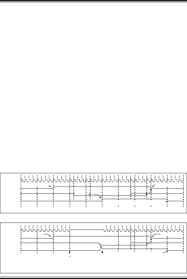
FIGURE 20-8: AUTO-WAKE-UP BIT (WUE) TIMINGS DURING NORMAL OPERATION
Q1 Q2 Q3 Q4 Q1 Q2 Q3 Q4 Q1 Q2 Q3 Q4 Q1 Q2 Q3 Q4 Q1 Q2 Q3 Q4 Q1 Q2 Q3 Q4 Q1 Q2 Q3 Q4 Q1 Q2 Q3 Q4 Q1 Q2 Q3 Q4 Q1 Q2 Q3 Q4
OSC1 |
|
|
|
Bit set by user |
|
Auto-Cleared |
|
WUE bit(1) |
|
|
|
RX/DT Line |
|
|
|
RCIF |
|
|
Cleared due to user read of RCREG |
|
|
|
|
Note 1: The EUSART remains in Idle while the WUE bit is set. |
|
|
|
FIGURE 20-9: |
AUTO-WAKE-UP BIT (WUE) TIMINGS DURING SLEEP |
||
Q1 Q2 Q3 Q4 Q1 Q2 Q3 Q4 Q1 Q2 Q3 Q4 |
Q1 |
Q2 Q3 Q4 Q1 Q2 Q3 Q4 Q1 Q2 Q3 Q4 Q1 Q2 Q3 Q4 Q1 Q2 Q3 Q4 |
|
OSC1 |
|
|
|
Bit set by user |
|
Auto-Cleared |
|
WUE bit(2) |
|
|
|
RX/DT Line |
|
|
Note 1 |
|
|
|
|
RCIF
Sleep Command Executed |
|
Sleep Ends |
|
Cleared due to user read of RCREG |
|
|
|||
|
||||
|
|
|
Note 1: If the wake-up event requires long oscillator warm-up time, the auto-clear of the WUE bit can occur before the oscillator is ready. This sequence should not depend on the presence of Q clocks.
2:The EUSART remains in Idle while the WUE bit is set.
DS39632D-page 252 |
Preliminary |
♥ 2007 Microchip Technology Inc. |