- •Universal Serial Bus Features:
- •Power-Managed Modes:
- •Flexible Oscillator Structure:
- •Peripheral Highlights:
- •Special Microcontroller Features:
- •Pin Diagrams
- •Pin Diagrams (Continued)
- •Table of Contents
- •Most Current Data Sheet
- •Errata
- •Customer Notification System
- •1.0 Device Overview
- •1.1 New Core Features
- •1.1.1 nanoWatt Technology
- •1.1.2 Universal Serial Bus (USB)
- •1.1.3 Multiple Oscillator Options and Features
- •1.2 Other Special Features
- •1.3 Details on Individual Family Members
- •FIGURE 1-2: PIC18F4455/4550 (40/44-Pin) Block Diagram
- •2.0 Oscillator Configurations
- •2.1 Overview
- •2.1.1 Oscillator Control
- •2.2 Oscillator Types
- •2.2.1 Oscillator Modes and USB Operation
- •2.2.2 Crystal Oscillator/Ceramic Resonators
- •FIGURE 2-2: Crystal/Ceramic Resonator Operation (XT, HS or HSPLL Configuration)
- •TABLE 2-1: Capacitor Selection for Ceramic Resonators
- •TABLE 2-2: Capacitor Selection for Crystal Oscillator
- •FIGURE 2-3: External Clock Input Operation (HS Osc Configuration)
- •2.2.3 External Clock Input
- •FIGURE 2-5: External Clock Input Operation (ECIO and ECPIO Configuration)
- •2.2.4 PLL Frequency Multiplier
- •FIGURE 2-6: PLL Block Diagram (HS Mode)
- •2.2.5 Internal Oscillator Block
- •2.3 Oscillator Settings for USB
- •2.3.2 Running Different USB and Microcontroller Clocks
- •2.4 Clock Sources and Oscillator Switching
- •2.4.1 Oscillator Control Register
- •2.4.2 Oscillator Transitions
- •3.0 Power-Managed Modes
- •3.1.1 Clock Sources
- •TABLE 3-1: Power-Managed Modes
- •3.1.3 Clock Transitions and Status Indicators
- •3.1.4 Multiple Sleep Commands
- •3.2 Run Modes
- •3.2.1 PRI_RUN Mode
- •3.2.2 SEC_RUN Mode
- •FIGURE 3-1: Transition Timing for Entry to SEC_RUN Mode
- •FIGURE 3-2: Transition Timing From SEC_RUN Mode to PRI_RUN Mode (HSPLL)
- •3.2.3 RC_RUN Mode
- •FIGURE 3-4: Transition Timing From RC_RUN Mode to PRI_RUN Mode
- •3.3 Sleep Mode
- •3.4 Idle Modes
- •FIGURE 3-5: Transition Timing for Entry to Sleep Mode
- •FIGURE 3-6: Transition Timing for Wake From Sleep (HSPLL)
- •3.4.1 PRI_IDLE Mode
- •3.4.2 SEC_IDLE Mode
- •FIGURE 3-7: Transition Timing for Entry to Idle Mode
- •FIGURE 3-8: Transition Timing for Wake From Idle to Run Mode
- •3.4.3 RC_IDLE Mode
- •3.5 Exiting Idle and Sleep Modes
- •3.5.1 Exit By Interrupt
- •3.5.3 Exit By Reset
- •TABLE 3-2: Exit Delay on Wake-up By Reset From Sleep Mode or Any Idle Mode (By Clock Sources)
- •4.0 Reset
- •4.1 RCON Register
- •FIGURE 4-1: Simplified Block Diagram of On-Chip Reset Circuit
- •4.2 Master Clear Reset (MCLR)
- •FIGURE 4-2: External Power-on Reset Circuit (for Slow Vdd Power-up)
- •4.4.1 Software Enabled BOR
- •4.4.2 Detecting BOR
- •4.4.3 Disabling BOR in Sleep Mode
- •TABLE 4-1: BOR Configurations
- •4.5 Device Reset Timers
- •FIGURE 4-3: Time-out Sequence on Power-up (MCLR Tied to Vdd, Vdd Rise < Tpwrt)
- •FIGURE 4-4: Time-out Sequence on Power-up (MCLR Not Tied to Vdd): Case 1
- •FIGURE 4-5: Time-out Sequence on Power-up (MCLR Not Tied to Vdd): Case 2
- •FIGURE 4-6: Slow Rise Time (MCLR Tied to Vdd, Vdd Rise > Tpwrt)
- •FIGURE 4-7: Time-out Sequence on POR w/PLL Enabled (MCLR Tied to Vdd)
- •4.6 Reset State of Registers
- •5.0 Memory Organization
- •5.1 Program Memory Organization
- •FIGURE 5-1: Program Memory Map and Stack for PIC18F2455/2550/4455/4550 Devices
- •5.1.1 Program Counter
- •5.1.2 Return Address Stack
- •FIGURE 5-2: Return Address Stack and Associated Registers
- •5.1.3 Fast Register Stack
- •5.2 PIC18 Instruction Cycle
- •5.2.1 Clocking Scheme
- •5.2.2 Instruction Flow/Pipelining
- •5.2.3 Instructions in Program Memory
- •EXAMPLE 5-4: Two-Word Instructions
- •5.3 Data Memory Organization
- •5.3.2 Bank Select Register (BSR)
- •FIGURE 5-5: Data Memory Map for PIC18F2455/2550/4455/4550 Devices
- •FIGURE 5-6: Use of the Bank Select Register (Direct Addressing)
- •5.3.3 Access Bank
- •5.3.4 General Purpose Register File
- •5.3.5 Special Function Registers
- •5.3.6 Status Register
- •5.4 Data Addressing Modes
- •5.4.1 Inherent and Literal Addressing
- •5.4.2 Direct Addressing
- •5.4.3 Indirect Addressing
- •FIGURE 5-7: Indirect Addressing
- •5.5 Program Memory and the Extended Instruction Set
- •5.6 Data Memory and the Extended Instruction Set
- •5.6.1 Indexed Addressing with Literal Offset
- •5.6.2 Instructions Affected By Indexed Literal Offset Mode
- •5.6.3 Mapping the Access Bank in Indexed Literal Offset Mode
- •5.6.4 BSR in Indexed Literal Offset Mode
- •FIGURE 5-9: Remapping the Access Bank with Indexed Literal Offset Addressing
- •6.0 Flash Program Memory
- •6.1 Table Reads and Table Writes
- •FIGURE 6-2: Table Write Operation
- •6.2 Control Registers
- •6.2.1 EECON1 and EECON2 Registers
- •6.2.2 Table Latch Register (TABLAT)
- •6.2.3 Table Pointer Register (TBLPTR)
- •6.2.4 Table Pointer Boundaries
- •FIGURE 6-3: Table Pointer Boundaries Based on Operation
- •6.3 Reading the Flash Program Memory
- •FIGURE 6-4: Reads From Flash Program Memory
- •6.4 Erasing Flash Program Memory
- •6.4.1 Flash Program Memory Erase Sequence
- •6.5 Writing to Flash Program Memory
- •FIGURE 6-5: Table Writes to Flash Program Memory
- •6.5.1 Flash Program Memory Write Sequence
- •EXAMPLE 6-3: Writing to Flash Program Memory (Continued)
- •6.5.2 Write Verify
- •6.5.3 Unexpected Termination of Write Operation
- •6.5.4 Protection Against Spurious Writes
- •6.6 Flash Program Operation During Code Protection
- •7.0 Data EEPROM Memory
- •7.1 EECON1 and EECON2 Registers
- •7.2 Reading the Data EEPROM Memory
- •7.3 Writing to the Data EEPROM Memory
- •7.4 Write Verify
- •EXAMPLE 7-1: Data EEPROM Read
- •7.6 Protection Against Spurious Write
- •7.7 Using the Data EEPROM
- •TABLE 7-1: Registers Associated with Data EEPROM Memory
- •8.0 8 x 8 Hardware Multiplier
- •8.1 Introduction
- •8.2 Operation
- •EQUATION 8-1: 16 x 16 Unsigned Multiplication Algorithm
- •EQUATION 8-2: 16 x 16 Signed Multiplication Algorithm
- •9.0 Interrupts
- •9.1 USB Interrupts
- •FIGURE 9-1: Interrupt Logic
- •9.2 INTCON Registers
- •9.3 PIR Registers
- •9.4 PIE Registers
- •9.5 IPR Registers
- •9.6 RCON Register
- •9.7 INTn Pin Interrupts
- •9.8 TMR0 Interrupt
- •9.10 Context Saving During Interrupts
- •10.0 I/O Ports
- •FIGURE 10-1: Generic I/O Port Operation
- •10.1 PORTA, TRISA and LATA Registers
- •EXAMPLE 10-1: Initializing PORTA
- •10.2 PORTB, TRISB and LATB Registers
- •EXAMPLE 10-2: Initializing PORTB
- •10.3 PORTC, TRISC and LATC Registers
- •TABLE 10-6: Summary of Registers Associated with PORTC
- •10.4 PORTD, TRISD and LATD Registers
- •10.5 PORTE, TRISE and LATE Registers
- •TABLE 10-9: PORTE I/O Summary
- •TABLE 10-10: Summary of Registers Associated with PORTE
- •11.0 Timer0 Module
- •11.1 Timer0 Operation
- •11.3 Prescaler
- •11.3.1 Switching Prescaler Assignment
- •11.4 Timer0 Interrupt
- •TABLE 11-1: Registers Associated with Timer0
- •12.0 Timer1 Module
- •12.1 Timer1 Operation
- •FIGURE 12-2: Timer1 Block Diagram (16-bit Read/Write Mode)
- •12.3 Timer1 Oscillator
- •12.3.1 Using Timer1 as a Clock Source
- •12.3.3 Timer1 Oscillator Layout Considerations
- •FIGURE 12-4: Oscillator Circuit with Grounded Guard Ring
- •12.4 Timer1 Interrupt
- •12.5 Resetting Timer1 Using the CCP Special Event Trigger
- •TABLE 12-2: Registers Associated with Timer1 as a Timer/Counter
- •13.0 Timer2 Module
- •13.1 Timer2 Operation
- •13.2 Timer2 Interrupt
- •13.3 TMR2 Output
- •TABLE 13-1: Registers Associated with Timer2 as a Timer/Counter
- •14.0 Timer3 Module
- •14.1 Timer3 Operation
- •14.3 Using the Timer1 Oscillator as the Timer3 Clock Source
- •14.4 Timer3 Interrupt
- •14.5 Resetting Timer3 Using the CCP Special Event Trigger
- •TABLE 14-1: Registers Associated with Timer3 as a Timer/Counter
- •15.0 Capture/Compare/PWM (CCP) Modules
- •Register 15-1: CCPxCON: Standard CCPx Control Register
- •15.1 CCP Module Configuration
- •15.1.1 CCP Modules and Timer Resources
- •TABLE 15-1: CCP Mode – Timer Resource
- •15.1.2 CCP2 Pin Assignment
- •TABLE 15-2: Interactions Between CCP1 and CCP2 for Timer Resources
- •15.2 Capture Mode
- •15.2.1 CCP Pin Configuration
- •15.2.2 Timer1/Timer3 Mode Selection
- •15.2.3 Software Interrupt
- •15.2.4 CCP Prescaler
- •EXAMPLE 15-1: Changing Between Capture Prescalers (CCP2 Shown)
- •FIGURE 15-1: Capture Mode Operation Block Diagram
- •15.3 Compare Mode
- •15.3.1 CCP Pin Configuration
- •15.3.2 Timer1/Timer3 Mode Selection
- •15.3.3 Software Interrupt Mode
- •15.3.4 Special Event Trigger
- •FIGURE 15-2: Compare Mode Operation Block Diagram
- •TABLE 15-3: Registers Associated with Capture, Compare, Timer1 and Timer3
- •15.4 PWM Mode
- •FIGURE 15-3: Simplified PWM Block Diagram
- •15.4.1 PWM Period
- •EQUATION 15-1:
- •15.4.2 PWM Duty Cycle
- •EQUATION 15-2:
- •EQUATION 15-3:
- •TABLE 15-4: Example PWM Frequencies and Resolutions at 40 MHz
- •15.4.4 Setup for PWM Operation
- •16.0 Enhanced Capture/Compare/PWM (ECCP) Module
- •Register 16-1: CCP1CON: ECCP Control Register (40/44-Pin Devices)
- •16.1 ECCP Outputs and Configuration
- •16.1.1 ECCP Modules and Timer Resources
- •16.2 Capture and Compare Modes
- •16.2.1 Special Event Trigger
- •16.3 Standard PWM Mode
- •TABLE 16-1: Pin Assignments for Various ECCP1 Modes
- •16.4 Enhanced PWM Mode
- •16.4.1 PWM Period
- •EQUATION 16-1:
- •FIGURE 16-1: Simplified Block Diagram of the Enhanced PWM Module
- •16.4.2 PWM Duty Cycle
- •EQUATION 16-2:
- •EQUATION 16-3:
- •16.4.3 PWM Output Configurations
- •TABLE 16-2: Example PWM Frequencies and Resolutions at 40 MHz
- •FIGURE 16-2: PWM Output Relationships (Active-High State)
- •FIGURE 16-3: PWM Output Relationships (Active-Low State)
- •FIGURE 16-4: Half-Bridge PWM Output
- •FIGURE 16-5: Examples of Half-Bridge Output Mode Applications
- •FIGURE 16-6: Full-Bridge PWM Output
- •FIGURE 16-7: Example of Full-Bridge Application
- •FIGURE 16-9: PWM Direction Change at Near 100% Duty Cycle
- •Register 16-2: ECCP1DEL: PWM Dead-Band Delay Register
- •Register 16-3: ECCP1AS: Enhanced Capture/Compare/PWM Auto-Shutdown Control Register
- •FIGURE 16-10: PWM Auto-Shutdown (PRSEN = 1, Auto-Restart Enabled)
- •FIGURE 16-11: PWM Auto-Shutdown (PRSEN = 0, Auto-Restart Disabled)
- •16.4.9 Setup for PWM Operation
- •16.4.11 Effects of a Reset
- •TABLE 16-3: Registers Associated with ECCP Module And Timer1 to Timer3
- •17.0 Universal Serial Bus (USB)
- •17.1 Overview of the USB Peripheral
- •17.2 USB Status and Control
- •17.2.1 USB Control Register (UCON)
- •Register 17-1: UCON: USB Control Register
- •17.2.2 USB Configuration Register (UCFG)
- •FIGURE 17-2: Typical External Transceiver with Isolation
- •Register 17-2: UCFG: USB Configuration Register
- •FIGURE 17-3: External Circuitry
- •17.2.3 USB Status Register (USTAT)
- •Register 17-3: USTAT: USB Status Register
- •17.2.4 USB Endpoint Control
- •Register 17-4: UEPn: USB Endpoint n Control Register (UEP0 Through UEP15)
- •17.2.5 USB Address Register (UADDR)
- •17.2.6 USB Frame Number Registers (UFRMH:UFRML)
- •FIGURE 17-5: Implementation of USB RAM in Data Memory Space
- •17.4 Buffer Descriptors and the Buffer Descriptor Table
- •17.4.1 BD Status and Configuration
- •FIGURE 17-6: Example of a Buffer Descriptor
- •TABLE 17-3: Effect of DTSEN Bit on Odd/Even (DATA0/DATA1) Packet Reception
- •17.4.2 BD Byte Count
- •17.4.3 BD Address Validation
- •FIGURE 17-7: Buffer Descriptor Table Mapping for Buffering Modes
- •TABLE 17-4: Assignment of Buffer Descriptors for the Different Buffering Modes
- •TABLE 17-5: Summary of USB Buffer Descriptor Table Registers
- •17.5 USB Interrupts
- •17.5.1 USB Interrupt Status Register (UIR)
- •Register 17-7: UIR: USB Interrupt Status Register
- •EXAMPLE 17-1: Clearing ACTVIF Bit (UIR<2>)
- •17.5.2 USB Interrupt Enable Register (UIE)
- •Register 17-8: UIE: USB Interrupt Enable Register
- •17.5.3 USB Error Interrupt Status Register (UEIR)
- •Register 17-9: UEIR: USB Error Interrupt Status Register
- •17.5.4 USB Error Interrupt Enable Register (UEIE)
- •Register 17-10: UEIE: USB Error Interrupt Enable Register
- •17.6 USB Power Modes
- •17.6.1 Bus Power Only
- •FIGURE 17-10: Bus Power Only
- •FIGURE 17-11: Self-power Only
- •FIGURE 17-12: Dual Power Example
- •17.7 Streaming Parallel Port
- •17.8 Oscillator
- •17.9 USB Firmware and Drivers
- •TABLE 17-6: Registers Associated with USB Module Operation(1)
- •17.10 Overview of USB
- •17.10.1 Layered Framework
- •17.10.2 Frames
- •17.10.3 Transfers
- •17.10.4 Power
- •FIGURE 17-13: USB Layers
- •17.10.5 Enumeration
- •17.10.6 Descriptors
- •17.10.7 Bus Speed
- •17.10.8 Class Specifications and Drivers
- •18.0 Streaming Parallel Port
- •18.1 SPP Configuration
- •18.1.1 Enabling the SPP
- •Register 18-1: SPPCON: SPP Control Register
- •Register 18-2: SPPCFG: SPP Configuration Register
- •18.1.2 Clocking Data
- •18.1.3 Wait States
- •FIGURE 18-2: Timing for Microcontroller Write Address, Write Data and Read Data (No Wait States)
- •FIGURE 18-3: Timing for USB Write Address and Data (4 Wait States)
- •FIGURE 18-4: Timing for USB Write Address and Read Data (4 Wait States)
- •18.2 Setup for USB Control
- •18.3 Setup for Microcontroller Control
- •18.3.1 SPP Interrupts
- •18.3.2 Writing to the SPP
- •FIGURE 18-5: Transfer of Data Between USB SIE and SPP
- •18.3.3 Reading From the SPP
- •Register 18-3: SPPEPS: SPP Endpoint Address and Status Register
- •TABLE 18-1: Registers Associated with the Streaming Parallel Port
- •19.0 Master Synchronous Serial Port (MSSP) Module
- •19.1 Master SSP (MSSP) Module Overview
- •19.2 Control Registers
- •19.3 SPI Mode
- •19.3.1 Registers
- •Register 19-2: SSPCON1: MSSP Control Register 1 (SPI Mode)
- •19.3.2 Operation
- •19.3.3 Enabling SPI I/O
- •19.3.4 Typical Connection
- •19.3.5 Master Mode
- •FIGURE 19-3: SPI Mode Waveform (Master Mode)
- •19.3.6 Slave Mode
- •19.3.7 Slave Select Synchronization
- •FIGURE 19-4: Slave Synchronization Waveform
- •FIGURE 19-5: SPI Mode Waveform (Slave Mode with CKE = 0)
- •FIGURE 19-6: SPI Mode Waveform (Slave Mode with CKE = 1)
- •19.3.9 Effects of a Reset
- •19.3.10 Bus Mode Compatibility
- •TABLE 19-1: SPI Bus Modes
- •TABLE 19-2: Registers Associated with SPI Operation
- •FIGURE 19-7: MSSP Block Diagram (I2C™ Mode)
- •19.4.1 Registers
- •19.4.2 Operation
- •19.4.3 Slave Mode
- •EXAMPLE 19-2: Address Masking Examples
- •19.4.4 Clock Stretching
- •FIGURE 19-14: Clock Synchronization Timing
- •19.4.5 General Call Address Support
- •FIGURE 19-17: Slave Mode General Call Address Sequence (7 or 10-Bit Address Mode)
- •19.4.6 Master Mode
- •FIGURE 19-18: MSSP Block Diagram (I2C™ Master Mode)
- •19.4.7 Baud Rate
- •FIGURE 19-19: Baud Rate Generator Block Diagram
- •TABLE 19-3: I2C™ Clock Rate w/BRG
- •FIGURE 19-20: Baud Rate Generator Timing with Clock Arbitration
- •FIGURE 19-21: First Start Bit Timing
- •FIGURE 19-22: Repeated Start Condition Waveform
- •19.4.12 Acknowledge Sequence Timing
- •19.4.13 Stop Condition Timing
- •FIGURE 19-25: Acknowledge Sequence Waveform
- •FIGURE 19-26: Stop Condition Receive or Transmit Mode
- •19.4.14 Sleep Operation
- •19.4.15 EffectS of a Reset
- •FIGURE 19-27: Bus Collision Timing for Transmit and Acknowledge
- •FIGURE 19-28: Bus Collision During Start Condition (SDA Only)
- •FIGURE 19-29: Bus Collision During Start Condition (SCL = 0)
- •FIGURE 19-30: BRG Reset Due to SDA Arbitration During Start Condition
- •FIGURE 19-31: Bus Collision During a Repeated Start Condition (Case 1)
- •FIGURE 19-32: Bus Collision During Repeated Start Condition (Case 2)
- •FIGURE 19-33: Bus Collision During a Stop Condition (Case 1)
- •FIGURE 19-34: Bus Collision During a Stop Condition (Case 2)
- •TABLE 19-4: Registers Associated with I2C™ Operation
- •20.0 Enhanced Universal Synchronous Asynchronous Receiver Transmitter (EUSART)
- •20.1 Baud Rate Generator (BRG)
- •20.1.2 Sampling
- •TABLE 20-1: Baud Rate Formulas
- •EXAMPLE 20-1: Calculating Baud Rate Error
- •TABLE 20-2: Registers Associated with Baud Rate Generator
- •FIGURE 20-1: Automatic Baud Rate Calculation
- •FIGURE 20-2: BRG Overflow Sequence
- •20.2 EUSART Asynchronous Mode
- •20.2.1 EUSART Asynchronous Transmitter
- •FIGURE 20-3: EUSART Transmit Block Diagram
- •FIGURE 20-4: Asynchronous Transmission, TXCKP = 0 (TX Not Inverted)
- •TABLE 20-5: Registers Associated with Asynchronous Transmission
- •20.2.2 EUSART Asynchronous Receiver
- •FIGURE 20-6: EUSART Receive Block Diagram
- •FIGURE 20-7: Asynchronous Reception, RXDTP = 0 (RX Not Inverted)
- •FIGURE 20-8: Auto-Wake-up Bit (WUE) Timings During Normal Operation
- •20.2.5 Break Character Sequence
- •20.2.6 Receiving A Break Character
- •FIGURE 20-10: Send Break Character Sequence
- •20.3 EUSART Synchronous Master Mode
- •20.3.1 EUSART Synchronous Master Transmission
- •FIGURE 20-11: Synchronous Transmission
- •FIGURE 20-12: Synchronous Transmission (Through TXEN)
- •20.3.2 EUSART Synchronous Master Reception
- •FIGURE 20-13: Synchronous Reception (Master Mode, SREN)
- •TABLE 20-8: Registers Associated with Synchronous Master Reception
- •20.4 EUSART Synchronous Slave Mode
- •20.4.1 EUSART Synchronous Slave Transmission
- •TABLE 20-9: Registers Associated with Synchronous Slave Transmission
- •20.4.2 EUSART Synchronous Slave Reception
- •TABLE 20-10: Registers Associated with Synchronous Slave Reception
- •21.1 A/D Acquisition Requirements
- •EQUATION 21-1: Acquisition Time
- •EQUATION 21-2: A/D Minimum Charging Time
- •EQUATION 21-3: Calculating the Minimum Required Acquisition Time
- •21.2 Selecting and Configuring Acquisition Time
- •21.3 Selecting the A/D Conversion Clock
- •TABLE 21-1: Tad vs. Device Operating Frequencies
- •21.5 Configuring Analog Port Pins
- •21.6 A/D Conversions
- •21.7 Discharge
- •FIGURE 21-4: A/D Conversion Tad Cycles (ACQT<2:0> = 000, Tacq = 0)
- •21.8 Use of the CCP2 Trigger
- •TABLE 21-2: Registers Associated with A/D Operation
- •22.0 Comparator Module
- •22.1 Comparator Configuration
- •22.2 Comparator Operation
- •22.3 Comparator Reference
- •FIGURE 22-2: Single Comparator
- •22.3.1 External Reference Signal
- •22.3.2 Internal Reference Signal
- •22.4 Comparator Response Time
- •22.5 Comparator Outputs
- •FIGURE 22-3: Comparator Output Block Diagram
- •22.6 Comparator Interrupts
- •22.7 Comparator Operation During Sleep
- •22.8 Effects of a Reset
- •22.9 Analog Input Connection Considerations
- •TABLE 22-1: Registers Associated with Comparator Module
- •23.0 Comparator Voltage Reference Module
- •23.1 Configuring the Comparator Voltage Reference
- •FIGURE 23-1: Comparator Voltage Reference Block Diagram
- •23.2 Voltage Reference Accuracy/Error
- •23.3 Operation During Sleep
- •23.4 Effects of a Reset
- •23.5 Connection Considerations
- •FIGURE 23-2: Comparator Voltage Reference Output Buffer Example
- •24.1 Operation
- •FIGURE 24-1: HLVD Module Block Diagram (with External Input)
- •24.2 HLVD Setup
- •24.3 Current Consumption
- •FIGURE 24-2: Low-Voltage Detect Operation (VDIRMAG = 0)
- •FIGURE 24-3: High-Voltage Detect Operation (VDIRMAG = 1)
- •24.5 Applications
- •24.6 Operation During Sleep
- •24.7 Effects of a Reset
- •TABLE 24-1: Registers Associated with High/Low-Voltage Detect Module
- •25.0 Special Features of the CPU
- •25.1 Configuration Bits
- •TABLE 25-1: Configuration Bits and Device IDs
- •Register 25-5: CONFIG3H: Configuration Register 3 High (Byte Address 300005h)
- •Register 25-6: CONFIG4L: Configuration Register 4 Low (Byte Address 300006h)
- •Register 25-7: CONFIG5L: Configuration Register 5 Low (Byte Address 300008h)
- •Register 25-8: CONFIG5H: Configuration Register 5 High (Byte Address 300009h)
- •Register 25-9: CONFIG6L: Configuration Register 6 Low (Byte Address 30000Ah)
- •Register 25-10: CONFIG6H: Configuration Register 6 High (Byte Address 30000Bh)
- •Register 25-11: CONFIG7L: Configuration Register 7 Low (Byte Address 30000Ch)
- •Register 25-12: CONFIG7H: Configuration Register 7 High (Byte Address 30000Dh)
- •Register 25-13: DEVID1: Device ID Register 1 for PIC18F2455/2550/4455/4550 Devices
- •Register 25-14: DEVID2: Device ID Register 2 for PIC18F2455/2550/4455/4550 Devices
- •25.2 Watchdog Timer (WDT)
- •25.2.1 Control Register
- •FIGURE 25-1: WDT Block Diagram
- •Register 25-15: WDTCON: Watchdog Timer Control Register
- •TABLE 25-2: Summary of Watchdog Timer Registers
- •25.3 Two-Speed Start-up
- •FIGURE 25-2: Timing Transition for Two-Speed Start-up (INTOSC to HSPLL)
- •FIGURE 25-3: FSCM Block Diagram
- •25.4.1 FSCM and the Watchdog Timer
- •FIGURE 25-4: FSCM Timing Diagram
- •25.5 Program Verification and Code Protection
- •TABLE 25-3: Summary of Code Protection Registers
- •25.5.1 Program Memory Code Protection
- •FIGURE 25-7: External Block Table Read (EBTRn) Disallowed
- •FIGURE 25-8: External Block Table Read (EBTRn) Allowed
- •25.5.2 Data EEPROM Code Protection
- •25.5.3 Configuration Register Protection
- •25.6 ID Locations
- •TABLE 25-4: Debugger Resources
- •25.9 Special ICPORT Features (Designated Packages Only)
- •25.9.1 Dedicated ICD/ICSP Port
- •TABLE 25-5: Equivalent Pins for Legacy and Dedicated ICD/ICSP™ Ports
- •25.10 Single-Supply ICSP Programming
- •26.0 Instruction Set Summary
- •26.1 Standard Instruction Set
- •TABLE 26-1: Opcode Field Descriptions
- •FIGURE 26-1: General Format for Instructions
- •26.1.1 Standard Instruction Set
- •26.2 Extended Instruction Set
- •26.2.1 Extended Instruction Syntax
- •TABLE 26-3: Extensions to the PIC18 Instruction Set
- •26.2.2 Extended Instruction Set
- •26.2.4 Considerations When Enabling the Extended Instruction Set
- •27.0 Development Support
- •27.1 MPLAB Integrated Development Environment Software
- •27.2 MPASM Assembler
- •27.3 MPLAB C18 and MPLAB C30 C Compilers
- •27.4 MPLINK Object Linker/ MPLIB Object Librarian
- •27.5 MPLAB ASM30 Assembler, Linker and Librarian
- •27.6 MPLAB SIM Software Simulator
- •27.10 MPLAB PM3 Device Programmer
- •27.11 PICSTART Plus Development Programmer
- •27.12 Demonstration, Development and Evaluation Boards
- •28.0 Electrical Characteristics
- •Absolute Maximum Ratings(†)
- •FIGURE 28-1: PIC18F2455/2550/4455/4550 Voltage-Frequency Graph (Industrial)
- •FIGURE 28-2: PIC18LF2455/2550/4455/4550 Voltage-Frequency Graph (Industrial)
- •TABLE 28-2: Comparator Specifications
- •TABLE 28-3: Voltage Reference Specifications
- •TABLE 28-4: USB Module Specifications
- •TABLE 28-5: USB Internal Voltage Regulator Specifications
- •FIGURE 28-3: High/Low-Voltage Detect Characteristics
- •TABLE 28-6: High/Low-Voltage Detect Characteristics
- •28.4 AC (Timing) Characteristics
- •28.4.1 Timing Parameter Symbology
- •28.4.2 Timing Conditions
- •TABLE 28-7: Temperature and Voltage Specifications – AC
- •FIGURE 28-4: Load Conditions for Device Timing Specifications
- •28.4.3 Timing Diagrams And Specifications
- •FIGURE 28-5: External Clock Timing (All Modes Except PLL)
- •TABLE 28-8: External Clock Timing Requirements
- •TABLE 28-9: PLL Clock Timing Specifications (Vdd = 3.0V to 5.5V)
- •FIGURE 28-6: CLKO and I/O Timing
- •TABLE 28-11: CLKO and I/O Timing Requirements
- •FIGURE 28-7: Reset, Watchdog Timer, Oscillator Start-up Timer and Power-up Timer Timing
- •FIGURE 28-9: Timer0 and Timer1 External Clock Timings
- •TABLE 28-13: Timer0 and Timer1 External Clock Requirements
- •FIGURE 28-10: Capture/Compare/PWM Timings (All CCP Modules)
- •TABLE 28-14: Capture/Compare/PWM Requirements (All CCP Modules)
- •FIGURE 28-15: I2C™ Bus Start/Stop Bits Timing
- •TABLE 28-19: I2C™ Bus Start/Stop Bits Requirements (Slave Mode)
- •FIGURE 28-16: I2C™ Bus Data Timing
- •TABLE 28-20: I2C™ Bus Data Requirements (Slave Mode)
- •FIGURE 28-17: Master SSP I2C™ Bus Start/Stop Bits Timing Waveforms
- •TABLE 28-21: Master SSP I2C™ Bus Start/Stop Bits Requirements
- •FIGURE 28-18: Master SSP I2C™ Bus Data Timing
- •TABLE 28-22: Master SSP I2C™ Bus Data Requirements
- •FIGURE 28-19: EUSART Synchronous Transmission (Master/Slave) Timing
- •TABLE 28-23: EUSART Synchronous Transmission Requirements
- •FIGURE 28-20: EUSART Synchronous Receive (Master/Slave) Timing
- •TABLE 28-24: EUSART Synchronous Receive Requirements
- •FIGURE 28-21: USB Signal Timing
- •TABLE 28-25: USB Low-Speed Timing Requirements
- •TABLE 28-26: USB Full-Speed Requirements
- •FIGURE 28-22: Streaming Parallel Port Timing (PIC18F4455/4550)
- •TABLE 28-27: Streaming Parallel Port Requirements (PIC18F4455/4550)
- •FIGURE 28-23: A/D Conversion Timing
- •TABLE 28-29: A/D Conversion Requirements
- •29.0 DC and AC Characteristics Graphs and Tables
- •30.0 Packaging Information
- •30.1 Package Marking Information
- •Package Marking Information (Continued)
- •30.2 Package Details
- •Appendix A: Revision History
- •Revision A (May 2004)
- •Revision B (October 2004)
- •Revision C (February 2006)
- •Revision D (January 2007)
- •Appendix B: Device Differences
- •Appendix C: Conversion Considerations
- •Appendix D: Migration From Baseline to Enhanced Devices
- •Appendix E: Migration From Mid-Range to Enhanced Devices
- •Appendix F: Migration From High-End to Enhanced Devices
- •INDEX
- •The Microchip Web Site
- •Customer Change Notification Service
- •Customer Support
- •Reader Response
- •PIC18F2455/2550/4455/4550 Product Identification System
- •Worldwide Sales and Service
PIC18F2455/2550/4455/4550
5.4Data Addressing Modes
Note: The execution of some instructions in the core PIC18 instruction set are changed when the PIC18 extended instruction set is enabled. See Section 5.6 “Data
Memory and the Extended Instruction Set” for more information.
While the program memory can be addressed in only one way – through the program counter – information in the data memory space can be addressed in several ways. For most instructions, the addressing mode is fixed. Other instructions may use up to three modes, depending on which operands are used and whether or not the extended instruction set is enabled.
The addressing modes are:
•Inherent
•Literal
•Direct
•Indirect
An additional addressing mode, Indexed Literal Offset, is available when the extended instruction set is enabled (XINST Configuration bit = 1). Its operation is discussed in greater detail in Section 5.6.1 “Indexed Addressing with Literal Offset”.
5.4.1INHERENT AND LITERAL ADDRESSING
Many PIC18 control instructions do not need any argument at all; they either perform an operation that globally affects the device or they operate implicitly on one register. This addressing mode is known as Inherent Addressing. Examples include SLEEP, RESET and DAW.
Other instructions work in a similar way but require an additional explicit argument in the opcode. This is known as Literal Addressing mode because they require some literal value as an argument. Examples include ADDLW and MOVLW, which respectively, add or move a literal value to the W register. Other examples include CALL and GOTO, which include a 20-bit program memory address.
5.4.2DIRECT ADDRESSING
Direct Addressing mode specifies all or part of the source and/or destination address of the operation within the opcode itself. The options are specified by the arguments accompanying the instruction.
In the core PIC18 instruction set, bit-oriented and byte-oriented instructions use some version of Direct Addressing by default. All of these instructions include some 8-bit literal address as their Least Significant Byte. This address specifies either a register address in one of the banks of data RAM (Section 5.3.4 “General
Purpose Register File”) or a location in the Access Bank (Section 5.3.3 “Access Bank”) as the data source for the instruction.
The Access RAM bit ‘a’ determines how the address is interpreted. When ‘a’ is ‘1’, the contents of the BSR (Section 5.3.2 “Bank Select Register (BSR)”) are used with the address to determine the complete 12-bit address of the register. When ‘a’ is ‘0’, the address is interpreted as being a register in the Access Bank. Addressing that uses the Access RAM is sometimes also known as Direct Forced Addressing mode.
A few instructions, such as MOVFF, include the entire 12-bit address (either source or destination) in their opcodes. In these cases, the BSR is ignored entirely.
The destination of the operation’s results is determined by the destination bit ‘d’. When ‘d’ is ‘1’, the results are stored back in the source register, overwriting its original contents. When ‘d’ is ‘0’, the results are stored in the W register. Instructions without the ‘d’ argument have a destination that is implicit in the instruction; their destination is either the target register being operated on or the W register.
5.4.3INDIRECT ADDRESSING
Indirect Addressing allows the user to access a location in data memory without giving a fixed address in the instruction. This is done by using File Select Registers (FSRs) as pointers to the locations to be read or written to. Since the FSRs are themselves located in RAM as Special Function Registers, they can also be directly manipulated under program control. This makes FSRs very useful in implementing data structures, such as tables and arrays in data memory.
The registers for Indirect Addressing are also implemented with Indirect File Operands (INDFs) that permit automatic manipulation of the pointer value with auto-incrementing, auto-decrementing or offsetting with another value. This allows for efficient code, using loops, such as the example of clearing an entire RAM bank in Example 5-5.
EXAMPLE 5-5: |
HOW TO CLEAR RAM |
|
|
(BANK 1) USING |
|
|
INDIRECT ADDRESSING |
|
LFSR |
FSR0, 100h |
; |
NEXT CLRF |
POSTINC0 |
; Clear INDF |
|
|
; register then |
|
|
; inc pointer |
BTFSS |
FSR0H, 1 |
; All done with |
|
|
; Bank1? |
BRA |
NEXT |
; NO, clear next |
CONTINUE |
|
; YES, continue |
|
|
|
DS39632D-page 72 |
Preliminary |
♥ 2007 Microchip Technology Inc. |
PIC18F2455/2550/4455/4550
5.4.3.1FSR Registers and the INDF Operand
At the core of Indirect Addressing are three sets of registers: FSR0, FSR1 and FSR2. Each represents a pair of 8-bit registers: FSRnH and FSRnL. The four upper bits of the FSRnH register are not used, so each FSR pair holds a 12-bit value. This represents a value that can address the entire range of the data memory in a linear fashion. The FSR register pairs, then, serve as pointers to data memory locations.
Indirect Addressing is accomplished with a set of Indirect File Operands, INDF0 through INDF2. These can be thought of as “virtual” registers; they are
mapped in the SFR space but are not physically implemented. Reading or writing to a particular INDF register actually accesses its corresponding FSR register pair. A read from INDF1, for example, reads the data at the address indicated by FSR1H:FSR1L. Instructions that use the INDF registers as operands actually use the contents of their corresponding FSR as a pointer to the instruction’s target. The INDF operand is just a convenient way of using the pointer.
Because Indirect Addressing uses a full 12-bit address, data RAM banking is not necessary. Thus, the current contents of the BSR and the Access RAM bit have no effect on determining the target address.
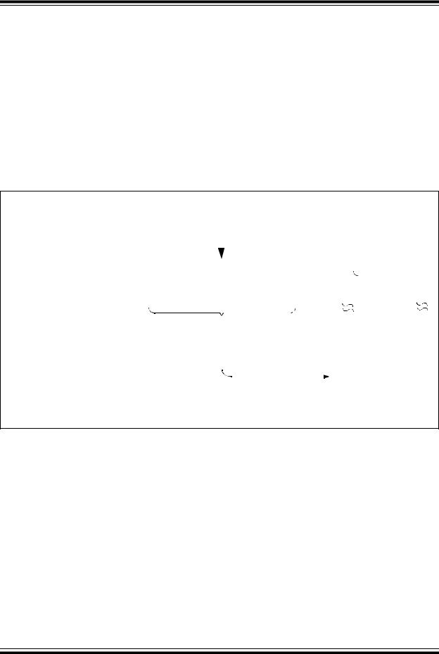
FIGURE 5-7: INDIRECT ADDRESSING
Using an instruction with one of the indirect addressing registers as the operand....
...uses the 12-bit address stored in the FSR pair associated with that register....
...to determine the data memory location to be used in that operation.
In this case, the FSR1 pair contains ECCh. This means the contents of location ECCh will be added to that of the W register and stored back in ECCh.
|
|
|
|
|
|
|
|
|
|
|
|
|
|
|
|
|
|
|
|
|
000h |
|
|
|
|
|
|
ADDWF, INDF1, 1 |
|
|
|
|
|
|
Bank 0 |
||||||||||||
|
|
|
|
|
|
|
|
|
|
|
|
||||||||||||
|
|
|
|
|
|
|
|
|
|
|
|
|
|
|
|
|
|
|
|
|
100h |
|
|
|
|
|
|
|
|
|
|
|
|
|
|
|
|
|
|
|
|
|
|
|
Bank 1 |
||
|
|
|
|
|
|
|
|
|
|
|
|
|
|
|
|
|
|
|
|
|
|
|
|
|
|
|
|
|
|
|
|
|
|
|
|
|
|
|
|
|
|
|
|
|
200h |
|
|
|
|
|
|
|
|
|
|
|
|
|
|
|
|
|
|
|
|
|
|
|
Bank 2 |
||
|
|
|
|
|
|
|
|
|
|
|
|
|
|
|
|
|
|
|
|
|
300h |
|
|
|
|
|
|
|
FSR1H:FSR1L |
|
|
|
|
|
|
|
|
||||||||||
|
|
|
|
|
|
|
|
|
|
|
|
|
|
||||||||||
7 |
|
|
|
0 |
|
7 |
|
|
|
0 |
|
|
|
|
|||||||||
|
|
|
|
|
|
|
|
|
|
|
|
|
|
|
|
|
|
|
|
|
|
|
|
x |
x |
x |
x |
1 |
1 |
1 |
0 |
|
|
1 |
1 |
0 |
0 |
1 |
1 |
0 |
0 |
|
|
|
Bank 3 |
||
|
|
|
|
|
|
|
|
|
|
|
|
|
|
|
|
|
|
|
|
|
|
|
|
|
|
|
|
|
|
|
|
|
|
|
|
|
|
|
|
|
|
|
|
|
|
|
through |
|
|
|
|
|
|
|
|
|
|
|
|
|
|
|
|
|
|
|
|
|
E00h |
Bank 13 |
|
|
|
|
|
|
|
|
|
|
|
|
|
|
|
|
|
|
|
|
|
|
|||
|
|
|
|
|
|
|
|
|
|
|
|
|
|
|
|
|
|
|
|
|
|
||
|
|
|
|
|
|
|
|
|
|
|
|
|
|
|
|
|
|
|
|
|
Bank 14 |
||
|
|
|
|
|
|
|
|
|
|
|
|
|
|
|
|
|
|
|
|
|
F00h |
||
|
|
|
|
|
|
|
|
|
|
|
|
|
|
|
|
|
|
|
|
|
|||
|
|
|
|
|
|
|
|
|
|
|
|
|
|
|
|
|
|
|
|
|
|
||
|
|
|
|
|
|
|
|
|
|
|
|
|
|
|
|
|
|
|
|
|
Bank 15 |
||
|
|
|
|
|
|
|
|
|
|
|
|
|
|
|
|
|
|
|
|
|
FFFh |
||
|
|
|
|
|
|
|
|
|
|
|
|
|
|
|
|
|
|
|
|
|
|
Data Memory
♥ 2007 Microchip Technology Inc. |
Preliminary |
DS39632D-page 73
PIC18F2455/2550/4455/4550
5.4.3.2FSR Registers and POSTINC, POSTDEC, PREINC and PLUSW
In addition to the INDF operand, each FSR register pair also has four additional indirect operands. Like INDF, these are “virtual” registers that cannot be indirectly read or written to. Accessing these registers actually accesses the associated FSR register pair, but also performs a specific action on it stored value. They are:
•POSTDEC: accesses the FSR value, then automatically decrements it by ‘1’ afterwards
•POSTINC: accesses the FSR value, then automatically increments it by ‘1’ afterwards
•PREINC: increments the FSR value by ‘1’, then uses it in the operation
•PLUSW: adds the signed value of the W register (range of -127 to 128) to that of the FSR and uses the new value in the operation.
In this context, accessing an INDF register uses the value in the FSR registers without changing them. Similarly, accessing a PLUSW register gives the FSR value offset by that in the W register; neither value is actually changed in the operation. Accessing the other virtual registers changes the value of the FSR registers.
Operations on the FSRs with POSTDEC, POSTINC and PREINC affect the entire register pair; that is, rollovers of the FSRnL register, from FFh to 00h, carry over to the FSRnH register. On the other hand, results of these operations do not change the value of any flags in the STATUS register (e.g., Z, N, OV, etc.).
The PLUSW register can be used to implement a form of Indexed Addressing in the data memory space. By manipulating the value in the W register, users can reach addresses that are fixed offsets from pointer addresses. In some applications, this can be used to implement some powerful program control structure, such as software stacks, inside of data memory.
5.4.3.3Operations by FSRs on FSRs
Indirect Addressing operations that target other FSRs or virtual registers represent special cases. For example, using an FSR to point to one of the virtual registers will not result in successful operations. As a specific case, assume that FSR0H:FSR0L contains FE7h, the address of INDF1. Attempts to read the value of INDF1, using INDF0 as an operand, will return 00h. Attempts to write to INDF1, using INDF0 as the operand, will result in a NOP.
On the other hand, using the virtual registers to write to an FSR pair may not occur as planned. In these cases, the value will be written to the FSR pair but without any incrementing or decrementing. Thus, writing to INDF2 or POSTDEC2 will write the same value to the FSR2H:FSR2L.
Since the FSRs are physical registers mapped in the SFR space, they can be manipulated through all direct operations. Users should proceed cautiously when working on these registers, particularly if their code uses Indirect Addressing.
Similarly, operations by Indirect Addressing are generally permitted on all other SFRs. Users should exercise the appropriate caution that they do not inadvertently change settings that might affect the operation of the device.
DS39632D-page 74 |
Preliminary |
♥ 2007 Microchip Technology Inc. |