

Micro-Cap v7.1.6 / RM
.PDFThe Active Filter dialog box
The active filter designer is located on the Design menu. Selecting this menu invokes the following dialog box:
Figure 12-1 The Active Filter dialog box
This dialog box has three main panels, accessible by clicking on a named tab.
Design
This panel lets you pick the filter type, specifications, and the response characteristic. Each time you change one of these selections the number of stages, the pole location, Q value, and, depending upon the response type, the zeros of each stage are calculated and shown in the Poles and Zeros display. You can edit the F0 (pole frequency), Q0 (Q value), and FN (zero frequency) values to change the shape of the response.
Implementation
This panel lets you make the implementation decisions, including which circuit to use, whether to use exact passive component values or to select them from specified lists, which OPAMPs to use, and how to build the odd order stages.
167
Options
In this panel you choose the number of digits of precision to be used in the component values, what to plot, whether to create a macro or a circuit, and whether to use an existing circuit or a new one.
Design Panel: The main panel contains three sections:
Type: This section lets you select one of the five basic types of filters:
•Low pass
•High pass
•Bandpass
•Notch
•Delay
Response: This section lets you select the mathematical approximation to the ideal filter.
•Butterworth
•Chebyshev
•Bessel
•Elliptic
•Inverse-Chebyshev
Different responses provide different design trade-offs. Butterworth filters require much more circuitry for a given specification, but have a flatter time delay response. Chebyshev and inverse-Chebyshev responses require fewer stages, but have a more pronounced time delay variation. Elliptic responses require the fewest number of stages, but generate the greatest delay variation. Bessel filters are low pass filters with a very flat time delay curve and are really suitable only for delay types. The number of stages to implement the current design is shown to the right of each response.
Specifications: This is where you enter the numerical specifications of the filter. There are two ways to specify a filter, Mode 1 and Mode 2. In Mode 1, you specify the functional characteristics of the filter, like passband gain, cutoff frequency, stop frequency, and attenuation. You specify what you want and the program figures out the number of stages required to achieve it, using the specified response approximation. Mode 2, on the other hand, lets you directly specify the main design values and the number of stages directly.
168 Chapter 12: Active Filter Designer
Poles and Zeros: This section shows the numeric values of the poles, zeros, and Qs of the response polynomial. It essentially shows the mathematical design of the filter. When you make a change to the Type, Response, or Specifications fields, the program redesigns the polynomial coefficients and updates the numbers in this section. If the Plot button has been clicked, the program also redraws the response plot. It may be a Bode plot with gain, phase, and group delay shown, or it may be just a delay plot, depending upon the selections in the Options panel.
The plot is idealized because it is based on a standard polynomial formula for the selected response and the calculated or edited F0, Q0, and QN values. Its plot can only be achieved exactly with perfect components. The actual filter, made from real components, may behave differently. When the circuit is completed, you can run an analysis and see how well it fares. The actual circuit can be constructed from any opamp in the library ranging from ideal to ordinary and from resistors and capacitors that are either exact or chosen from a list of standard values. Real OPAMPs and approximate component values can have a profound effect on the response curves.
You can edit the values, to see their effect on the plot. You can even create your filter with modified values. Though this will not produce an ideal filter, the circuit created will approximate the plot shown. Note that editing any item in the Type, Response, or Specifications areas will cause the program to recalculate the values in the Poles and Zeros section, overwriting your edits.
The exact form of the approximating polynomials for each stage is shown below. Note that U is the complex frequency variable S, normalized to the specified FC.
Definitions
Symbol Definition
F |
Frequency variable |
|
S |
J*2*PI*F |
Complex frequency |
U |
S / (2*PI*FC) = J*F/FC |
Normalized complex frequency |
F0 |
Pole location in Hz |
|
Q0 |
Q value |
|
FN |
Zero location in Hz (Elliptic and inverse Chebyshev filters only) |
|
169
|
FC |
Stopband frequency for low-pass filters. Passband frequency for |
|
|
|
high-pass filters. Center frequency for bandpass and notch filters. |
|
|
|
The specified center frequency may be changed slightly to produce a |
|
|
|
symmetrical band pass/reject region. The adjusted F0 can be seen in |
|
|
|
the define statement. For example, a Butterworth bandpass filter |
|
|
|
using the default center frequency of 1000, and bandwidth of 100, is |
|
|
|
actually designed with a center frequency of 998.75 Hz. |
|
|
FCI |
Passband frequency for low-pass filters. Stopband frequency for |
|
|
|
high-pass filters. For bandpass and notch filters FCI = FC |
|
|
W0 |
F0/FC |
Normalized pole frequency |
|
W0I |
F0/FCI |
Inverse Chebyshev normalized pole frequency |
|
WN |
FN/FC |
Normalized zero frequency |
|
WNI |
FN/FCI |
Inverse Chebyshev normalized zero frequency |
|
Low Pass and Delay |
||
|
Butterworth |
F(U) = 1 / (U2 +U/Q0 + 1) |
|
|
Chebyshev |
F(U) = 1 / (U2 +U*W0/Q0 + W02) |
|
|
Elliptic |
|
F(U) = (U2+WN2) / (U2 +U*W0/Q0 + W02) |
|
Inv. Chebyshev F(U) = (U2+WNI2) / (U2 +U*W0I/Q0 + W0I2) |
||
|
High Pass |
|
|
|
Butterworth |
F(U) = U2 / (U2 +U/Q0 + 1) |
|
|
Chebyshev |
F(U) = U2 / (U2 +U/(W0*Q0) + 1/W02) |
|
|
Elliptic |
|
F(U) = (U2+WN2) / (U2 +U/(W0*Q0) + 1/W02) |
|
Inv. Chebyshev F(U) = (U2+WNI2) / (U2 +U/(W0I*Q0) + 1/W0I2) |
||
|
Bandpass |
|
|
|
Butterworth |
F(U) = U / (U2 +U/(W0*Q0) + 1/W02) |
|
|
Chebyshev |
F(U) = U / (U2 +U/(W0*Q0) + 1/W02) |
|
|
Elliptic |
|
F(U) = (U2+WN2) / (U2 +U/(W0*Q0) + 1/W02) |
|
Inv. Chebyshev F(U) = (U2+WNI2) / (U2 +U/(W0I*Q0) + 1/W0I2) |
||
|
Notch |
|
|
|
Butterworth |
F(U) = (U2+1) / (U2 +U/(W0*Q0) + 1/W02) |
|
|
Chebyshev |
F(U) = (U2+1) / (U2 +U/(W0*Q0) + 1/W02) |
|
|
Elliptic |
|
F(U) = (U2+WN2) / (U2 +U/(W0*Q0) + 1/W02) |
|
Inv. Chebyshev F(U) = (U2+WNI2) / (U2 +U/(W0I*Q0) + 1/W0I2) |
||
170 |
Chapter 12: Active Filter Designer |
||
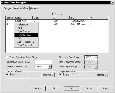
Implementation Panel: This panel lets you decide how to build or implement the filter design. It has several major sections:
Figure 12-2 The Implementation panel
Stage Values: This section lets you specify, stage by stage, the type of circuitry to use and the gain to allocate to each stage. It even lets you edit the poles, Q's, and zeros, by stage. You can swap the pole/Q sets with other stages by clicking in the F0 or Q0 fields with the right mouse button. A pop-up menu lets you select another row to interchange F0/Q sets with. Why would you want to? You may want to optimize signal swing and noise sensitivity. Some circuit implementations can handle larger swings and are less noise sensitive. The zeros are fixed and can't be swapped.
To change the stage, click the left mouse button in the Circuit column at the row where you wish to change the stage. This will display a list of the available circuit implementations for the selected filter type and response. This list will have a maximum of eight circuits, but may have as little as three circuits, since not all circuits types can realize the requisite transfer function.
When the filter circuit is created, the stages are added and numbered from one on the left to N on the right. The input is always on the left and the output or last stage is always on the right.
171
Same Circuit for Each Stage: This option forces all stages to use the same circuit. When disabled, you can specify different circuits for each stage.
Impedance Scale Factor: This option lets you specify a scale factor to apply to all passive component values. The factor multiplies all resistor values and divides all capacitor values. It does not change the shape of the response curve, but shifts component values to more suitable or practical values.
Opamp Model to Use: By default, the model is set to $IDEAL. This model is a voltage controlled current source with a small output resistance. It has a very large gain, infinite bandwidth, and no leakage. Its main purpose is to demonstrate how the filter will behave with a nearly perfect device. You can select a different model from the list. It contains hundreds of popular OPAMP models. Vendor supplied OPAMP subcircuit models are not included in the list.
Resistor Values: This option determines how resistor values are chosen. During the implementation phase, when the circuit is being created, MC7 calculates the exact resistor values required by the design. Of course, resistors precise to 16 digits are impractical, so you must choose whether you want to create the circuit using the exact values, or to use closest fit values chosen from a list of standard parts. The choice is compounded somewhat in that you may be using mostly standard part values, but trimming some. There are several lists of standard parts, and you may add to them or make new lists to special requirements. See the section on list format at the end of this chapter. The Browse button lets you select the file containing the resistor values to use when the Exact check box is disabled.
Capacitor Values: This option lets you decide how the capacitor values will be determined. It works as described in the Resistor Values section.
Odd Low Pass Stage: This option lets you select the last stage to use for low pass filters. There are several different kinds. LODD1 is a simple RC filter. LODD2 is an RC filter, buffered with a non-inverting unity-gain amplifier. LODD3 is an RC filter, buffered with an inverting unity-gain amplifier.
Odd High Pass Stage: This option lets you select the last stage to use for high pass filters. There are three choices. HODD1 is a simple RC filter. HODD2 is an RC filter, buffered with a non-inverting unity-gain amplifier. HODD3 is an RC filter, buffered with an inverting unity-gain amplifier.
Gain Adjust Stage: This option lets you select the stage to use when a gain adjustment is required. There are two choices. NULL adds no stage, which means the gain specification will be ignored. GADJ is a simple inverting amplifier.
172 Chapter 12: Active Filter Designer

Options Panel: This panel lets you set several options. It looks like this:
Figure 12-3 The Options panel
There are several options:
Component Value Format: This option lets you select whether the component values are to be specified in scientific, engineering, or default notation. You can also set the number of digits to use when specifying the value. These choices are mainly cosmetic, but for some very high order filters, increasing the number of digits from the default of 5 may be necessary to get an exactly correct Bode plot.
Polynomial Format: This option lets you select whether the polynomial coefficient values are to be specified in scientific, engineering, or default notation. It works the same way as the component values format. The polynomial values are used to define the transfer functions, LP, HP, BP, and BR. These functions are used in AC analysis to plot the ideal transfer function alongside the actual filter transfer function for comparison.
173
Plot: This option lets you select what to plot. You can select:
•Gain
•Phase
•Group delay
•Separate plots
These options affect several things.
First, it affects the plot displayed when the Plot button in the lower part of the dialog box is clicked. This plot is simply a graph of the ideal complex frequency transfer function. It shows you how the circuit would perform if built from ideal components.
Second, if the Save To / New Circuit option is selected, it changes the AC analysis setup when the circuit is created. It sets up the analysis plot expressions so that you need only select AC analysis and press F2 to see an actual analysis of both the circuit and the ideal transfer function, plotting the variables selected under the Plot option.
Number of Data Points
You can also set the number of data points to be calculated in the plot by editing this field. The internal plot and the AC analysis plot both use fixed log frequency steps rather than auto. This field determines how many data points will be plotted. The default of 500 is usually sufficient, but for very high order filters, you may need to increase the number of points to retain fidelity near steep band edges.
Show Circuit
When checked, this option shows the filter circuit in the background, responding to user changes to specifications.
Save To: This option lets you select where the filter is placed.
•New Circuit: In this option the filter is placed in a new circuit.
•Current Circuit: In this option the filter is placed in the currently selected circuit.
Create: This option lets you select how the filter is created.
• Circuit: In this option the filter is created and placed into either a new circuit or the current circuit.
174 Chapter 12: Active Filter Designer
• Macro: In this option the filter is created as a macro and placed into either a new or current circuit. The macro consists of a number of stages as in the Circuit option, except that they are contained in a macro circuit which is stored on disk. The macro component is entered into a separate component library file called FILTERS.CMP and is available for use by other circuits.
Text: This lets you decide whether to include several optional pieces of text:
•Show Title: This is a self-documenting block of text formed as a title. It identifies the main specifications of the filter.
•Show Polynomials: The polynomial functions that comprise the design are available in a series of .DEFINE statements that can optionally be included with the circuit. This is sometimes handy as a reference. The polynomial function is a symbolic variable and can be plotted versus frequency as a standard against which the actual circuit output can be compared. The names of the polynomials are as follows:
Type |
Symbolic Polynomial Name |
Low Pass |
LP |
High Pass |
HP |
Bandpass |
BP |
Notch |
BR |
Delay |
LP |
Buttons: There are several buttons at the bottom of the dialog box:
Default: This restores default values to all data fields and option buttons.
Plot: This option displays a plot of the selected characteristic(s). These include gain, phase, and/or group delay, depending upon which of these items have been enabled from the Options panel. The plot is a graph of the ideal transfer function for the selected filter. It is not a plot of the actual transfer function that can be achieved with the chosen circuit(s). For that, you must run AC analysis on the completed circuit. If the specification mode is set to Mode 1, the plot includes a design polygon to show the allowed region for the curve, based upon the design specifications.
175
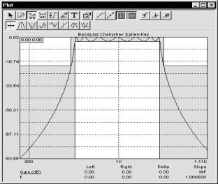
Here is a sample filter plot showing the design polygon.
Figure 12-4 A plot of the filter characteristics
OK: This option builds the circuit to meet the chosen design, using the specified circuits for each stage. If the New Circuit option is enabled, it also sets up the AC analysis dialog box to be ready to plot the circuit output and the theoretical transfer function output over a suitable frequency or time scale. If the specification mode is set to Mode 1, it adds a design polygon to show the allowed region for the curve, based upon the design specifications. After creating the filter circuit, the program exits the dialog box.
Cancel: This option exits the dialog box without saving any changes.
Help: This accesses the Help system.
176 Chapter 12: Active Filter Designer