


10 - 13
|
|
|
|
|
|
|
|
R2 |
|
kT |
CHUNG-YU WU |
V = V |
|
|
|
+ I R = V |
|
+ r |
( |
ln A* + V ) |
|||
|
|
|
|
|
|
||||||
out |
|
BE 3 |
3 2 |
BE 3 |
3 R q |
sg |
|||||
|
|
|
|
|
|
|
|
1 |
|
|
|
2. |
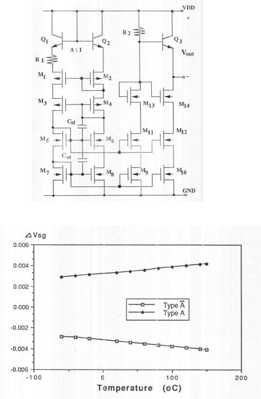
Type |
|
structure |
|
|
|
|
|
|
||
A |
|
|
|
|
|
|
|||||
Cst
3. Type B structure
10 - 14
CHUNG-YU WU
4.Type C structure
The cascode structure of BVR (Type C):
The variation of Vsg versus temperature

10 - 15
CHUNG-YU WU
The simulated output voltages versus temperature in Type A and Type A BVR
The variation of Vsg versus MOS channel length in Type A BVR

10 - 16
CHUNG-YU WU
The Spice simulated output voltages versus temperature in Type C BVR
The measured output voltages versus temperature in the fabricared cascaded-structure BVR(Type C)[ 3.5 ìm CMOS technology , R1=1KÙ(external),R2=25.9KÙ(external)]

10 - 17
CHUNG-YU WU
* Average temperature drift |
|
5.5 ppm/oC |
-60 oC ~ +150 oC |
|
5V~15V |
* |
At 25 oC, average voltage drift 25ìV/V |
||
|
Vout=1.1963V |
~ |
1.1965V |
|
5V |
~ |
15V |
* |
2 mil2 , 0.8 mW at 5V |
|
|
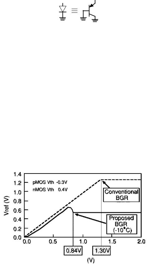
§10-5 CMOS Bandgap Reference with Sub-1-V Operation
Ref.: IEEE JSSC, vol.34, pp.670~674, May 1999
Concept: * Convertional BGR Vref = 1.25V
Can’t be operated below 1V supply. |
|
|
* The built-in voltage |
V f of the diode → |
the current I2b |
The thermal voltage |
Vtherm → the current |
I2a |
(I2a + I 2b )R → Vref |
< 1V |
|
1.Schematic of the proposed BGR
I1 |
I2 |
I3 |
|
||
Vf1 |
I2a |
R2 |
R3 |
||
|
Vf2 |
I2b R4 |
|
I1a |
|
R1 |
|
|
I1b |
|
|
Native NMOS VTHI = −0.2V
NMOS VTHN = +0.7V
PMOS VTHP = −1.0V
10 - 18
CHUNG-YU WU
*The diode is realized by the parasitic P + / n − well / P − substract BJT as
*C1 and C 2 are used to stabilized the circuit.
*The control signal PONRST is used to initialize the BGR circuit when the power
is turned on. |
|
|
|
|
|
||||||||||
* R1 |
= R2 |
|
|
|
|
|
|
|
|
|
|
|
|
||
Va |
= Vb |
|
|
|
|
|
|
|
|
|
|
|
|
||
I1 = I2 |
= I3 and I1a |
= I2a , |
I1b |
= I2b |
|||||||||||
dV f = V f 1 − V f 2 = Vtherm ln(N ) |
, |
N = 100 |
|||||||||||||
I2a |
= |
|
dV f |
|
|
Vtherm |
|
|
|
|
|
||||
|
|
|
|
|
|
|
|
|
|
|
|||||
R3 |
|
|
|
|
|
|
|
||||||||
|
|
|
|
|
|
|
|
|
|
|
|
|
|||
I2b |
= |
V f 1 |
|
V f |
|
|
|
|
|
||||||
|
R2 |
|
|
|
|
|
|||||||||
|
|
|
|
|
|
|
|
|
|
|
|
|
|||
I3 = I 2 = I2a + I2b |
|
|
|
|
|
||||||||||
Vref |
= R4 I3 |
= |
R4 |
V f 1 |
+ |
R4 |
dV f |
|
|
||||||
|
|
|
|
||||||||||||
|
|
|
|
|
|
|
|
|
R2 |
|
R3 |
|
|
||
2. Simulated |
Vref characteristics |
|
|||||||||||||
VDD

10 - 19
CHUNG-YU WU
*Vref |
= 1.25V |
conventional BGR |
*Vref |
= 0.84V |
proposed BGR |
3.Minimum VDD
min V1 @ Vs @ Vb -VTHI @ V f + VTHI @ VDD +VTHP = minVDD - VTHP
Þmin VDD = V f + VTHI + VTHP @ 0.8 ~ 1.0V
0.54-0.2 -0.3
4.Measured results:
VDD
|
|
VDD |
|
|
*TC @ 60 ppm / O C |
27O ~ 125O C |
|
||
Voltage drift (average) |
@ 600μV /V |
2.2V~4V |
||

11-1
CHUNG-YU WU
CH 11 Digital-to-Analog Converters (DACs) in CMOS
Technology
§11-1 Introduction
1. Block diagram
Analog Signal |
|
|
|
Analog |
|
( Video, Audio, |
|
|
|
||
Filtering |
|
D/A |
Output |
||
Sensor.....) |
Digital |
||||
Conversion |
|
||||
|
and A/D |
Processing |
|
||
|
Conversion |
and Filtering |
|
||
|
|
|
|||
|
|
Control |
|
|
|
Analog World |
Digital World |
Analog World |
|||
(Digital signal processing has better noise immunity than analog signal processing.)
Fig. 11.1 A block diagram of a typical signal processing system
Digital |
Data |
|
D/A |
|
|
Output |
|
Analog |
||
Data |
|
Sample |
|
|||||||
Latches |
|
Converter |
|
Output |
||||||
Input |
|
and Hold |
|
|||||||
|
|
|
|
|
|
|
||||
|
|
|
|
|
|
|
|
|
|
|
|
|
|
|
|
|
|
|
|
|
|
Control
Fig. 11.2 Functional block diagram of a D/A converte

11-2
|
|
CHUNG-YU WU |
2. Ideal DAC: |
|
|
Analog output signal Vout = Vref (b 2-1+b |
2-2+ ---- +b 2-N) |
|
1 |
2 |
N |
Vref: analog reference signal
b1 … … . bN : N-bit digital data input
The signal change when one LSB changes is VLSB
VLSB ≡ Vref
2 N
If in LSB unit, 1LSB= 1 2N
3.DAC performance specifications
(1)Resolution: The number of distinct analog levels corresponding to the
different digital words.
N-bit resolution → 2Ndistinct analog levels.
(2) Offset error:
|
|
|
Eoff (DAC) ≡ |
Vout |
|
|
0....0 |
( LSB) |
|
|
|||||||||||||||||||
|
|
|
|
|
|
||||||||||||||||||||||||
(3) Gain error: |
VLSB |
|
|
|
|||||||||||||||||||||||||
|
|
|
|
|
|
|
|
|
|
|
|
|
|
|
|
|
|
|
|
|
|
|
|
||||||
|
|
|
|
|
|
|
|
|
|
|
|
|
|
|
|
|
|
|
|
|
|
|
|
|
|
|
|||
|
|
|
Egain (DAC) ≡ [ |
Vout |
|
1....1 |
− |
Vout |
|
|
0.....0 |
]−(2N −1) (LSB) |
|||||||||||||||||
|
|
|
|
|
|
||||||||||||||||||||||||
|
|
|
|
||||||||||||||||||||||||||
|
|
|
|
VLSB |
|||||||||||||||||||||||||
|
Vout |
|
|
|
VLSB |
|
|
|
|
|
|
|
|
|
|
|
|
||||||||||||
|
|
|
|
|
|
|
|
|
|
|
|
|
|
|
|
|
|
|
|
|
|
|
|
|
|||||
|
|
|
|
|
|
|
|
|
|
|
|
|
|
|
|
|
|
|
|
|
|
|
|||||||
|
|
|
|
|
|
|
|
|
|
|
|
|
|
|
|
|
|
|
|
|
|
|
|
|
|
|
|||
VLSB |
|
Ideal transfer |
|
|
|
|
|
|
|
|
Gain error |
||||||||||||||||||
|
|
|
|
|
|
|
|
|
|||||||||||||||||||||
(LSB) |
|
|
|
|
|
|
|
|
|
||||||||||||||||||||
|
|
response |
|
|
|
|
|
|
|
|
|
|
|||||||||||||||||
|
|
|
|
|
|
|
|
|
|
|
|
|
|
|
|||||||||||||||
|
|
|
|
|
|
|
|
|
|
|
|
|
|
|
|
|
|
|
|
|
|||||||||
|
|
|
|
|
|
|
|
|
|
|
|
|
|
|
|
|
|
|
|
|
|
|
|
|
|
|
|
|
|
|
|
|
|
|
|
|
|
|
|
|
|
|
|
|
|
|
|
|
|
|
|
|
|
|
|
|
|
|
|
|
|
|
|
|
|
|
|
|
|
|
|
|
|
|
|
|
|
|
|
|
|
|
|
|
|
|
|
|
|
|
|
|
|
|
|
|
|
|
|
|
|
|
|
|
|
|
|
|
|
|
|
|
|||||||
|
|
|
|
|
|
|
Actual transfer |
|
|
|
|
|
|
|
|
|
|
|
|
|
|||||||||
|
|
|
|
|
|
|
|
|
|
|
|
|
|
|
|
|
|
|
|
||||||||||
|
|
|
|
|
|
|
response |
|
|
|
|
|
|
|
|
|
|
|
|
|
|||||||||
|
|
|
|
|
|
|
|
|
|
|
|
|
|
|
|
|
|
|
|
||||||||||
|
|
|
|
|
|
|
|
|
|
Actual transfer |
|
response with |
|||||||||||||||||
|
|
|
|
|
|
|
|
|
|
|
|
|
|
||||||||||||||||
|
|
|
|
|
|
|
|
|
|
|
|||||||||||||||||||
|
|
|
|
|
|
|
|
|
|
||||||||||||||||||||
Offset |
|
|
|
|
|
|
|
|
|
|
|
|
|
|
Eoff(DAC) |
set to zero |
|||||||||||||
|
|
|
|
|
|
|
|
|
|
|
|||||||||||||||||||
|
|
o |
|
|
|
|
|
|
|
|
|||||||||||||||||||
error |
|
|
|
|
|
|
|
|
|
|
|
|
|
|
|
|
|
|
|
|
|
|
|
|
|
|
|||
|
|
|
|
|
|
|
|
|
|
|
|
|
|
|
|
|
|
|
|
|
|
|
|
|
|
|
|
||
0......0 |
|
|
|
|
|
|
|
|
|
|
|
1......1 |
Digital Data |
||||||||||||||||
|
|
|
|
|
|
|
|
|
|
|
|
|
|
||||||||||||||||
Input Bin