

Fundamentals of Microelectronics
.pdfBR |
Wiley/Razavi/Fundamentals of Microelectronics [Razavi.cls v. 2006] |
June 30, 2007 at 13:42 |
421 (1) |
|
|
|
|
Sec. 9.1 |
Cascode Stage |
421 |
Solution
Since Q1 and Q2 are identical and biased at the same current level, Eq. (9.7) can be simplified by noting that gm = IC=VT , rO = VA=IC, and r = VT =IC:
|
|
|
|
|
|
VA2 |
|
VT |
|
||||
Rout |
IC1 |
|
VA1 |
|
I |
C2 |
|
I |
C1 |
(9.8) |
|||
VT |
IC1 |
|
|
|
|
||||||||
|
|
|
|
VA2 |
+ |
|
VT |
|
|||||
|
|
|
|
|
|
IC2 |
|
IC1 |
|
||||
|
|
|
|
|
|
|
|
|
|||||
|
1 |
|
VA |
|
|
VAVT |
|
|
; |
(9.9) |
|||
|
|
|
|
|
|
|
|
|
|||||
|
IC1 |
|
VT |
|
VA + VT |
|
|||||||
where IC = IC1 = IC2 and VA = VA1 = VA2. At room temperature, VT 26 mV and hence
Rout 328:9 k : |
(9.10) |
By comparison, the output resistance of Q1 with no degeneration would be equal to rO1 = 5 k ; i.e., “cascoding” has boosted Rout by a factor of 66 here. Note that rO2 and r 1 are comparable in this example.
Exercise
What Early voltage is required for an output resistance of 500 k ?
It is interesting to note that if rO2 becomes much greater than r 1, then Rout1 approaches
Rout;max gm1rO1r 1 |
(9.11) |
1rO1: |
(9.12) |
This is the maximum output impedance provided by a bipolar cascode. After all, even with rO2 = 1 (Fig. 9.3) [or RE = 1 in (9.1)], r 1 still appears from the emitter of Q1 to ac ground, thereby limiting Rout to 1rO1.
R out

 Q 1
Q 1
r π1
 Ideal
Ideal
Figure 9.3 Cascode topology using an ideal current source.
Example 9.2
Suppose in Example 9.1, the Early voltage of Q2 is equal to 50 V.3 Compare the resulting output impedance of the cascode with the upper bound given by Eq. (9.12).
3In integrated circuits, all bipolar transistors fabricated on the same wafer exhibit the same Early voltage. This example applies to discrete implementations.

BR |
Wiley/Razavi/Fundamentals of Microelectronics [Razavi.cls v. 2006] |
June 30, 2007 at 13:42 |
422 (1) |
|
|
|
|
422 Chap. 9 Cascode Stages and Current Mirrors
Solution
Since gm1 = (26 ),1, r 1 = 2:6 k , rO1 = 5 k , and rO2 = 50 k , we have
Rout gm1rO1(rO1jjr 1) |
(9.13) |
475 k : |
(9.14) |
The upper bound is equal to 500 k , about 5% higher.
Exercise
Repeat the above example if the Early voltage of Q1 is 10 V.
Example 9.3
We wish to increase the output resistance of the bipolar cascode of Fig. 9.2(a) by a factor of two through the use of resistive degeneration in the emitter of Q2. Determine the required value of the degeneration resistor if Q1 and Q2 are identical.
Solution
As illustrated in Fig. 9.4, we replace Q2 and RE with their equivalent resistance from (9.1):
Vb1 |
|
|
|
|
|
|
|
R out |
|
|
|
|
|
|
|
R out |
|
|
|
|
|
|
|
|
|
|
|
|
|
|
|||||
|
|
|
|
|
Q 1 |
|
|
|
|
|
|
|
|
||||
|
|
|
|
|
|
|
|
|
|
|
|
|
|
||||
|
|
|
|
|
|
|
|
|
|
|
|||||||
|
|
|
|
|
|
|
|
R outA |
Vb |
|
|
|
|
Q 1 |
|
||
|
|
|
|
|
|
|
|
|
|
|
|
|
|||||
Vb2 |
|
|
|
|
|
Q 2 |
|
|
|
|
|
|
|
RoutA |
|
||
|
|
|
|
|
|
|
|
|
|
|
|
|
|||||
|
|
|
|
|
|
|
|
|
|
|
|
|
|||||
|
|
|
|
|
|
|
|
|
|
|
|
|
|
||||
|
|
|
|
|
|
|
|
|
|||||||||
Figure 9.4 . |
|
|
|
|
|
|
|
RE |
|
|
|
|
|
|
|
|
|
|
|
|
|
|
|
|
|
|
|
|
|
|
|
|
|
||
|
|
|
|
|
|
|
|
|
|
|
|
|
|
|
|
|
|
|
|
|
|
|
|
|
|
|
|
|
|
|
|
|
|
|
|
|
|
|
|
|
|
|
|
|
|
|
|
|
|
|
|
|
|
RoutA = [1 + gm2(REjjr 2)]rO2 + REjjr 2: |
(9.15) |
||||||||||||||||
It follows from (9.7) that |
|
|
|
|
|
|
|
|
|
|
|
|
|
|
|
|
|
|
Rout gm1rO1(RoutAjjr 1): |
|
|
|
|
|
|
(9.16) |
|||||||||
We wish this value to be twice that given by (9.7):
RoutAjjr 1 = 2(rO2jjr 1): |
(9.17) |
||
That is, |
|
|
|
RoutA = |
2rO2r 1 |
: |
(9.18) |
|
|||
|
r 1 , rO2 |
|
|
In practice, r 1 is typically less than rO2, and no positive value of RoutA exists! In other words, it is impossible to double the output impedance of the cascode by emitter degeneration.

BR |
Wiley/Razavi/Fundamentals of Microelectronics [Razavi.cls v. 2006] |
June 30, 2007 at 13:42 |
423 (1) |
|
|
|
|
Sec. 9.1 |
Cascode Stage |
423 |
Exercise
Is there a solution if the output impedance must increase by a factor of 1.5?
What does the above result mean? Comparing the output resistances obtained in Examples 9.1 and 9.2, we recognize that even identical transistors yield an Rout (= 328:9 k ) that is not far from the upper bound (= 500 k ). More specifically, the ratio of (9.7) and (9.12) is equal to rO2=(rO2 + r 1), a value greater than 0.5 if rO2 > r 1.
For completeness, Fig. 9.5 shows a pnp cascode, where Q1 serves as the cascode device and Q2 as the degeneration device. The output impedance is given by (9.5).
VCC
Vb2 
 Q 2
Q 2
Vb1 
 Q 1
Q 1
R out
Figure 9.5 PNP cascode current source.
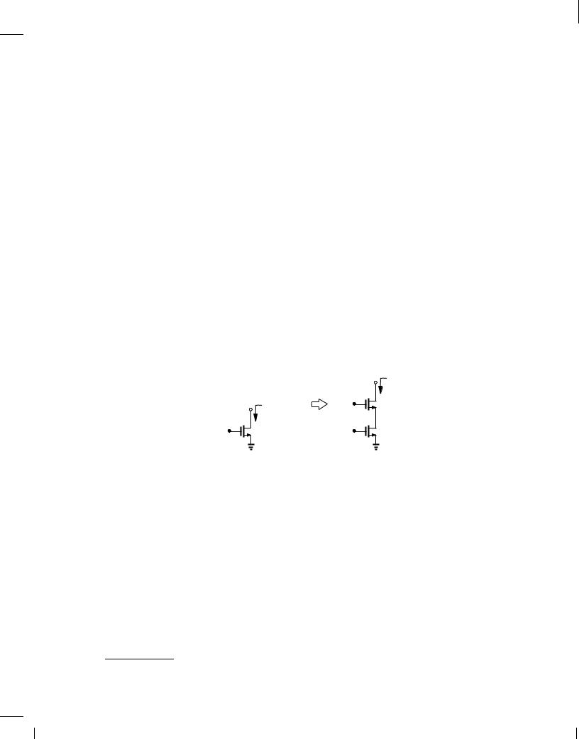
While we have arrived at the cascode as an extreme case of emitter degeneration, it is also possible to view the evolution as illustrated in Fig. 9.6. That is, since Q2 provides only an output impedance of rO2, we “stack” Q1 on top of it to raise Rout.
R out  g m1 r O1 ( r O2
 r π1 )
|
R out = r O2 |
Vb1 |
Q 1 |
Vb2 |
Q 2 |
Vb2 |
Q 2 |
Figure 9.6 Evolution of cascode topology viewed as stacking Q1 atop Q2.
Example 9.4
Explain why the topologies depicted in Fig. 9.7 are not cascodes.
|
|
|
R out |
|
R out |
|
VCC |
|
VCC |
|
||
Vb1 |
Q |
|
Vb1 |
Q |
|
|
Vb1 |
Q 2 |
|
g |
1 |
r O2 |
1 |
1 |
|
|
X |
|
m2 |
||||||
|
|
|
|
|||||||||
|
X |
|
|
|
1 |
r O2 |
Vb2 |
Q 1 |
Vb2 |
Q 1 |
|
|
Vb2 |
|
|
|
g m2 |
|
|
||||||
Q 2 |
|
|
|
|
|
|
|
|
|
|||
|
|
|
|
|
|
|
|
|
|
|||
|
|
|
|
|
|
|
|
R out |
|
|
R out |
|
|
|
|
(a) |
|
|
|
|
|
(b) |
|
|
|
Figure 9.7

BR |
Wiley/Razavi/Fundamentals of Microelectronics [Razavi.cls v. 2006] |
June 30, 2007 at 13:42 |
424 (1) |
|
|
|
|
424 |
Chap. 9 |
Cascode Stages and Current Mirrors |
Solution
Unlike the cascode of Fig. 9.2(a), the circuits of Fig. 9.7 connect the emitter of Q1 to the emitter of Q2. Transistor Q2 now operates as a diode-connected device (rather than a current source), thereby presenting an impedance of (1=gm2)jjrO2 (rather than rO2) at node X. Given by (9.1), the output impedance, Rout, is therefore considerably lower:
R |
|
= 1 + g |
|
1 |
jjr |
|
jjr |
|
r |
|
+ |
1 |
jjr |
jjr |
|
: |
|
|
|
|
|
|
|
||||||||||
|
out |
m1 |
|
gm2 |
O2 |
|
1 |
|
O1 |
|
gm2 |
O2 |
|
1 |
|
|
In fact, since 1=gm2 rO2, r 1 and since gm1 gm2 (why?),
R |
|
1 + gm1 |
r |
+ |
1 |
out |
|
||||
|
gm2 |
O1 |
|
gm2 |
|
|
|
|
|
||
|
|
2rO1: |
|
|
|
The same observations apply to the topology of Fig. 9.7(b).
Exercise
Estimate the output impedance for a collector bias current of 1 mA and VA = 8 V.
(9.19)
(9.20)
(9.21)
MOS Cascodes The similarity of Eqs. (9.1) and (9.3) for degenerated stages suggests that cascoding can also be realized with MOSFETs so as to increase the output impedance of a current source. Illustrated in Fig. 9.8, the idea is to replace the degeneration resistor with a MOS current
|
R out |
|
R out |
|
|
|
|
Vb1 |
M 1 |
Vb |
M 1 |
|
X |
||
|
|
r O2 |
|
Vb2 |
M 2 |
|
|
|
|
Figure 9.8 MOS cascode current source and its equivalent.
source, thus presenting a small-signal resistance of rO2 from X now be written as
Rout = (1 + gm1rO2)rO1 + rO2
gm1rO1rO2;
to ground. Equation (9.3) can
(9.22)
(9.23)
where it is assumed gm1rO1rO2 rO1, rO2.
Equation (9.23) is an extremely important result, implying that the output impedance is proportional to the intrinsic gain of the cascode device.
Example 9.5
Design an NMOS cascode for an output impedance of 500 k and a current of 0.5 mA. For simplicity, assume M1 and M2 in Fig. 9.8 are identical (they need not be). Assume nCox = 100 A=V2 and = 0:1 V,1.
BR |
Wiley/Razavi/Fundamentals of Microelectronics [Razavi.cls v. 2006] |
June 30, 2007 at 13:42 |
425 (1) |
|
|
|
|
Sec. 9.1 Cascode Stage 425
Solution
We must determine W=L for both transistors such that
gm1rO1rO2 = 500 k : |
(9.24) |
|||||
Since rO1 = rO2 = ( ID),1 = 20 k , we require that gm1 = (800 ),1 and hence |
|
|||||
|
|
|
|
|
|
|
r2 nCox W ID = |
1 |
|
: |
(9.25) |
||
800 |
|
|||||
|
L |
|
|
|||
It follows that |
|
|
|
|
||
|
W = 15:6: |
|
|
|
(9.26) |
|
|
L |
|
|
|
|
|
We should also note that gm1rO1 = 25 1.
Exercise
What is the output resistance if W=L = 32?
Invoking the alternative view depicted in Fig. 9.6 for the MOS counterpart (Fig. 9.9), we
R out  g m1 r O1 r O2
|
R out = r O2 |
Vb1 |
M 1 |
|
|
|
X |
Vb2 |
M 2 |
Vb2 |
M 2 |
Figure 9.9 MOS cascode viewed as stack of M1 atop of M2.
recognize that stacking a MOSFET on top of a current source “boosts” the impedance by a factor of gm2rO2 (the intrinsic gain of the cascode transistor). This observation reveals an interesting point of contrast between bipolar and MOS cascodes: in the former, raising rO2 eventually leads to Rout;bip = rO1, whereas in the latter, Rout;MOS = gm1rO1rO2 increases with no bound.4 This is because in MOS devices, and r are infinite (at low frequencies).
Figure 9.10 illustrates a PMOS cascode. The output resistance is given by (9.22).
Example 9.6
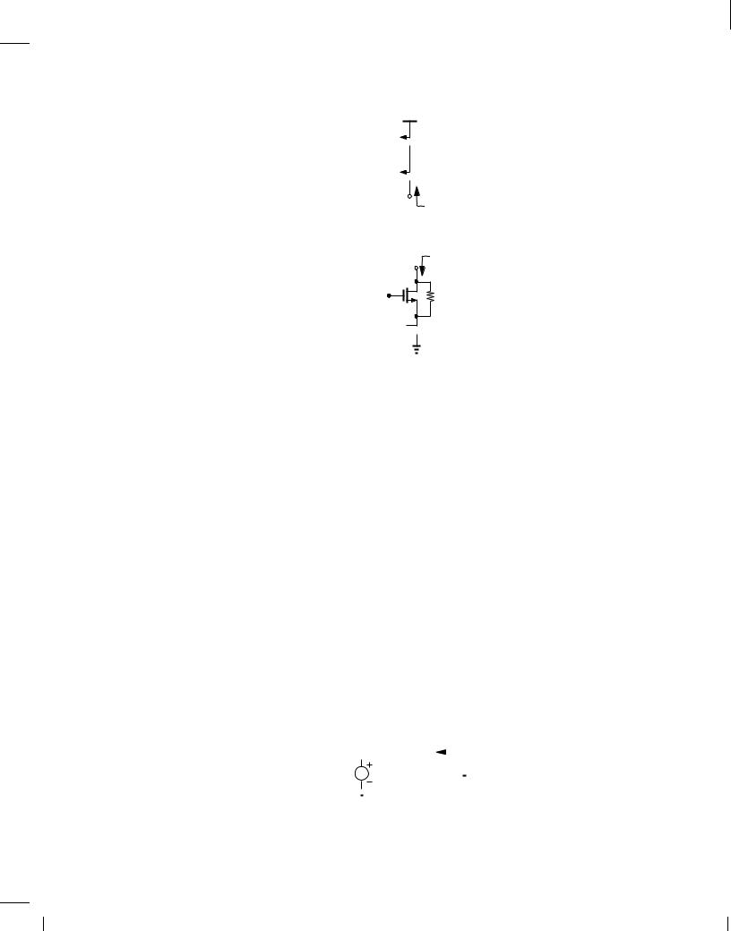
During manufacturing, a large parasitic resistor, Rp, has appeared in a cascode as shown in Fig. 9.11. Determine the output resistance.
Solution
We observe that Rp is in parallel with rO1. It is therefore possible to rewrite (9.23) as
Rout = gm1(rO1jjRp)rO2: |
(9.27) |
4In reality, other second-order effects limit the output impedance of MOS cascodes.
BR |
Wiley/Razavi/Fundamentals of Microelectronics [Razavi.cls v. 2006] |
June 30, 2007 at 13:42 |
426 (1) |
|
|
|
|
426 |
Chap. 9 |
Cascode Stages and Current Mirrors |
VDD
Vb2 

 M 2
M 2
X
Vb1 

 M 1
M 1
R out
Figure 9.10 PMOS cascode current source.
|
R out |
|
M 1 |
Vb1 |
RP |
Vb2 

 M 2
M 2
Figure 9.11
If gm1(rO1jjRp) is not much greater than unity, we return to the original equation, (9.22), substituting rO1jjRp for rO1:
Rout = (1 + gm1rO2)(rO1jjRp) + rO2: |
(9.28) |
Exercise
What value of Rp degrades the output impedance by a factor of two?
9.1.2 Cascode as an Amplifier
In addition to providing a high output impedance as a current source, the cascode topology can also serve as a high-gain amplifier. In fact, the output impedance and the gain of amplifiers are closely related.
For our study below, we need to understand the concept of the transconductance for circuits. In Chapters 4 and 6, we defined the transconductance of a transistor as the change in the collector or drain current divided by the change in the base-emitter or gate-source voltage. This concept can be generalized to circuits as well. As illustrated in Fig. 9.12, the output voltage is set to zero
|
|
|
|
|
|
Circuit |
i out |
|||||
v in |
|
|
|
|
|
|
|
|||||
|
|
|
|
|
|
|
|
|
|
|
ac |
|
|
|
|
|
|
|
|
|
|
|
|
||
|
|
|
|
|
|
|
|
|
|
|
GND |
|
|
|
|
|
|
|
|
|
|
|
|
||
|
|
|
|
|
|
|
|
|
|
|
|
|
Figure 9.12 Computation of transconductance for a circuit.
be shorting the output node to ground, and the “short-circuit transconductance” of the circuit is

BR |
Wiley/Razavi/Fundamentals of Microelectronics [Razavi.cls v. 2006] |
June 30, 2007 at 13:42 |
427 (1) |
|
|
|
|
Sec. 9.1 Cascode Stage 427
defined as
Gm = |
iout |
jvout=0: |
(9.29) |
|
|||
|
vin |
|
|
The transconductance signifies the “strength” of a circuit in converting the input voltage to a current.5 Note the direction of iout in Fig. 9.12.
Example 9.7
Calculate the transconductance of the CS stage shown in Fig. 9.13(a).
|
|
VDD |
|
|
|
VDD |
|
|
R D |
|
|
R D |
|
i out |
|
|
|
v out |
|
|
|
|
|
|
|
|
|
|
|
ac |
|
v in |
M |
|
v in |
|
M |
|
|
1 |
|
1 |
GND |
||||
|
|
|
|
|
|||
|
(a) |
|
|
|
(b) |
|
|
Figure 9.13
Solution
As depicted in Fig. 9.13(b), we short the output node to ac ground and, noting that RD no current (why?), write
Gm = iout vin
= iD1
vGS1
carries
(9.30)
(9.31)
= gm1: |
(9.32) |
Thus, in this case, the transconductance of the circuit is equal to that of the transistor.
Exercise
How does Gm change if the width and bias current of the transistor are doubles?
Lemma The voltage gain of a linear circuit can be expressed as
Av = ,GmRout; |
(9.33) |
where Rout denotes the output resistance of the circuit (with the input voltage set to zero). Proof We know that a linear circuit can be replaced with its Norton equivalent [Fig. 9.14(a)]. Norton's theorem states that iout is obtained by shorting the output to ground (vout = 0) and
5While omitted for simplicity in Chapters 4 and 6, the condition vout = 0 is also required for the transconductance of transistors. That is, the collector or drain must by shorted to ac ground.

BR |
Wiley/Razavi/Fundamentals of Microelectronics [Razavi.cls v. 2006] |
June 30, 2007 at 13:42 |
428 (1) |
|
|
|
|
428 |
Chap. 9 |
Cascode Stages and Current Mirrors |
|
Vout |
|
|
Vout |
v in |
|
i out |
Rout |
(a)
i out
v in
(b)
Figure 9.14 (a) Norton equivalent of a circuit, (b) computation of short-circuit output current .
computing the short-circuit current [Fig. 9.14(b)]. We also relate iout to vin by the transconductance of the circuit, Gm = iout=vin. Thus, in Fig. 9.14(a),
|
|
|
|
|
|
|
|
|
|
|
|
vout = ,ioutRout |
|
|
|
|
|
|
|
|
|
|
|
|
|
|
|
(9.34) |
||||||||||||||||
|
|
|
|
|
|
|
|
|
|
|
|
|
|
= ,GmvinRout |
|
|
|
|
|
|
|
|
(9.35) |
|||||||||||||||||||||
and hence |
|
|
|
|
|
|
|
|
|
|
|
|
|
|
|
|
|
|
|
|
|
|
|
|
|
|
|
|
|
|
|
|
|
|
|
|
|
|
|
|
|
|
|
|
|
|
|
|
|
|
|
|
|
|
|
|
vout = ,GmRout: |
|
|
|
|
|
|
|
|
|
|
|
|
|
|
|
(9.36) |
||||||||||||||||
|
|
|
|
|
|
|
|
|
|
|
|
vin |
|
|
|
|
|
|
|
|
|
|
|
|
|
|
|
|
|
|
|
|
|
|
|
|
|
|
|
|
|
|
|
|
Example 9.8 |
|
|
|
|
|
|
|
|
|
|
|
|
|
|
|
|
|
|
|
|
|
|
|
|
|
|
|
|
|
|
|
|
|
|
|
|||||||||
Determine the voltage gain of the common-emitter stage shown in Fig. 9.15(a). |
|
|
|
|
|
|
|
|
|
|
|
|||||||||||||||||||||||||||||||||
|
|
|
|
|
|
|
|
|
|
VCC |
|
|
|
|
|
|
|
|
|
|
|
|
|
|
|
|
|
|
|
|
|
|
|
|
|
|
i X |
|
|
|
||||
|
|
|
|
|
|
|
|
|
|
|
|
|
|
|
|
|
|
|
|
|
|
|
|
|
|
|
|
|
|
|
|
|
|
|
|
|
|
|
||||||
|
|
|
|
|
|
|
|
|
|
I 1 |
|
|
|
|
|
|
|
|
|
i out |
|
|
|
|
|
|
|
|
|
|
|
|
|
|
||||||||||
v in |
|
|
|
|
|
|
|
|
|
|
v out |
v in |
|
|
|
|
|
|
|
|
ac |
|
|
|
|
|
|
|
|
|
|
|
|
|
v X |
|||||||||
|
|
|
|
|
Q |
|
|
|
|
|
|
Q |
|
|
|
|
|
|
|
|
|
Q |
|
|
|
|
|
|
|
|||||||||||||||
|
|
|
|
|
|
|
|
|
|
|
|
|
|
|
|
|
|
|
|
|
|
|
|
|
|
|||||||||||||||||||
|
|
|
|
|
1 |
|
|
|
|
|
|
1 |
|
|
|
|
|
GND |
|
|
|
|
|
1 |
|
|
|
|
|
|||||||||||||||
|
|
|
|
|
|
|
|
|
|
|
|
|
|
|
|
|
|
|
|
|
|
|
|
|
|
|
|
|
|
|
|
|
|
|
|
|
|
|
|
|
|
|
|
|
|
|
|
|
|
|
|
|
|
|
|
|
|
|
|
|
|
|
|
|
|
|
|
|
|
|
|
|
|
|
|
|
|
|
|
|
|
|
|
|
|
|
|
|
|
|
|
|
|
|
|
|
|
|
|
|
|
|
|
|
|
|
|
|
|
|
|
|
|
|
|
|
|
|
|
|
|
|
|
|
|
|
|
|
|
|
||||
|
|
(a) |
|
|
|
|
|
|
|
|
(b) |
|
|
|
|
|
|
|
|
|
(c) |
|
|
|
||||||||||||||||||||
Figure 9.15
Solution
To calculate the short-circuit transconductance of the circuit, we place an ac short from the output to ground and find the current through it [Fig. 9.15(b)]. In this case, iout is simply equal to the collector current of Q1, gm1vin, i.e.,
Gm = iout |
(9.37) |
vin |
|
= gm1: |
(9.38) |

BR |
Wiley/Razavi/Fundamentals of Microelectronics [Razavi.cls v. 2006] |
June 30, 2007 at 13:42 |
429 (1) |
|
|
|
|
Sec. 9.1 |
Cascode Stage |
429 |
Note that rO does not carry a current in this test (why?). Next, we obtain the output resistance as depicted in Fig. 9.15(c):
Rout = vX |
(9.39) |
iX |
|
= rO1: |
(9.40) |
It follows that |
|
Av = ,GmRout |
(9.41) |
= ,gm1rO1: |
(9.42) |
Exercise
Suppose the transistor is degenerated by an emitter resistor equal to RE. The transconductance falls but the ouput resistance rises. Does the voltage gain increase or decrease?
The above lemma serves as an alternative method of gain calculation. It also indicates that the voltage gain of a circuit can be increased by raising the output impedance, as in cascodes.
Bipolar Cascode Amplifier Recall from Chapter 4 that to maximize the voltage gain of a common-emitter stage, the collector load impedance must be maximized. In the limit, an ideal current source serving as the load [Fig. 9.16(a)] yields a voltage gain of
|
|
|
|
VCC |
|
VCC |
|
|
I 1 |
|
|
|
v out |
|
I 1 |
g m1v in |
|
Vb1 |
Q 2 |
|
|
|
v out |
|
v in |
Q 1 |
r O1 |
v in |
Q 1 |
|
||||
|
(a) |
|
|
(b) |
Figure 9.16 (a) Flow of output current generated by a CE stage through rO1, (b) use of cascode to increase the output impedance.
Av = ,gm1rO1 |
(9.43) |
= ,VA : |
(9.44) |
VT |
|
In this case, the small-signal current, gm1vin, produced by Q1 flows through |
rO1, thus generating |
an output voltage equal to ,gm1vinrO1. |
|
Now, suppose we stack a transistor on top of Q1 as shown in Fig. 9.16(b). We know from Section 9.1.1 that the circuit achieves a high output impedance and, from the above lemma, a voltage gain higher than that of a CE stage.

BR |
Wiley/Razavi/Fundamentals of Microelectronics [Razavi.cls v. 2006] |
June 30, 2007 at 13:42 |
430 (1) |
|
|
|
|
430 |
Chap. 9 |
Cascode Stages and Current Mirrors |
Let us determine the voltage gain of the bipolar cascode with the aid of the above lemma. As shown in Fig. 9.17(a), the short-circuit transconductance is equal to iout=vin. As a common-
i out |
|
i out |
|
|||
Q 2 |
|
ac |
|
Q 2 |
|
ac |
|
|
GND |
|
r O2 |
|
GND |
|
|
|
|
X |
|
|
Q 1 |
|
v in |
|
Q 1 |
v in |
|
g |
m1 |
v in |
g |
r O1 |
||
v in |
|
m1 |
|
|||
(a)
(b)
Figure 9.17 (a) Short-circuit output current of a cascode, (b) detailed view of (a).
emitter stage, Q1 still produces a collector current of gm1vin, which subsequently flows through Q2 and hence through the output short:
iout = gm1vin: |
(9.45) |
That is, |
|
Gm = gm1: |
(9.46) |
The reader may view (9.46) dubiously. After all, as shown in Fig. 9.17(b), the collector current of Q1 must split between rO1 and the impedance seen looking into the emitter of Q2. We must therefore verify that only a negligible fraction of gm1vin is “lost” in rO1. Since the base and collector voltages of Q2 are equal, this transistor can be viewed as a diode-connected device having an impedance of (1=gm2)jjrO2. Dividing gm1vin between this impedance and rO1, we have
i |
out |
= g |
v |
|
rO1jjr 2 |
: |
(9.47) |
||
|
m1 |
|
in |
1 |
|
|
|
||
|
|
|
|
|
rO1jjr 2 + |
jjrO2 |
|
|
|
|
|
|
|
|
gm2 |
|
|
||
For typical transistors, 1=gm2 rO2, rO1, and hence |
|
|
|
|
|||||
|
|
iout gm1vin: |
|
|
|
(9.48) |
|||
That is, the approximation Gm = gm1 is reasonable. |
|
|
|
|
|||||
To obtain the overall voltage gain, we write from (9.33) and (9.5), |
|
||||||||
Av = ,GmRout |
|
|
|
|
|
|
(9.49) |
||
= ,gm1 f[1 + gm2(rO1jjr 2)]rO2 + rO1jjr 2g |
(9.50) |
||||||||
,gm1[gm2(rO1jjr 2)rO2 + rO1jjr 2]: |
(9.51) |
||||||||
Also, since Q1 and Q2 carry approximately equal bias currents, gm1 gm2 and rO1 rO2:
Av = ,gm1rO1[gm1(rO1jjr 2) + 1] |
(9.52) |
,gm1rO1gm1(rO1jjr 2): |
(9.53) |