

Fundamentals of Microelectronics
.pdfBR |
Wiley/Razavi/Fundamentals of Microelectronics [Razavi.cls v. 2006] |
June 30, 2007 at 13:42 |
351 (1) |
|
|
|
|
Sec. 7.5 Summary and Additional Examples |
|
|
351 |
||
|
VDD |
|
VDD |
||
|
R G |
|
R G |
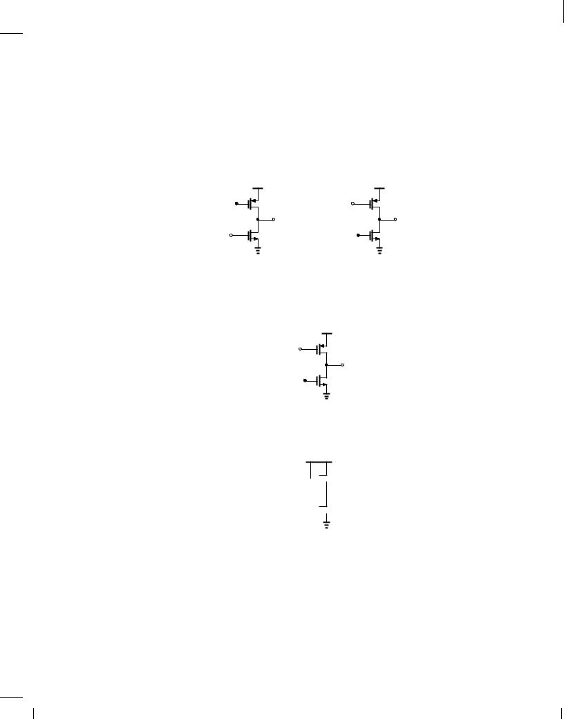
|
|
|
C1 |
|
C1 |
|
|
Vin |
M 1 |
C2 |
Vin |
M 1 |
C2 |
|
|
Vout |
|
|
Vout |
|
|
|
Vb |
M 2 |
|
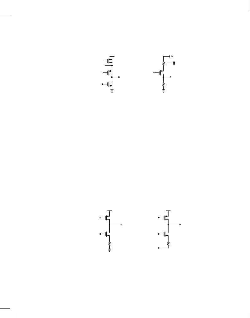
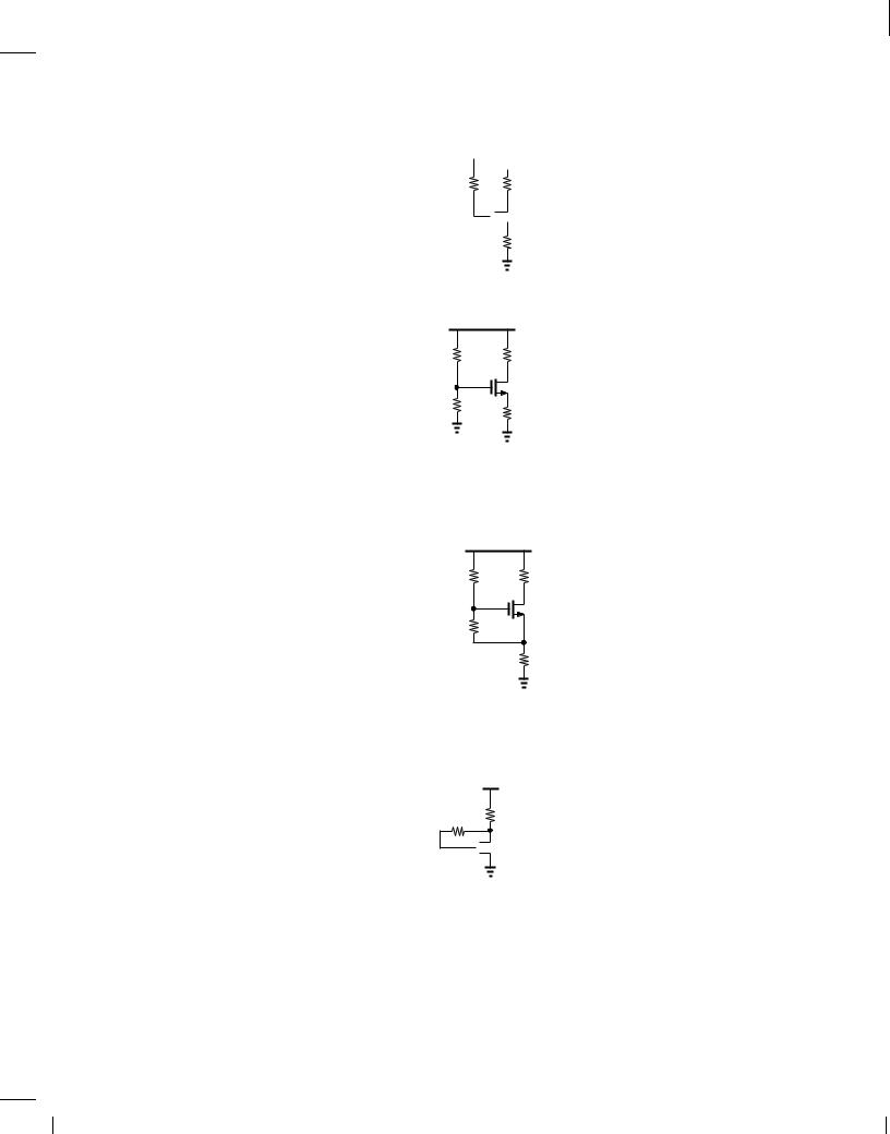
Figure 7.33 Source follower with biasing.
schemes are also similar, with the quadratic ID-VGS relationship supplanting the exponential IC-VBE characteristic.
In this section, we consider a number of additional examples to solidify the concepts introduced in this chapter, emphasizing analysis by inspection.
Example 7.19
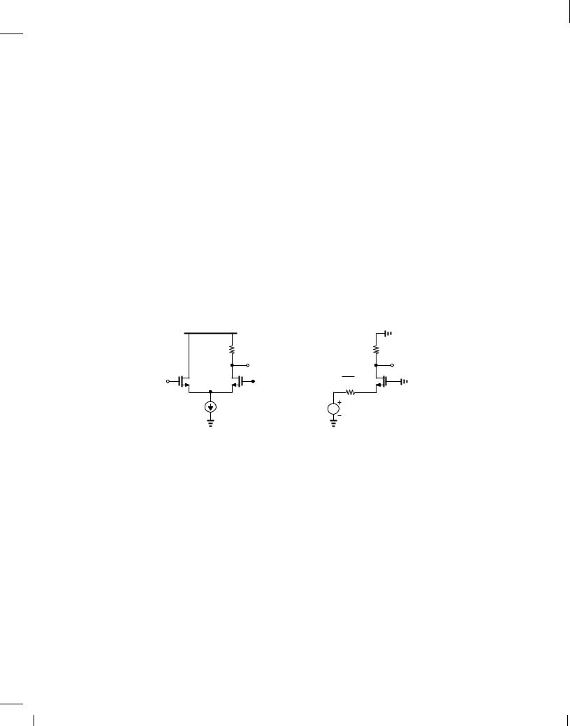
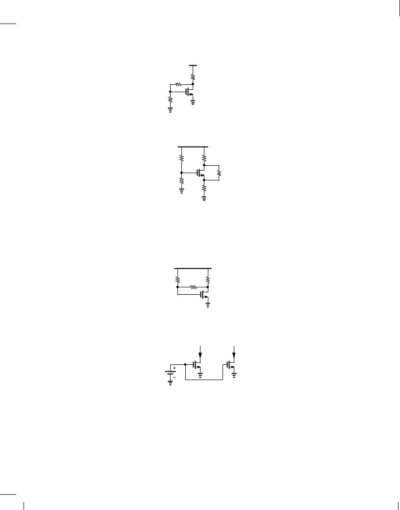
Calculate the voltage gain and output impedance of the circuit shown in Fig. 7.34(a).
|
VDD |
|
|
Vin |
M 1 |
v in |
r O1 |
|
|
Vout |
M 1 |
|
|
v out |
|
|
|
|
Vb |
M 2 |
M 3 |
r O2 |
1 |
r O3 |
|
g m3 |
||||||
|
|
|
|
|
||
|
(a) |
|
|
(b) |
|
Figure 7.34 (a) Example of CS stage, (b) simplified circuit.
Solution
We identify M1 as a common-source device because it senses the input at its gate and generates the output at its drain. Transistors M2 and M3 therefore act as the load, with the former serving as a current source and the latter as a diode-connected device. Thus, M2 can be replaced with a small-signal resistance equal to rO2, and M3 with another equal to (1=gm3)jjrO3. The circuit now reduces to that depicted in Fig. 7.34(b), yielding
A |
|
= ,g |
( |
1 |
jjr |
|
jjr |
|
jjr |
) |
(7.153) |
||
|
|
|
|
|
|||||||||
|
v |
m1 |
|
gm3 |
O1 |
|
O2 |
O3 |
|
|
|||
and |
|
|
|
|
|
|
|
|
|
|
|
|
|
|
Rout = |
|
1 |
jjrO1jjrO2jjrO3: |
|
(7.154) |
|||||||
|
|
|
|
||||||||||
|
|
|
gm3 |
|
|
|
|
|
|
||||
Note that 1=gm3 is dominant in both expressions.
Exercise
Repeat the above example if M2 is converted to a diode-connected device.
BR |
Wiley/Razavi/Fundamentals of Microelectronics [Razavi.cls v. 2006] |
June 30, 2007 at 13:42 |
352 (1) |
|
|
|
|
352 |
Chap. 7 CMOS Amplifiers |
Example 7.20
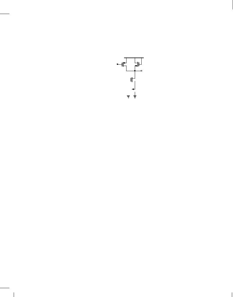
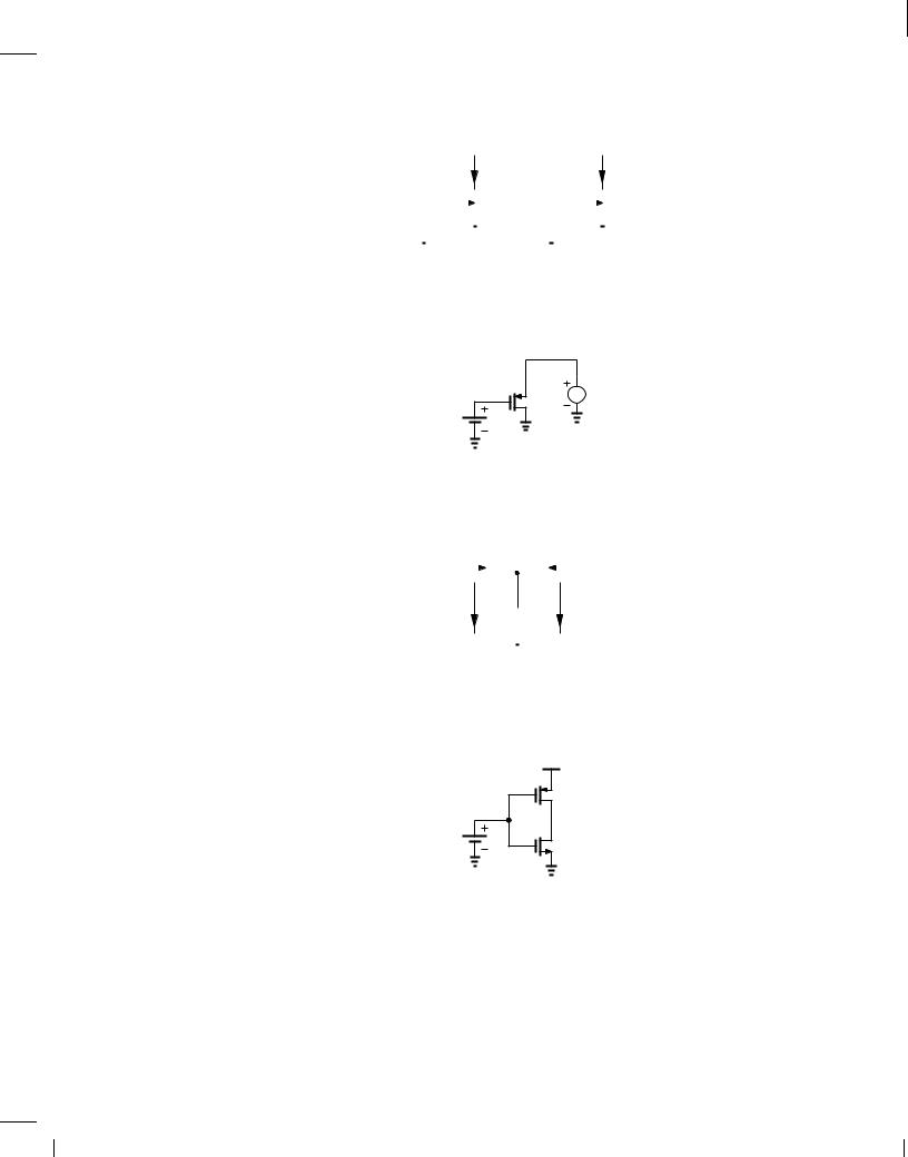
Compute the voltage gain of the circuit shown in Fig. 7.35(a). Neglect channel-length modulation
in M1.
VDD
|
M 3 |
|
1 |
r O3 |
|
|
|
g m3 |
|
Vin |
M 1 |
Vin |
M 1 |
|
|
Vout |
|
|
Vout |
Vb |
M 2 |
|
r O2 |
|
|
(a) |
|
(b) |
|
Figure 7.35 (a) Example of CS stage, (b) simplified circuit.
Solution
Operating as a CS stage and degenerated by the diode-connected device M3, transistor M1 drives the current-source load, M2. Simplifying the amplifier to that in Fig. 7.35(b), we have
Av = , |
|
|
rO2 |
: |
(7.155) |
||
1 |
1 |
|
|||||
|
|
|
+ |
|
jjrO3 |
|
|
|
|
gm1 |
gm3 |
|
|
||
Exercise
Repeat the above example if the gate of M3 is tied to a constant voltage.
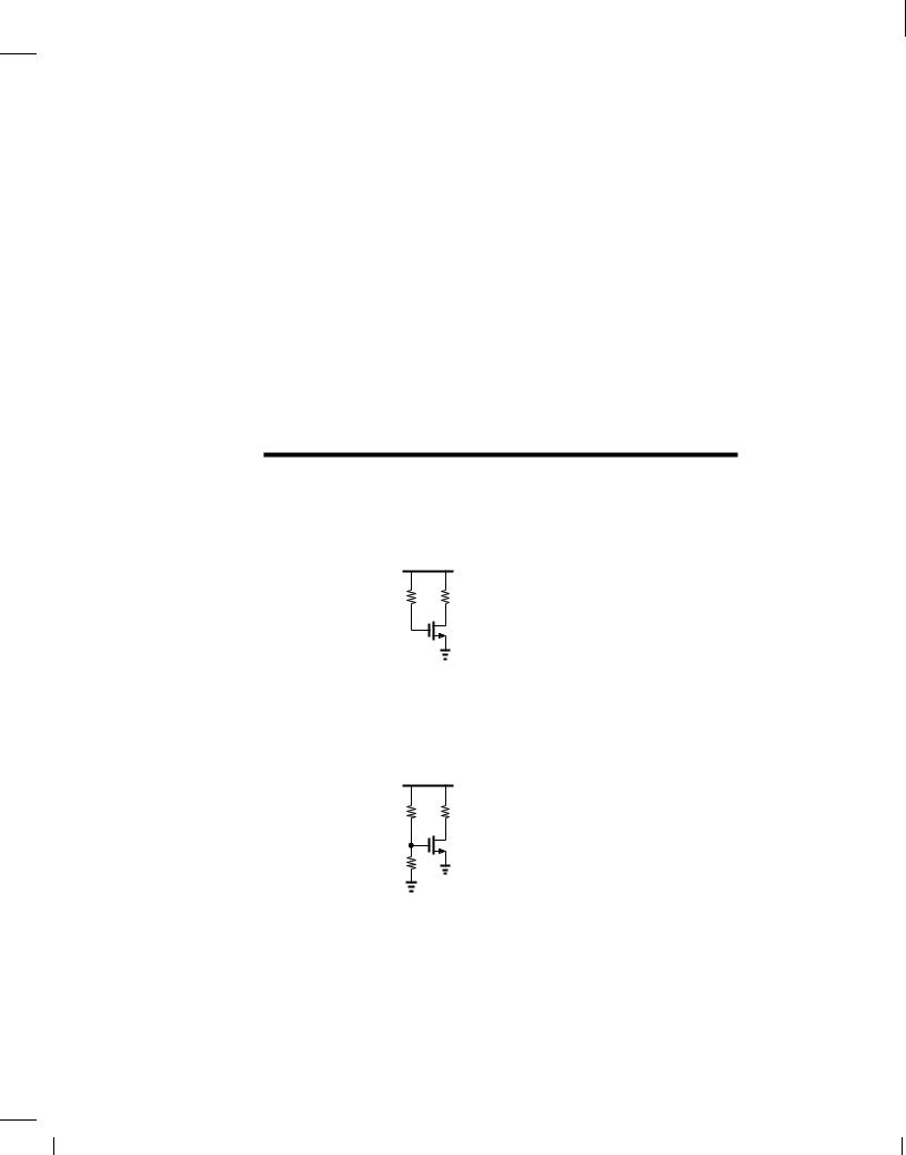
Example 7.21
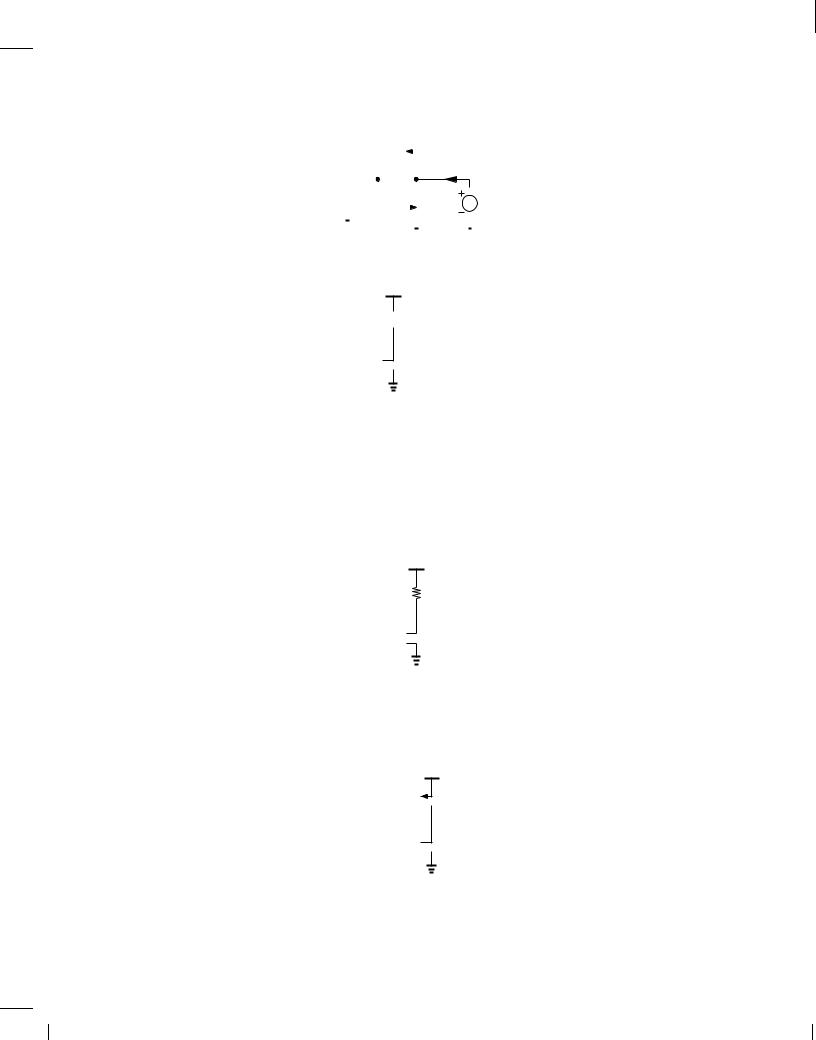
Determine the voltage gain of the amplifiers illustrated in Fig. 7.36. For simplicity, assume rO1 = 1 in Fig. 7.36(b).
|
VDD |
|
VDD |
Vin |
M 2 |
Vb2 |
M 2 |
|
Vout |
|
Vout |
Vb |
M 1 |
Vb1 |
M 1 |
|
RS |
Vin |
RS |
|
|
|
(b)
(a)
Figure 7.36 Examples of (a) CS and (b) CG stages .
Solution
Degenerated by RS, transistor M1 in Fig. 7.36(a) presents an impedance of (1 + gm1rO1)RS + rO1 to the drain of M2. Thus the total impedance seen at the drain is equal to [(1+ gm1rO1)RS +
BR |
Wiley/Razavi/Fundamentals of Microelectronics [Razavi.cls v. 2006] |
June 30, 2007 at 13:42 |
353 (1) |
|
|
|
|
Sec. 7.5 Summary and Additional Examples |
|
|
|
353 |
||
rO1]jjrO2, giving a voltage gain of |
|
|
|
|
|
|
Av = ,gm2 f[(1 + gm1rO1)RS + rO1]jjrO1g: |
(7.156) |
|||||
In Fig. 7.36(b), M1 operates as a common-gate stage and M2 as the load, obtaining (7.109): |
||||||
Av2 = |
|
|
rO2 |
: |
(7.157) |
|
1 |
|
+ RS |
||||
|
|
|
|
|
|
|
|
|
gm1 |
|
|
||
Exercise
Replace RS wit a diode-connected device and repeat the analysis.
Example 7.22
Calculate the voltage gain of the circuit shown in Fig. 7.37(a) if = 0.
|
|
VDD |
|
|
|
RD |
RD |
|
|
Vout |
v out |
Vin |
|
|
1 |
M 1 M 2 |
Vb |
g m1 M 2 |
|
|
I 1 |
|
v in |
|
(a) |
|
(b) |
Figure 7.37 (a) Example of a composite stage, (b) simplified circuit.
Solution
In this circuit, M1 operates as a source follower and M2 as a CG stage (why?). A simple method of analyzing the circuit is to replace vin and M1 with a Thevenin equivalent. From Fig. 7.29(b), we derive the model depicted in Fig. 7.37(b). Thus,
Av = |
|
|
RD |
|
|
: |
(7.158) |
|
|
|
|
|
|||
1 |
+ |
1 |
|
||||
|
|
|
|
|
|
|
|
|
|
gm1 |
gm2 |
|
|
||
|
|
|
|
|
|||
Exercise
What happens if a resistance of value R1 is placed in series with the drain of M1?
BR |
Wiley/Razavi/Fundamentals of Microelectronics [Razavi.cls v. 2006] |
June 30, 2007 at 13:42 |
354 (1) |
|
|
|
|
354 |
Chap. 7 CMOS Amplifiers |
Example 7.23
The circuit of Fig. 7.38 produces two outputs. Calculate the voltage gain from the input to Y and to X. Assume = 0 for M1.
VDD
Vb |
M 3 |
M 4
Vout2
Y
Vin
 M 1
M 1
X 
 Vout1
Vout1


 M 2
M 2
Figure 7.38 Example of composite stage.
Solution
For Vout1, the circuit serves as a source follower. The reader can show that if rO1 = 1, then M3 and M4 do not affect the source follower operation. Exhibiting a small-signal impedance of (1=gm2)jjrO2, transistor M2 acts as a load for the follower, yielding from (7.131)
|
|
1 |
jjrO2 |
|
|
||||||
vout1 |
|
|
|
|
|
|
|
||||
= |
|
|
gm2 |
: |
(7.159) |
||||||
vin |
1 |
|
|
|
1 |
|
|||||
|
|
|
|
|
|
|
|||||
|
|
|
gm2 |
jjrO2 |
+ |
gm1 |
|
|
|
||
For Vout2, M1 operates as a degenerated CS stage with a drain load consisting of the diode-connected device M3 and the current source M4. This load impedance is equal to (1=gm3)jjrO3jjrO4, resulting in
|
|
1 |
|
jjrO3jjrO4 |
|
|
||||
vout2 |
|
|
|
|
|
|
||||
= , |
|
|
gm3 |
: |
(7.160) |
|||||
vin |
1 |
1 |
|
|||||||
|
|
|
|
|||||||
|
|
|
gm1 |
+ |
gm2 |
jjrO2 |
|
|
||
Exercise
Which one of the two gains is higher? Explain intuitively why.
7.6 Chapter Summary
The impedances seen looking into the gate, drain, and source of a MOSFET are equal to infinity, rO (with source grounded), and 1=gm (with gate grounded), respectively .
In order to obtain the required small-signal MOS parameters such as gm and rO, the transistor must be “biased,” i.e., carry a certain drain current and sustain certain gate-source and drain-source voltages. Signals simply perturb these conditions.
BR |
Wiley/Razavi/Fundamentals of Microelectronics [Razavi.cls v. 2006] |
June 30, 2007 at 13:42 |
355 (1) |
|
|
|
|
Sec. 7.6 |
Chapter Summary |
355 |
Biasing techniques establish the required gate voltage by means of a resistive path to the supply rails or the output node (self-biasing).
With a single transistor, only three amplifier topologies are possible: common-source and common-gate stages and source followers.
The CS stage provides a moderate voltage gain, a high input impedance, and a moderate output impedance.
Source degeneration improves the linearity but lowers the voltage gain.
Source degeneration raises the output impedance of CS stages considerably.
The CG stage provides a moderate voltage gain, a low input impedance, and a moderate output impedance.
The voltage gain expressions for CS and CG stages are similar but for a sign.
The source follower provides a voltage gain less than unity, a high input impedance, and a low output impedance, serving as a good voltage buffer.
Problems
In the following problems, unless otherwise stated, assume nCox = 200 A=V2,
pCox = 100 A=V2, = 0, and VTH = 0:4 V for NMOS devices and ,0:4 V for PMOS devices.
1. In the circuit of Fig. 7.39, determine the maximum allowable value of W=L if M1 must
|
VDD = 1.8 V |
50 k Ω |
1 kΩ |
|
M 1 |
Figure 7.39
remain in saturation. Assume = 0.
2.We wish to design the circuit of Fig. 7.40 for a drain current of 1 mA. If W=L = 20=0:18, compute R1 and R2 such that the input impedance is at least 20 k .
|
VDD = 1.8 V |
R 1 |
500 Ω |
R 2 |
M 1 |
|
Figure 7.40
3.Consider the circuit shown in Fig. 7.41. Calculate the maximum transconductance that M1 can provide (without going into the triode region.)
4.The circuit of Fig. 7.42 must be designed for a voltage drop of 200 mV across RS.
(a)Calculate the minimum allowable value of W=L if M1 must remain in saturation.
(b)What are the required values of R1 and R2 if the input impedance must be at least 30
k .
BR |
Wiley/Razavi/Fundamentals of Microelectronics [Razavi.cls v. 2006] |
June 30, 2007 at 13:42 |
356 (1) |
|
|
|
|
356 |
|
|
|
Chap. 7 CMOS Amplifiers |
|
|
|
|
VDD = 1.8 V |
|
|
|
|
|
10 k Ω |
|
|
1 kΩ |
|
|
||||


 M 1
M 1
100 Ω
Figure 7.41
|
|
VDD = 1.8 V |
|
R 1 |
|
500 Ω |
|
R 2 |
|
M 1 |
|
R S |
100 Ω |
||
|
Figure 7.42
5.Consider the circuit depicted in Fig. 7.43, where W=L = 20=0:18. Assuming the current flowing through R2 is one-tenth of ID1, calculate the values of R1 and R2 so that ID1 = 0:5
|
VDD = 1.8 V |
R 1 |
500 Ω |
R 2 |
M 1 |
|
R S 200 Ω
Figure 7.43
mA.
6. The self-biased stage of Fig. 7.44 must be designed for a drain current of 1 mA. If M1 is to
VDD = 1.8 V
RG RD


 M 1
M 1
Figure 7.44
provide a transconductance of 1=(100 ), calculate the required value of RD.
7.We wish to design the stage in Fig. 7.45 for a drain current of 0.5 mA. If W=L = 50=0:18, calculate the values of R1 and R2 such that these resistors carry a current equal to one-tenth of ID1.
8.Due to a manufacturing error, a parasitic resistor, RP has appeared in the circuit of Fig. 7.46. We know that circuit samples free from this error exhibit VGS = VDS whereas defective
BR |
Wiley/Razavi/Fundamentals of Microelectronics [Razavi.cls v. 2006] |
June 30, 2007 at 13:42 |
357 (1) |
|
|
|
|
Sec. 7.6 Chapter Summary |
357 |
|
|
VDD = 1.8 V |
|
R1 |
2 kΩ |
|
R 2 |
M 1 |
|
|
||
Figure 7.45 |
|
|
|
VDD = 1.8 V |
|
10 k Ω |
1 kΩ |
|
20 k Ω |
M 1 RP |
|
R S 200 Ω |
||
|
Figure 7.46
samples exhibit VGS = VDS + VTH. Determine the values of W=L and RP .
9.Due to a manufacturing error, a parasitic resistor, RP has appeared in the circuit of Fig. 7.47. We know that circuit samples free from this error exhibit VGS = VDS + 100 mV whereas
|
|
VDD = 1.8 V |
30 k Ω |
RP |
2 kΩ |
|
|
M 1 |
Figure 7.47
defective samples exhibit VGS = VDS + 50 mV. Determine the values of W=L and RP .
10. In the circuit of Fig. 7.48, M1 and M2 have lengths equal to 0.25 m and = 0:1 V,1.
I X |
I Y |
M 1 |
M 2 |
VB
Figure 7.48
Determine W1 and W2 such that IX = 2IY = 1 mA. Assume VDS1 = VDS2 = VB = 0:8
V. What is the output resistance of each current source?
11.An NMOS current source must be designed for an output resistance of 20 k and an output current of 0.5 mA. What is the maximum tolerable value of ?
12.The two current sources in Fig. 7.49 must be designed for IX = IY = 0:5 mA. If VB1 = 1 V, VB2 = 1:2 V, = 0:1 V,1, and L1 = L2 = 0:25 m, calculate W1 and W2. Compare the output resistances of the two current sources.
BR |
Wiley/Razavi/Fundamentals of Microelectronics [Razavi.cls v. 2006] |
June 30, 2007 at 13:42 |
358 (1) |
|
|
|
|
358 |
|
|
|
|
|
|
|
|
|
|
|
|
|
|
|
|
|
|
|
|
|
|
|
|
|
|
|
|
|
|
|
|
|
|
|
Chap. 7 CMOS Amplifiers |
|
|
|
|
|
|
|
|
|
|
|
|
|
|
|
|
|
I X |
|
|
|
|
|
|
|
|
|
|
|
|
|
|
|
|
|
|
I Y |
|
|
|
|
|
|
|
|
|
|
|
|
|
|
|
|
|
|
|
|
|
|
|
|
|
|
|
|
|
|
|
|
|
|
|
||
VB1 |
|
|
|
|
|
|
|
|
|
|
|
|
|
|
|
M 1 |
VB2 |
|
|
|
|
|
|
|
|
|
|
|
|
|
|
|
|
|
M 2 |
|
|
|
|
|
|
|
|
|
|
|
|
|
|
|
|
|
|
|
|
|
|
|
|
|
|
|
|
|
|
|
|||||||
|
|
|
|
|
|
|
|
|
|
|
|
|
|
|
|
|
|
|
|
|
|
|
|
|
|
|
|
|
|
|
|
|
|
|
|
|
|
|
|
|
|
|
|
|
|
|
|
|
|
|
|
|
|
|
|
|
|
|
|
|
|
|
|
|
|
|
|
|
|
|
|
|
|
|
|
|
|
|
|
|
|
|
|
|
|
|
|
|
|
|
|
|
|
|
|
|
|
|
|
|
|
|
|
|
|
|
|
|
|
|
Figure 7.49
13.A student mistakenly uses the circuit of Fig. 7.50 as a current source. If W=L = 10=0:25,= 0:1 V,1, VB1 = 0:2 V, and VX has a dc level of 1.2 V, calculate the impedance seen at the source of M1.
VX
M 1
VB1
Figure 7.50
14. In the circuit of Fig. 7.51, M1 and M2 serve as current sources. Calculate IX and IY if
|
|
|
|
|
|
|
|
|
|
|
|
|
|
|
|
|
|
|
|
|
|
VDD |
W |
|
|
|
|
|
|
|
|
|
|
|
|
|
|
|
|
|
|
|
|||
|
|
|
|
|
|
|
|
|
|
|
|
|
|
|
|
|
2 W |
|||||
L |
|
|
|
|
|
|
|
|
|
|
|
|
|
|
|
|
|
|
|
L |
||
M 1 |
|
|
|
|
|
|
|
|
|
|
|
|
|
|||||||||
|
|
|
|
|
|
|
|
|
|
|
|
|
M 2 |
|||||||||
I X |
|
VB |
|
|
|
|
|
|
|
|
|
|
|
|
|
I Y |
||||||
|
|
|
|
|
|
|
|
|
|
|
|
|
||||||||||
|
|
|
|
|
|
|
|
|
|
|
|
|
|
|
|
|
|
|
|
|
|
|
Figure 7.51
VB = 1 V and W=L = 20=0:25. How are the output resistances of M1 and M2 related?
15.Consider the circuit shown in Fig. 7.52, where (W=L)1 = 10=0:18 and (W=L)2 = 30=0:18. if = 0:1 V,1, calculate VB such that VX = 0:9 V.
VDD = 1.8 V
|
M 2 |
|
VB |
X |
|
M 1 |
||
|
Figure 7.52
16.In the circuit of Fig. 7.53, (W=L)1 = 5=0:18, (W=L)2 = 10=0:18, 1 = 0:1 V,1, and
2 = 0:15 V,1.
(a)Determine VB such that ID1 = jID2j = 0:5 mA for VX = 0:9 V.
(b)Now sketch IX as a function of VX as VX goes from 0 to VDD.
17.In the common-source stage of Fig. 7.54, W=L = 30=0:18 and = 0.
(a)What gate voltage yields a drain current of 0.5 mA? (Verify that M1 operates in saturation.)
BR |
Wiley/Razavi/Fundamentals of Microelectronics [Razavi.cls v. 2006] |
June 30, 2007 at 13:42 |
359 (1) |
|
|
|
|
Sec. 7.6 |
Chapter Summary |
|
|
|
359 |
||||||||||||||||||||||||||
|
|
|
|
|
|
|
|
|
|
|
|
|
|
|
|
|
|
|
|
|
|
|
VDD = 1.8 V |
||||||||
|
|
|
|
|
|
|
|
|
|
|
|
|
|
|
|
|
|
|
|
|
|
|
|||||||||
|
VB |
|
|
|
|
|
|
|
|
|
|
|
|
|
|
|
|
|
|
|
M 2 |
I X |
|||||||||
|
|
|
|
|
|
|
|
|
|
|
|
|
|
|
|
|
|
|
|
|
|
|
|||||||||
|
|
|
|
|
|
|
|
|
|
|
|
|
|
|
|
|
|
|
|
M 1 |
|
|
|
|
|
|
|
VX |
|||
|
|
|
|
|
|
|
|
|
|
|
|
|
|
|
|
|
|
|
|
|
|
|
|
|
|
|
|
|
|
|
|
Figure 7.53
VDD = 1.8 V
R D  2 kΩ
2 kΩ

 Vout
Vout
Vin

 M 1
M 1
Figure 7.54
(b)With such a drain bias current, calculate the voltage gain of the stage.
18.The circuit of Fig. 7.54 is designed with W=L = 20=0:18, = 0, and ID = 0:25 mA.
(a)Compute the required gate bias voltage.
(b)With such a gate voltage, how much can W=L be increased while M1 remains in saturation? What is the maximum voltage gain that can be achieved as W=L increases?
19.We wish to design the stage of Fig. 7.55 for a voltage gain of 5 with W=L 20=0:18.
VDD = 1.8 V
RD

 Vout
Vout
Vin


 M 1
M 1
Figure 7.55
Determine the required value of RD if the power dissipation must not exceed 1 mW.
20.The CS stage of Fig. 7.56 must provide a voltage gain of 10 with a bias current of 0.5 mA. Assume 1 = 0:1 V,1, and 2 = 0:15 V,1.
VDD = 1.8 V
Vb

 M 2
M 2

 Vout
Vout
Vin

 M 1
M 1
Figure 7.56
(a)Compute the required value of (W=L)1.
(b)if (W=L)2 = 20=0:18, calculate the required value of VB.
BR |
Wiley/Razavi/Fundamentals of Microelectronics [Razavi.cls v. 2006] |
June 30, 2007 at 13:42 |
360 (1) |
|
|
|
|
360 |
Chap. 7 CMOS Amplifiers |
21.In the stage of Fig. 7.56, M2 has a long length so that 2 1. Calculate the voltage gain if 1 = 0:1 V,1, (W=L)1 = 20=0:18, and ID = 1 mA.
22.The circuit of Fig. 7.56 is designed for a bias current of I1 with certain dimensions for M1 and M2. If the width and the length of both transistors are doubled, how does the voltage gain change? Consider two cases: (a) the bias current remains constant, or (b) the bias current is doubled.
23.Explain which one of the topologies shown in Fig. 7.57 is preferred.
|
VDD |
|
VDD |
Vb |
M 2 |
Vin |
M 2 |
|
Vout |
|
Vout |
Vin |
M 1 |
Vb |
M 1 |
|
(a) |
|
(b) |
Figure 7.57
24. The CS stage depicted in Fig. 7.58 must achieve a voltage gain of 15 at a bias current of 0.5
|
VDD = 1.8 V |
Vin |
M 2 |
|
Vout |
Vb |
M 1 |
Figure 7.58
mA. If 1 = 0:15 V,1 and 2 = 0:05 V,1, determine the required value of (W=L)2.
25. We wish to design the circuit shown in Fig. 7.59 for a voltage gain of 3. If (W=L)1 =
VDD = 1.8 V


 M 2
M 2

 Vout
Vout
Vin

 M 1
M 1
Figure 7.59
20=0:18, determine (W=L)2. Assume = 0.
26.In the circuit of Fig. 7.59, (W=L)1 = 10=0:18 and ID1 = 0:5 mA.
(a)If = 0, determine (W=L)2 such that M1 operates at the edge of saturation.
(b)Now calculate the voltage gain.
(c)Explain why this choice of (W=L)2 yields the maximum gain.
27.The CS stage of Fig. 7.59 must achieve a voltage gain of 5.
(a)If (W=L)2 = 2=0:18, compute the required value of (W=L)1.
(b)What is the maximum allowable bias current if M1 must operate in saturation?