

Fundamentals of Microelectronics
.pdfBR |
Wiley/Razavi/Fundamentals of Microelectronics [Razavi.cls v. 2006] |
June 30, 2007 at 13:42 |
291 (1) |
|
|
|
|
Sec. 6.2 |
Operation of MOSFET |
|
|
|
291 |
|
|
|
I D |
|
|
|
|
|
|
VG |
|
|
>VTH |
|
|
|
|
|
|
||
|
n+ |
n+ |
VD |
VG |
|
|
|
|
|
VD |
|||
|
|
Electrons |
|
|
|
|
|
|
|
|
|
|
|
|
|
I D |
|
|
V |
TH |
|
|
VG |
|
|
|
|
|
n+ |
n+ |
VD |
VG |
|
|
|
|
|
VD |
|||
|
|
|
|
|
|
|
|
|
(a) |
|
|
|
|
|
VG |
I D |
|
|
|
|
|
|
|
|
|
|
|
|
n+ |
VD |
|
|
|
|
|
n+ |
|
|
|
|
|
|
|
|
|
E |
|
n+ |
|
|
|
|
|
|
|
|
|
x |
|
|
|
|
|
0 |
L1 L |
|
|
|
|
|
(b) |
|
|
|
|
(c) |
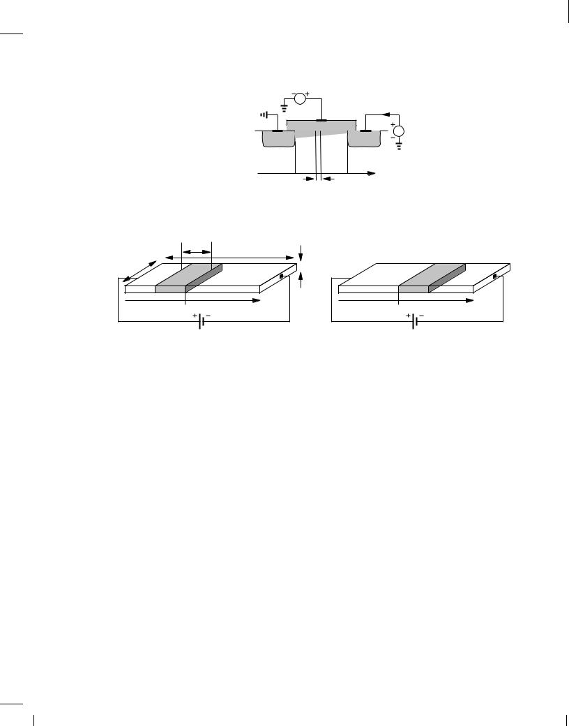
Figure 6.12 (a) Pinchoff, (b) variation of length with drain voltage, (c) detailed operation near the drain.
W
n+ |
n+ |
Figure 6.13 Illustration of capacitance per unit length.
Note that Q is expressed in coulomb/meter. Now recall from Fig. 6.11(a) that the channel voltage varies along the length of the transistor, and the charge density falls as we go from the source to the drain. Thus, Eq. (6.2) is valid only near the source terminal, where the channel potential remains close to zero. As shown in Fig. 6.14, we denote the channel potential at x by V (x) and write
Q(x) = W Cox[VGS , V (x) , VTH ]; |
(6.3) |
noting that V (x) goes from zero to VD if the channel is not pinched off.
Drain Current What is the relationship between the mobile charge density and the current? Consider a bar of semiconductor having a uniform charge density (per unit length) equal to Q and carrying a current I (Fig. 6.15). Note from Chapter 2 that (1) I is given by the total charge that passes through the cross section of the bar in one second, and (2) if the carriers move with a velocity of v m/s, then the charge enclosed in v meters along the bar passes through the cross
BR |
Wiley/Razavi/Fundamentals of Microelectronics [Razavi.cls v. 2006] |
June 30, 2007 at 13:42 |
292 (1) |
|
|
|
|
292 |
|
Chap. 6 |
Physics of MOS Transistors |
VG |
|
|
I D |
|
|
|
|
n+ |
|
n+ |
VD |
V ( x ) |
|
||
0 |
|
x |
|
dx |
L |
|
|
|
|
|
Figure 6.14 Device illustration for calculation of drain current.
section in one second. Since the charge enclosed in v meters is equal to Q v, we have
v |
t = t1 |
t = t1 + 1 s |
meters |
L |
|
|
|
|
W |
|
h |
x 1 |
x |
x |
|
x 1 |
|
V1 |
|
V1 |
Figure 6.15 Relationship between charge velocity and current.
I = Q v; |
|
(6.4) |
As explained in Chapter 2, |
|
|
v = , nE; |
|
(6.5) |
= + n dV |
; |
(6.6) |
dx |
|
|
where dV=dx denotes the derivative of the voltage at a given point. Combining (6.3), (6.4), and (6.6), we obtain
ID = W Cox[VGS , V (x) , VTH] n dV (x) |
: |
(6.7) |
dx |
|
|
Interestingly, since ID must remain constant along the channel (why?), V (x) and dV=dx must vary such that the product of VGS , V (x) , VTH and dV=dx is independent of x.
While it is possible to solve the above differential equation to obtain V (x) in terms of ID (and
the reader is encouraged to do that), our immediate need is to find an expression for |
ID in terms |
|||
of the terminal voltages. To this end, we write |
|
|||
|
x=L |
V (x)=VDS |
|
|
Z |
IDdx = Z |
|
nCoxW [VGS , V (x) , VTH]dV: |
(6.8) |
|
x=0 |
V (x)=0 |
|
|
That is, |
|
|
|
|
|
ID = 1 nCox W [2(VGS , VTH )VDS , V 2 ]: |
(6.9) |
||
|
2 |
L |
DS |
|
|
|
|
||
BR |
Wiley/Razavi/Fundamentals of Microelectronics [Razavi.cls v. 2006] |
June 30, 2007 at 13:42 |
293 (1) |
|
|
|
|
Sec. 6.2 Operation of MOSFET |
293 |
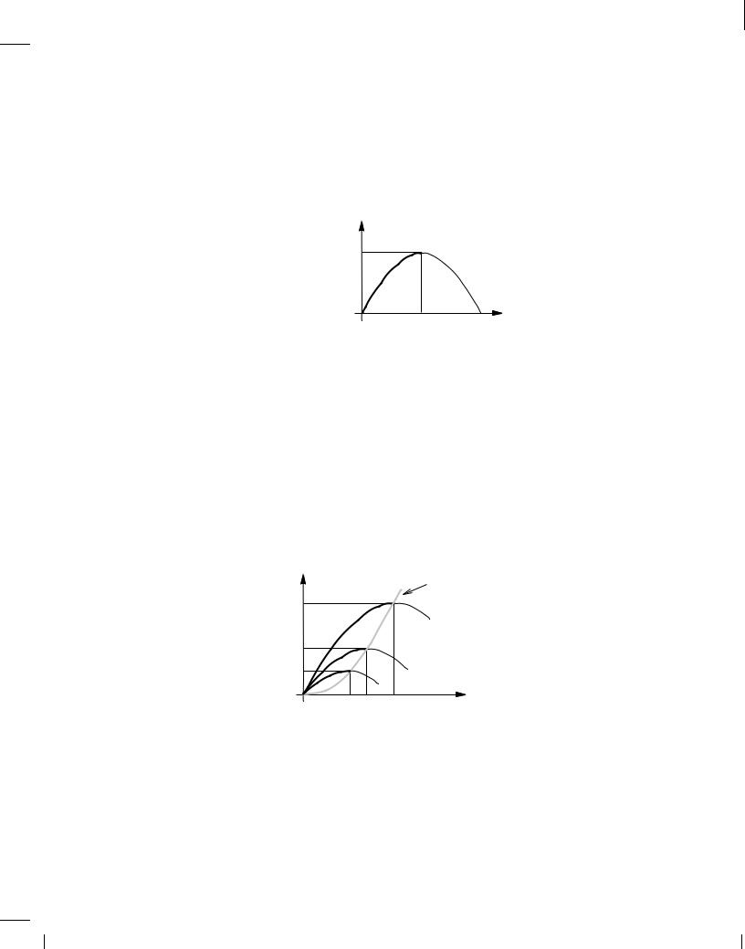
We now examine this important equation from different perspectives to gain more insight. First, the linear dependence of ID upon n, Cox, and W=L is to be expected: a higher mobility yields a greater current for a given drain-source voltage; a higher gate oxide capacitance leads to a larger electron density in the channel for a given gate-source voltage; and a larger W=L (called the device “aspect ratio”) is equivalent to placing more transistors in parallel [Fig. 6.10(c)]. Second, for a constant VGS, ID varies parabolically with VDS (Fig. 6.16), reaching a maximum of
|
|
|
|
|
|
I D |
||
1 |
n |
C |
W (V |
|
− V |
|
( |
2 |
2 |
|
ox L |
GS |
|
TH |
|
|
|
VGS − VTH
Figure 6.16 Parabolic ID-VDS characteristic.
ID;max = 12 nCox WL (VGS , VTH)2
VDS
(6.10)
at VDS = VGS ,VTH. It is common to write W=L as the ratio of two values e.g., 5 m=0:18 m (rather than 27.8) to emphasize the choice of W and L. While only the ratio appears in many MOS equations, the individual values of W and L also become critical in most cases. For example, if both W and L are doubled, the ratio remains unchanged but the gate capacitance increases.
Example 6.3
Plot the ID-VDS characteristics for different values of VGS.
Solution
As VGS increases, so do ID;max and VGS , VTH. Illustrated in Fig. 6.17, the characteristics exhibit maxima that follow a parabolic shape themselves because ID;max / (VGS , VTH )2.
Parabola
I D
I D,max4 |
VGS3 |
I D,max3 |
VGS2 |
|
|
I D,max2 |
VGS1 |
TH |
TH |
TH |
V− |
V− |
V− |
GS1 |
GS2 |
GS3 |
V |
V |
V |
VDS
Figure 6.17 MOS characteristics for different gate-source voltages.
Exercise
What happens to the above plots if tox is halved?
BR |
Wiley/Razavi/Fundamentals of Microelectronics [Razavi.cls v. 2006] |
June 30, 2007 at 13:42 |
294 (1) |
|
|
|
|
294 |
Chap. 6 |
Physics of MOS Transistors |
The nonlinear relationship between ID and VDS reveals that the transistor cannot generally be modeled as a simple linear resistor. However, if VDS 2(VGS , VTH ), Eq. (6.9) reduces to:
ID nCox W |
(VGS , VTH)VDS; |
(6.11) |
L |
|
|
exhibiting a linear ID-VDS behavior for a given VGS. In fact, the equivalent on-resistance is given by VDS=ID:
Ron = |
|
1 |
: |
(6.12) |
|
|
|||
W |
|
|||
|
|
|
|
|
|
nCox L |
(VGS , VTH ) |
|
|
From another perspective, at small VDS (near the origin), the parabolas in Fig. 6.17 can be approximated by straight lines having different slopes (Fig. 6.18).
I D |
|
VGS3 |
|
VGS3 |
|
|
I D |
||
|
|
|
VGS2 |
|
|
|
|
|
|
V |
GS2 |
|
|
VGS1 |
|
|
|
|
VGS1
VDS
VDS
Figure 6.18 Detailed characteristics for small VDS.
As predicted in Section 6.2.1, (6.12) suggests that the on-resistance can be controlled by the gate-source voltage. In particular, for VGS = VTH , Ron = 1, i.e., the device can operate as an electronic switch.
Example 6.4
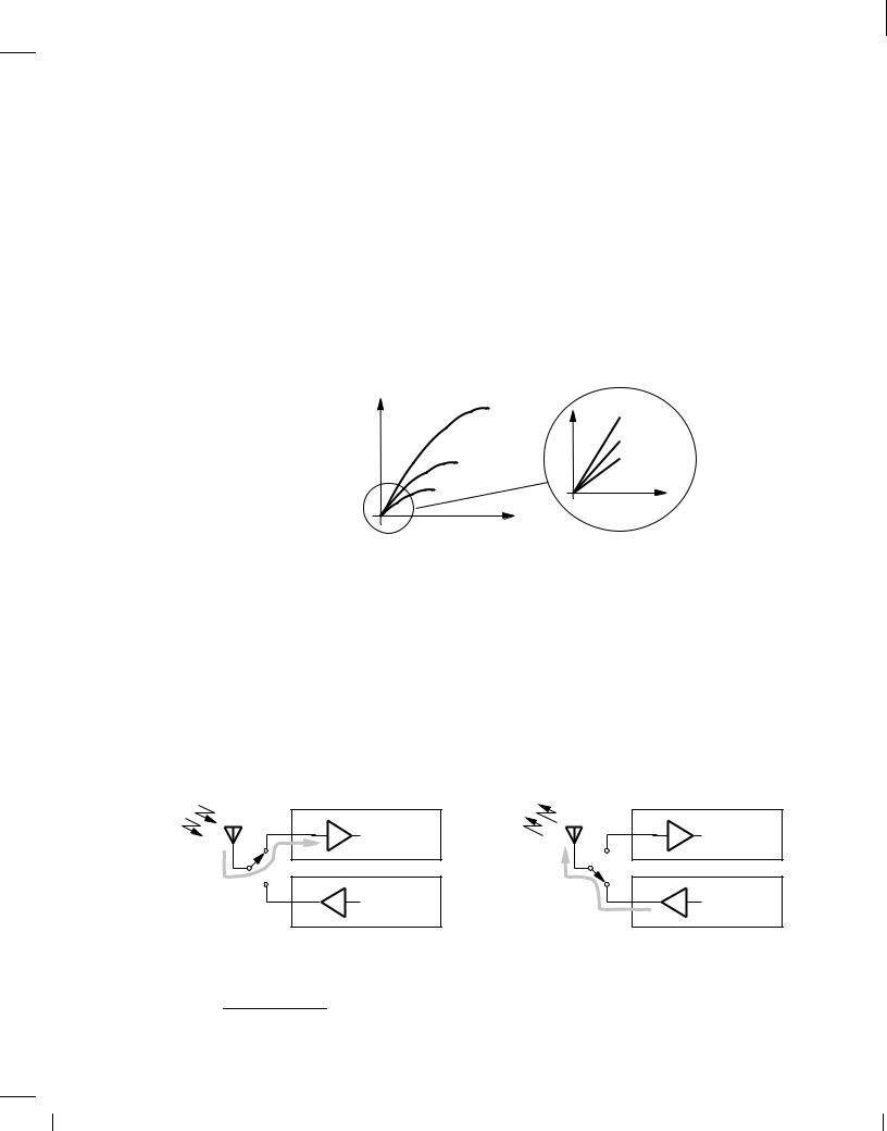
A cordless telephone incorporates a single antenna for reception and transmission. Explain how the system must be configured.
Solution
The system is designed such that the phone receives for half of the time and transmits for the other half. Thus, the antenna is alternately connected to the receiver and the transmitter in regular intervals, e.g., every 20 ms (Fig. 6.19). An electronic antenna switch is therefore necessary here.8
Receiver |
Receiver |
Transmitter |
Transmitter |
Figure 6.19 Role of antenna switch in a cordless phone.
8Some cellphones operate in the same manner.
BR |
Wiley/Razavi/Fundamentals of Microelectronics [Razavi.cls v. 2006] |
June 30, 2007 at 13:42 |
295 (1) |
|
|
|
|
Sec. 6.2 Operation of MOSFET |
295 |
Exercise
Some systems employ two antennas, each of which receives and transmits signals. How many switches are needed?
In most applications, it is desirable to achieve a low on-resistance for MOS switches. The circuit designer must therefore maximize W=L and VGS. The following example illustrates this point.
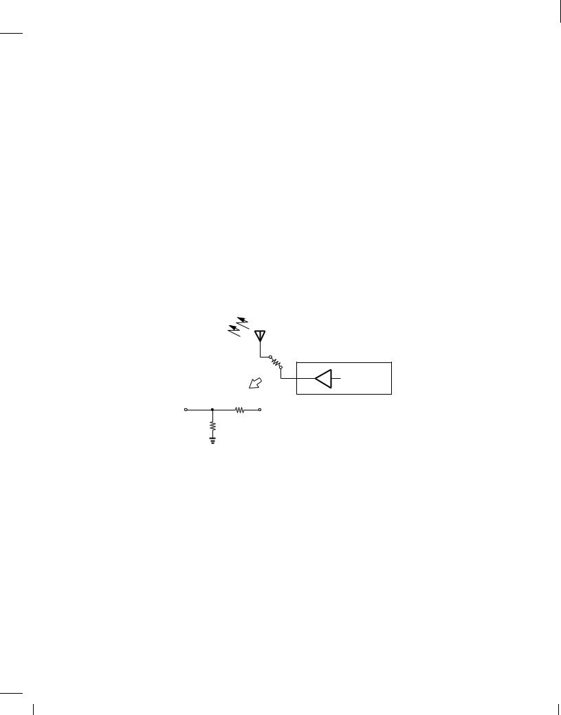
Example 6.5
In the cordless phone of Example 6.4, the switch connecting the transmitter to the antenna must negligibly attenuate the signal, e.g., by no more than 10%. If VDD = 1:8 V, nCox = 100 A=V2, and VTH = 0:4 V, determine the minimum required aspect ratio of the switch. Assume the antenna can be modeled as a 50resistor.
Solution
As depicted in Fig. 6.20, we wish to ensure
|
R on |
Ron |
Transmitter |
Vout |
Vin |
50 Ω Rant |
|
Figure 6.20 Signal degradation due to on-resistance of antenna switch.
Vout 0:9 |
(6.13) |
Vin |
|
and hence |
|
Ron 5:6 : |
(6.14) |
Setting VGS to the maximum value, VDD, we obtain from Eq. (6.12), |
|
W 1276: |
(6.15) |
L |
|
(Since wide transistors introduce substantial capacitance in the signal path, this choice of W=L may still attenuate high-frequency signals.)
BR |
Wiley/Razavi/Fundamentals of Microelectronics [Razavi.cls v. 2006] |
June 30, 2007 at 13:42 |
296 (1) |
|
|
|
|
296 |
Chap. 6 |
Physics of MOS Transistors |
Exercise
What W=L is necessary if VDD drops to 1.2 V?
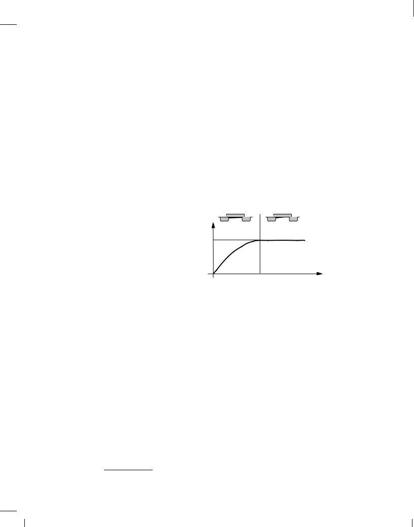
Triode and Saturation Regions Equation (6.9) expresses the drain current in terms of the device terminal voltages, implying that the current begins to fall for VDS > VGS , VTH. We say the device operates in the “triode region” 9 if VDS < VGS , VTH (the rising section of the parabola). We also use the term “deep triode region” for VDS 2(VGS , VTH ), where the transistor operates as a resistor.
In reality, the drain current reaches “saturation,” that is, becomes constant for VDS > VGS , VTH (Fig. 6.21). To understand why, recall from Fig. 6.12 that the channel experiences pinch-off if VDS = VGS , VTH. Thus, further increase in VDS simply shifts the pinch-off point slightly toward the drain. Also, recall that Eqs. (6.7) and (6.8) are valid only where channel charge exists. It follows that the integration in (6.8) must encompass only the channel, i.e., from x = 0 to x = L1 in Fig. 6.12(b), and be modified to
|
|
|
|
|
|
I D |
Triode |
||
1 |
|
C |
W (V |
|
− V |
|
( |
2 |
Region |
n |
|
|
|
||||||
2 |
|
ox L |
GS |
|
TH |
|
|
|
|
VGS
Figure 6.21 Overall MOS characteristic.
Saturation
Region
− VTH
VDS
|
x=L1 |
V (x)=VGS,VTH |
|
Z |
IDdx = Z |
nCoxW [VGS , V (x) , VTH ]dV: |
(6.16) |
|
x=0 |
V (x)=0 |
|
Note that the upper limits correspond to the channel pinch-off point. In particular, the integral on the right hand side is evaluated up to VGS , VTH rather than VDS. Consequently,
ID = |
1 |
nCox W (VGS , VTH)2; |
(6.17) |
|
2 |
L1 |
|
a result independent of VDS and identical to ID;max in (6.10) if we assume L1 L. Called the “overdrive voltage,” the quantity VGS , VTH plays a key role in MOS circuits. MOSFETs are sometimes called “square-law” devices to emphasize the relationship between ID and the overdrive. For the sake of brevity, we hereafter denote L1 with L.
The I-V characteristic of Fig. 6.21 resembles that of bipolar devices, with the triode and saturation regions in MOSFETs appearing similar to saturation and forward active regions in bipolar transistors, respectively. It is unfortunate that the term “saturation” refers to completely different regions in MOS and bipolar I-V characteristics.
9Also called the “linear region.”
BR |
Wiley/Razavi/Fundamentals of Microelectronics [Razavi.cls v. 2006] |
June 30, 2007 at 13:42 |
297 (1) |
|
|
|
|
Sec. 6.2 Operation of MOSFET |
297 |
We employ the conceptual illustration in Fig. 6.22 to determine the region of operation. Note that the gate-drain potential difference suits this purpose and we need not compute the gatesource and gate-drain voltages separately.
VTH
> VTH
|
|
|
|
|
|
I D |
|
1 µ |
|
C |
W (V |
|
− V |
|
2 |
n |
|
|
( |
||||
2 |
|
ox L |
GS |
|
TH |
|
|
Triode |
Saturation |
Region |
Region |
VGS |
− VTH |
(a)
Saturated


 M 1
M 1
VDS
(b)
Figure 6.22 Illustration of triode and saturation regions based on the gate and drain voltages.
Exhibiting a “flat” current in the saturation region, a MOSFET can operate as a current source having a value given by (6.17). Furthermore, the square-law dependence of ID upon VGS ,VTH suggests that the device can act as a voltage-controlled current source.
Example 6.6
Calculate the bias current of M1 in Fig. 6.23. Assume nCox = 100 A=V2 and VTH = 0:4 V. If the gate voltage increases by 10 mV, what is the change in the drain voltage?
|
|
|
|
|
|
|
|
|
|
|
|
|
|
|
|
|
|
VDD = 1.8 V |
|||
|
|
|
|
|
|
|
|
|
|
|
|
|
|
|
|
|
|
||||
|
|
|
|
|
|
|
|
|
|
|
R D |
|
|
5 kΩ |
|
|
|||||
|
|
|
|
|
|
|
|
|
|
|
I D |
|
|
|
|
|
|
||||
|
|
|
|
|
|
|
|
|
|
|
|
|
|
|
|
|
X |
W |
|
2 |
|
|
|
|
|
|
|
|
|
|
|
|
|
|
|
|
|
M |
1 |
= |
|
||
1 V |
|
|
|
|
|
|
|
|
|
|
|
|
|
|
|
|
|
L |
|
0.18 |
|
|
|
|
|
|
|
|
|
|
|
|
|
|
|
|
|
|
|
|
|
|
|
|
|
|
|
|
|
|
|
|
|
|
|
|
|
|
|
|
|
|
|
|
|
|
|
|
|
|
|
|
|
|
|
|
|
|
|
|
|
|
|
|
|
|
|
|
|
|
|
|
|
|
|
|
|
|
|
|
|
|
|
|
|
|
|
|
|
Figure 6.23 Simple MOS circuit.
Solution
It is unclear a priori in which region M1 operates. Let us assume M1 is saturated and proceed. Since VGS = 1 V,
ID = 1 |
nCox W (VGS , VTH )2 |
(6.18) |
2 |
L |
|
= 200 A: |
(6.19) |
|
We must check our assumption by calculating the drain potential: |
|
|
VX = VDD , RDID |
(6.20) |
|
|
= 0:8 V: |
(6.21) |

BR |
Wiley/Razavi/Fundamentals of Microelectronics [Razavi.cls v. 2006] |
June 30, 2007 at 13:42 |
298 (1) |
|
|
|
|
298 |
Chap. 6 |
Physics of MOS Transistors |
|
The drain voltage is lower than the gate voltage, but by less than VTH. The illustration in Fig. |
|
|
6.22 therefore indicates that M1 indeed operates in saturation. |
|
|
If the gate voltage increases to 1.01 V, then |
|
|
ID = 206:7 A; |
(6.22) |
|
lowering VX to |
|
|
VX = 0:766 V: |
(6.23) |
Fortunately, M1 is still saturated. The 34-mV change in VX reveals that the circuit can amplify the input.
Exercise
What choice of RD places the transistor at the edge of the triode region?
It is instructive to identify several points of contrast between bipolar and MOS devices. (1) A bipolar transistor with VBE = VCE resides at the edge of the active region whereas a MOSFET approaches the edge of saturation if its drain voltage falls below its gate voltage by VTH. (2) Bipolar devices exhibit an exponential IC-VBE characteristic while MOSFETs display a squarelaw dependence. That is, the former provide a greater transconductance than the latter (for a given bias current). (3) In bipolar circuits, most transistors have the same dimensions and hence the same IS, whereas in MOS circuits, the aspect ratio of each device may be chosen differently to satisfy the design requirements. (4) The gate of MOSFETs draws no bias current.10
Example 6.7
Determine the value of W=L in Fig. 6.23 that places M1 at the edge of saturation and calculate the drain voltage change for a 1-mV change at the gate. Assume VTH = 0:4 V.
Solution
With VGS = +1 V, the drain voltage must fall to VGS , VTH = 0:6 V for M1 to enter the triode region. That is,
ID = VDD |
, VDS |
(6.24) |
||||||
|
RD |
|
|
|
|
|||
= 240 A: |
|
|
|
(6.25) |
||||
Since ID scales linearly with W=L, |
|
|
|
|
|
|
|
|
W jmax = |
240 |
A |
|
2 |
|
(6.26) |
||
200 |
A |
0:18 |
||||||
L |
|
|
||||||
= |
2:4 |
|
: |
|
|
|
(6.27) |
|
|
|
|
|
|
||||
|
0:18 |
|
|
|
|
|||
If VGS increases by 1 mV, |
|
|
|
|
|
|
|
|
ID = 248:04 A; |
(6.28) |
|||||||
10New generations of MOSFETs suffer from gate “leakage” current, but we neglect this effect here.
BR |
Wiley/Razavi/Fundamentals of Microelectronics [Razavi.cls v. 2006] |
June 30, 2007 at 13:42 |
299 (1) |
|
|
|
|
Sec. 6.2 Operation of MOSFET |
299 |
changing VX by |
|
VX = ID RD |
(6.29) |
= 4:02 mV: |
(6.30) |
The voltage gain is thus equal to 4.02 in this case.
Exercise
Repeat the above example if RD is doubled.
Example 6.8
Calculate the maximum allowable gate voltage in Fig. 6.24 if M1 must remain saturated.
|
|
|
|
|
|
|
|
|
|
|
VDD = 1.8 V |
||
|
|
|
|
|
|
|
|
|
|
|
|||
|
R D |
|
|
|
|
5 kΩ |
|
|
|||||
|
|
|
|||||||||||
|
I D |
|
|
|
|
|
|
|
|||||
|
|
|
|
|
|
|
|
|
|
X |
|
|
|
VGS |
|
|
|
|
|
|
|
M 1 W |
= |
2 |
|||
|
|
|
|
|
|
|
|||||||
|
|
|
|
|
|
|
|
|
|
|
L |
|
0.18 |
|
|
|
|
|
|
|
|
|
|
|
|
|
|
Figure 6.24 Simple MOS circuit.
Solution
At the edge of saturation, VGS ,VTH = VDS = VDD , RDID: Substituting for ID from (6.17) gives
VGS , VTH |
= VDD |
, |
RD |
nCox W |
(VGS , VTH )2; |
(6.31) |
||||||||||||||
|
|
|||||||||||||||||||
|
|
|
|
|
2 |
|
|
|
L |
|
|
|
|
|
|
|
|
|
|
|
and hence |
|
|
|
|
|
|
|
|
|
|
|
|
|
|
|
|
|
|
|
|
|
|
|
|
|
|
|
|
|
|
|
|
|
|
|
|
|
||||
|
|
1 + |
1 + 2RDVDD nCox |
W |
|
|
|
|||||||||||||
|
|
L |
|
(6.32) |
||||||||||||||||
VGS , VTH = |
, |
|
q |
|
|
|
|
|
|
|
|
|
|
: |
||||||
|
|
RD nCox |
W |
|
|
|
|
|
||||||||||||
|
|
|
|
|
|
|
|
L |
|
|
|
|
|
|||||||
|
|
|
|
|
|
|
|
|
|
|
|
|
|
|
|
|
||||
Thus, |
|
|
|
|
|
|
|
|
|
|
|
|
|
|
|
|
|
|
|
|
|
|
|
|
|
|
|
|
|
|
|
|
|
||||||||
|
|
1 + 1 + 2RDVDD nCox |
W |
|
|
|
|
|
|
|||||||||||
|
|
|
|
|
|
|
(6.33) |
|||||||||||||
VGS = |
, |
q |
|
|
|
|
|
|
|
|
|
L |
+ VTH: |
|||||||
|
|
|
|
W |
|
|
|
|
|
|
||||||||||
|
|
|
|
RD nCox |
|
|
|
|
|
|
|
|
|
|
|
|||||
|
|
|
|
L |
|
|
|
|
|
|
|
|
|
|
||||||
Exercise
Calculate the value of VGS if munCox = 100 A=V2 and VTH = 0:4
BR |
Wiley/Razavi/Fundamentals of Microelectronics [Razavi.cls v. 2006] |
June 30, 2007 at 13:42 |
300 (1) |
|
|
|
|
300 |
Chap. 6 |
Physics of MOS Transistors |
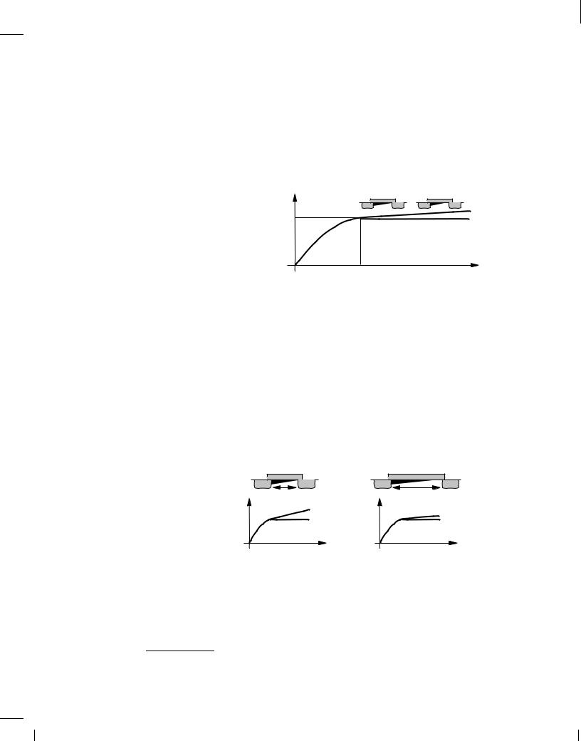
6.2.3 Channel-Length Modulation
In our study of the pinch-off effect, we observed that the point at which the channel vanishes in fact moves toward the source as the drain voltage increases. In other words, the value of L1 in Fig. 6.12(b) varies with VDS to some extent. Called “channel-length modulation” and illustrated in Fig. 6.25, this phenomenon yields a larger drain current as VDS increases because ID / 1=L1 in Eq. (6.17). Similar to the Early effect in bipolar devices, channel-length modulation results in a finite output impedance given by the inverse of the ID-VDS slope in Fig. 6.25.
|
|
|
|
|
|
I D |
||
1 |
n |
C |
W (V |
|
− V |
|
( |
2 |
2 |
|
ox L |
GS |
|
TH |
|
|
|
VGS
Figure 6.25 Variation of ID in saturation region.
−
VTH
VDS
To account for channel-length modulation, we assume L is constant, but multiply the right hand side of (6.17) by a corrective term:
ID = |
1 |
nCox W |
(VGS , VTH)2(1 + VDS); |
(6.34) |
|
2 |
L |
|
|
where is called the “channel-length modulation coefficient.” While only an approximation, this linear dependence of ID upon VDS still provides a great deal of insight into the circuit design implications of channel-length modulation.
Unlike the Early effect in bipolar devices (Chapter 4), the amount of channel-length modulation is under the circuit designer's control. This is because is inversely proportional to L: for a longer channel, the relative change in L (and hence in ID) for a given change in VDS is smaller (Fig. 6.26).11 (By contrast, the base width of bipolar devices cannot be adjusted by the circuit designer, yielding a constant Early voltage for all transistors in a given technology.)
L 1 |
L 2 |
I D |
I D |
VDS |
VDS |
Figure 6.26 Channel-length modulation.
Example 6.9
A MOSFET carries a drain current of 1 mA with VDS = 0:5 V in saturation. Determine the change in ID if VDS rises to 1 V and = 0:1 V,1. What is the device output impedance?
11Since different MOSFETs in a circuit may be sized for different 's, we do not define a quantity similar to the Early voltage here.