

Fundamentals of Microelectronics
.pdfBR |
Wiley/Razavi/Fundamentals of Microelectronics [Razavi.cls v. 2006] |
June 30, 2007 at 13:42 |
171 (1) |
|
|
|
|
Sec. 4.7 |
Chapter Summary |
|
|
|
|
|
|
|
|
|
|
171 |
|||||||||||
|
|
|
|
|
|
360 k Ω |
|
|
|
|
|
|
|
|
|
|
|
|
|
|
|
|
|
|
|
|
|
Q 1 |
|
|
|
|
|
|
|
|
|
|
|||||||||
|
|
|
|
|
|
|
|
|
|
|
|
|
|
||||||||||
|
|
|
|
|
|
|
|
|
|
|
|
|
|
|
|
|
|
|
|
|
|||
|
|
|
|
|
|
RB |
|
|
|
|
|
|
|||||||||||
|
|
|
|
|
|
|
|
|
|
|
|
|
|
|
|||||||||
|
|
|
|
|
|
|
|
|
|
|
VCC |
|
|
|
|
|
|
|
|
|
2.5 V |
||
|
|
|
|
|
|
|
|
|
|
|
|
|
|
|
|
|
|
|
|||||
|
|
|
|
|
|
|
|
|
|
|
|
|
|
|
|
|
|
|
|||||
Figure 4.79 |
|
|
|
|
|
|
|
|
|
|
|
|
4 kΩ |
|
|
|
|
|
|
||||
|
|
|
|
|
|
|
|
|
|
|
|
|
|||||||||||
|
|
|
|
|
|
|
|
|
|
|
|
|
|||||||||||
|
|
|
|
|
|
|
|
|
|
|
|
|
|
|
|
|
|
|
|
|
|
|
|
|
|
|
|
|
|
|
|
|
|
|
|
|
|
|
|
|
|
|
|
|
|
|
|
|
|
|
|
|
|
|
|
|
|
|
|
|
|
|
|
|
|
|
|
|
|
|
|
(a)Determine IS such that Q1 experiences a collector-base forward bias of 200 mV.
(b)Calculate the transconductance of the transistor.
52.Determine the region of operation of Q1 in each of the circuits shown in Fig. 4.80. Assume
IS = 5 10,16 A, = 100, VA = 1.
RE |
|
RB |
RE |
|
|
|
|
|
|
|
|
Q 1 |
|
Q 1 |
|
|
Q 1 |
|
VCC |
2.5 V |
VCC |
2.5 V |
|
VCC |
2.5 V |
300 Ω |
|
RC |
|
|
RC |
|
1 kΩ |
|
|
|
|
|
|
|
|
(a) |
|
|
(b) |
|
(c) |
|
|
RE |
|
|
|
|
|
|
|
|
0.5 mA |
VCC |
2.5 V |
|
|
Q 1 |
|
|
|
|
|
|
VCC |
2.5 V |
|
Q 1 |
|
|
|
RC |
|
|
500 Ω |
|
|
|
|
|
|
|
|
|
|
(d) |
|
|
(e) |
|
|
Figure 4.80 |
|
|
|
|
|
|
53. Consider the circuit shown in Fig. 4.81, where, IS1 = 3IS2 = 5 10,16 A, 1 |
= 100, |
|||||
2 = 50, VA = 1, and RC = 500 . |
|
|
|
|||
|
|
|
Q 1 |
VCC = 2.5 V |
|
|
|
|
Vin |
|
|
||
|
|
|
|
|
|
|
|
|
|
Q 2 |
|
|
|
|
|
|
Vout |
|
|
|
|
|
|
RC |
|
|
|
Figure 4.81 |
|
|
|
|
|
|
(a) We wish to forward-bias the collector-base junction of Q2 by no more than 200 mV. What is the maximum allowable value of Vin?
BR |
Wiley/Razavi/Fundamentals of Microelectronics [Razavi.cls v. 2006] |
June 30, 2007 at 13:42 |
172 (1) |
|
|
|
|
172 Chap. 4 Physics of Bipolar Transistors
(b) With the value found in (a), calculate the small-signal parameters of Q1 and Q2 and construct the equivalent circuit.
54.Repeat Problem 53 for the circuit depicted in Fig. 4.82 but for part (a), determine the minimum allowable value of Vin. Verify that Q1 operates in the active mode.
Q 1 |
VCC |
= 2.5 V |
|
Vin |
|||
|
|
||
Q 2 |
|
|
|
|
Vout |
|
RC
Figure 4.82
55. Repeat Problem 53 for the circuit illustrated in Fig. 4.83.
|
VCC = 2.5 V |
|
R C |
Q 1 |
Vout |
Vin |
Q 2 |
Figure 4.83
56. In the circuit of Fig. 4.84, IS1 = 2IS2 = 6 10,17 A, 1 = 80 and 2 = 100.
|
VCC = 2.5 V |
|
R C |
Q 1 |
Vout |
Vin |
Q 2 |
Figure 4.84 |
|
(a)What value of Vin yields a collector current of 2 mA for Q2?
(b)With the value found in (a), calculate the small-signal parameters of Q1 and Q2 and construct the equivalent circuit.
SPICE Problems
In the following problems, assume IS;npn = 5 10,16 A, npn = 100, VA;npn = 5 V,
IS;pnp = 8 10,16 A, pnp = 50, VA;pnp = 3:5 V.
57.Plot the input/output characteristic of the circuit shown in Fig. 4.85 for 0 < Vin < 2:5 V. What value of Vin places the transistor at the edge of saturation?
58.Repeat Problem 57 for the stage depicted in Fig. 4.86. At what value of Vin does Q1 carry a collector current of 1 mA?
59.Plot IC1 and IC2 as a function of Vin for the circuits shown in Fig. 4.87 for 0 < Vin < 1:8 V. Explain the dramatic difference between the two.
BR |
Wiley/Razavi/Fundamentals of Microelectronics [Razavi.cls v. 2006] |
June 30, 2007 at 13:42 |
173 (1) |
|
|
|
|
Sec. 4.7 |
Chapter Summary |
173 |
||||||||||||||||||||||
|
|
|
|
|
|
|
|
|
|
|
|
|
|
|
|
|
|
|
|
|
|
|||
|
|
|
|
|
|
|
|
|
|
R C |
|
1 kΩ |
|
|
|
|
|
|
|
|
||||
|
|
|
|
|
|
|
|
|
|
|
|
|
|
|
|
|
|
|
||||||
|
|
|
|
|
||||||||||||||||||||
|
|
|
|
|
|
|
|
|
|
|
|
|
|
Vout |
|
|
|
|
|
|
|
|
|
VCC = 2.5 V |
|
|
|
|
|
|
|
|
|
|
|
|
|
|
|
|
|
|
|
|
|
|
|
||
|
|
|
|
|
|
|
|
|
|
|
|
|
|
|
|
|
|
|
|
|
|
|
|
|
|
VB = 0.9 V |
|
|
|
|
|
|
|
|
|
|
|
Q 1 |
|||||||||||
|
|
|
|
|
|
|
|
|
|
|
|
|||||||||||||
|
|
|
|
|
|
|
|
|
|
|
||||||||||||||
|
|
|
|
|
|
|
|
|
|
|
|
|
|
|
|
|
|
|
|
|
||||
Figure 4.85 |
|
|
|
|
|
|
|
|
|
|
|
Vin |
||||||||||||
|
|
|
|
|
|
|
|
|
|
|
||||||||||||||
|
|
|
|
|
|
|
|
|
|
|
||||||||||||||
|
|
|
|
|
|
|
|
|
|
|
||||||||||||||
|
|
|
|
|
|
|
|
|
|
|
||||||||||||||
|
|
|
|
|
|
|
|
|
|
|
|
|
|
|
|
|
|
|
|
|
|
|
|
|
 VCC = 2.5 V
Vin

 Q 1
Q 1

 Vout
Vout
1 kΩ
Figure 4.86
I C2 |
VCC |
= 2.5 V |
|
I C1 |
VCC |
= 2.5 V |
Vin |
Q 2 |
|
|
|
Vin

 Q 1
Q 1

 Q 3
Q 3
(a) |
(b) |
Figure 4.87
60.Plot the input/output characteristic of the circuit illustrated in Fig. 4.88 for 0 < Vin < 2 V. What value of Vin yields a transconductance of (50 ),1 for Q1?
R C |
1 kΩ |
VCC |
= 2.5 V |
|
Vout |
||
|
|
|

 Q 1
Q 1
Vin
Q 2
Figure 4.88
61.Plot the input/output characteristic of the stage shown in Fig. 4.89 for 0 < Vin < 2:5 V. At what value of Vin do Q1 and Q2 carry equal collector currents? Can you explain this result intuitively?
BR |
Wiley/Razavi/Fundamentals of Microelectronics [Razavi.cls v. 2006] |
June 30, 2007 at 13:42 |
174 (1) |
|
|
|
|
174 |
|
Chap. 4 |
Physics of Bipolar Transistors |
Vin |
Q 1 |
1 kΩ |
VCC = 2.5 V |
Vout |
|
||
|
|
|
|
|
|
Q 2 |
|
|
|
1.5 V |
|
|
1 kΩ |
|
|
Figure 4.89 |
|
|
|
BR |
Wiley/Razavi/Fundamentals of Microelectronics [Razavi.cls v. 2006] |
June 30, 2007 at 13:42 |
175 (1) |
|
|
|
|
Bipolar Amplifiers
With the physics and operation of bipolar transistors described in Chapter 4, we now deal with amplifier circuits employing such devices. While the field of microelectronics involves much more than amplifiers, our study of cellphones and digital cameras in Chapter 1 indicates the extremely wide usage of amplification, motivating us to master the analysis and design of such building blocks. This chapter proceeds as follows.
General Concepts |
Operating Point Analysis |
Amplifier Topologies |
Input and Output Impedances |
Simple Biasing |
Common−Emitter Stage |
Biasing |
Emitter Degeneration |
Common−Base Stage |
DC and Small−Signal Analysis |
Self−Biasing |
Emtter Follower |
|
Biasing of PNP Devices |
|
Building the foundation for the remainder of this book, this chapter is quite long. Most of the concepts introduced here are invoked again in Chapter 7 (MOS amplifiers). The reader is therefore encouraged to take frequent breaks and absorb the material in small doses.
5.1 General Considerations
Recall from Chapter 4 that a voltage-controlled current source along with a load resistor can form an amplifier. In general, an amplifier produces an output (voltage or current) that is a magnified version of the input (voltage or current). Since most electronic circuits both sense and produce voltage quantities,1 our discussion primarily centers around “voltage amplifiers” and the concept of “voltage gain,” vout=vin.
What other aspects of an amplifier's performance are important? Three parameters that readily come to mind are (1) power dissipation (e.g., because it determines the battery lifetime in a cellphone or a digital camera); (2) speed (e.g., some amplifiers in a cellphone or analog-to-digital converters in a digital camera must operate at high frequencies); (3) noise (e.g., the front-end amplifier in a cellphone or a digital camera processes small signals and must introduce negligible noise of its own).
1Exceptions are described in Chapter 12.
175
BR |
Wiley/Razavi/Fundamentals of Microelectronics [Razavi.cls v. 2006] |
June 30, 2007 at 13:42 |
176 (1) |
|
|
|
|
176 |
Chap. 5 |
Bipolar Amplifiers |
5.1.1 Input and Output Impedances
In addition to the above parameters, the input and output (I/O) impedances of an amplifier play a critical role in its capability to interface with preceding and following stages. To understand this concept, let us first determine the I/O impedances of an ideal voltage amplifier. At the input, the circuit must operate as a voltmeter, i.e., sense a voltage without disturbing (loading) the preceding stage. The ideal input impedance is therefore infinite. At the output, the circuit must behave as a voltage source, i.e., deliver a constant signal level to any load impedance. Thus, the ideal output impedance is equal to zero.
In reality, the I/O impedances of a voltage amplifier may considerably depart from the ideal values, requiring attention to the interface with other stages. The following example illustrates the issue.
Example 5.1
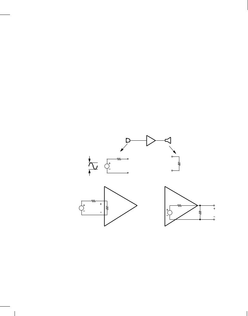
An amplifier with a voltage gain of 10 senses a signal generated by a microphone and applies the amplified output to a speaker [Fig. 5.1(a)]. Assume the microphone can be modeled with a voltage source having a 10-mV peak-to-peak signal and a series resistance of 200 . Also assume the speaker can be represented by an 8- resistor.
|
|
|
Microphone |
Amplifier Speaker |
|
|
|
|
|
A v = 10 |
|
|
|
|
200 Ω |
|
|
10 mV |
|
v m |
R m |
8 Ω |
|
|
|
|
|
||
|
|
|
|
(a) |
|
|
200 Ω |
|
Ramp |
|
|
|
R m |
|
|
|
|
v m |
v 1 |
Rin |
|
|
|
|
v amp |
R L 8 Ω v out |
|||
|
|
|
|
||
(b) |
(c) |
Figure 5.1 (a) Simple audio system, (b) signal loss due to amplifier input impedance, (c) signal loss due to amplifier output impedance.
(a)Determine the signal level sensed by the amplifier if the circuit has an input impedance of 2 k or 500 .
(b)Determine the signal level delivered to the speaker if the circuit has an output impedance of 10 or 2 .
Solution
(a) Figure 5.1(b) shows the interface between the microphone and the amplifier. The voltage

BR |
Wiley/Razavi/Fundamentals of Microelectronics [Razavi.cls v. 2006] |
June 30, 2007 at 13:42 |
177 (1) |
|
|
|
|
Sec. 5.1 General Considerations 177
sensed by the amplifier is therefore given by
v1 = |
Rin |
vm: |
(5.1) |
|
Rin + Rm |
||||
|
|
|
||
For Rin = 2 k , |
|
|
|
|
v1 |
= 0:91vm; |
(5.2) |
||
only 9% less than the microphone signal level. On the other hand, for Rin = 500 , |
|
|||
v1 |
= 0:71vm; |
(5.3) |
||
i.e., nearly 30% loss. It is therefore desirable to maximize the input impedance in this case.
(b) Drawing the interface between the amplifier and the speaker as in Fig. 5.1(c), we have
|
RL |
(5.4) |
|
vout = |
|
vamp: |
|
RL + Ramp |
|||
For Ramp = 10 , |
|
||
vout = 0:44vamp; |
(5.5) |
||
a substantial attenuation. For Ramp = 2 , |
|
||
vout = 0:8vamp: |
(5.6) |
||
Thus, the output impedance of the amplifier must be minimized. |
|
||
Exercise
If the signal delivered to the speaker is equal to 0:2vm, find the ratio of Rm and RL.
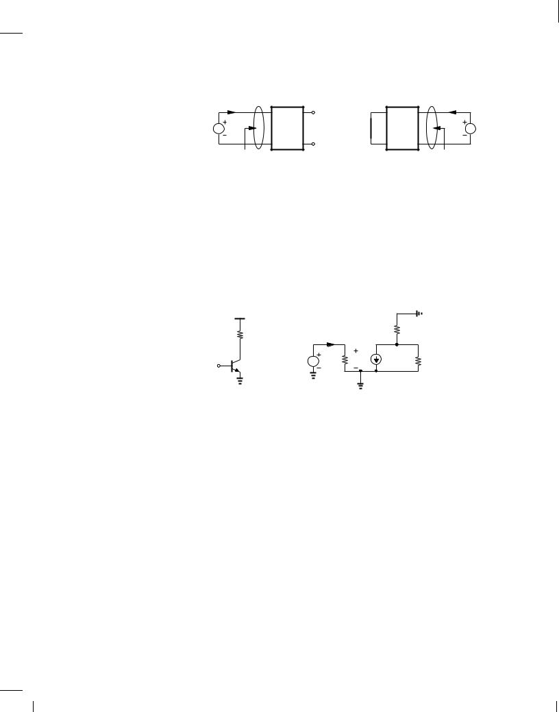
The importance of I/O impedances encourages us to carefully prescribe the method of measuring them. As with the impedance of two-terminal devices such as resistors and capacitors, the input (output) impedance is measured between the input (output) nodes of the circuit while all independent sources in the circuit are set to zero.2 Illustrated in Fig. 5.2, the method involves applying a voltage source to the two nodes (also called “port”) of interest, measuring the resulting current, and defining vX =iX as the impedance. Also shown are arrows to denote “looking into” the input or output port and the corresponding impedance.
The reader may wonder why the output port in Fig. 5.2(a) is left open whereas the input port in Fig. 5.2(b) is shorted. Since a voltage amplifier is driven by a voltage source during normal operation, and since all independent sources must be set to zero, the input port in Fig. 5.2(b) must be shorted to represent a zero voltage source. That is, the procedure for calculating the output impedance is identical to that used for obtaining the Thevenin impedance of a circuit (Chapter 1). In Fig. 5.2(a), on the other hand, the output remains open because it is not connected to any external sources.
2Recall that a zero voltage source is replaced by a short and a zero current source by an open.
BR |
Wiley/Razavi/Fundamentals of Microelectronics [Razavi.cls v. 2006] |
June 30, 2007 at 13:42 |
178 (1) |
|
|
|
|
178 |
Chap. 5 |
Bipolar Amplifiers |
|
Input |
|
Output |
|
Port |
|
Port |
i X |
i X |
|
|
|
v x |
Short |
|
v X |
R in |
|
R out |
|
(a) |
|
(b) |
|
Figure 5.2 Measurement of (a) input and (b) output impedances.
Determining the transfer of signals from one stage to the next, the I/O impedances are usually regarded as small-signal quantities—with the tacit assumption that the signal levels are indeed small. For example, the input impedance is obtained by applying a small change in the input voltage and measuring the resulting change in the input current. The small-signal models of semiconductor devices therefore prove crucial here.
Example 5.2
Assuming that the transistor operates in the forward active region, determine the input impedance of the circuit shown in Fig. 5.3(a).
|
VCC |
|
|
|
|
R C |
i X |
R C |
|
|
|
|
||
v in |
v X |
r π vπ |
gm vπ |
r O |
Q 1 |
|
|
|
|
|
(a) |
(b) |
|
|
Figure 5.3 (a) Simple amplifier stage, (b) small-signal model.
Solution
Constructing the small-signal equivalent circuit depicted in Fig. 5.3(b), we note that the input impedance is simply given by
vx = r : |
(5.7) |
ix |
|
Since r = =gm = VT =IC, we conclude that a higher or lower IC yield a higher input impedance.
Exercise
What happens if RC is doubled?
To simplify the notations and diagrams, we often refer to the impedance seen at a node rather than between two nodes (i.e., at a port). As illustrated in Fig. 5.4, such a convention simply assumes that the other node is the ground, i.e., the test voltage source is applied between the node of interest and ground.
BR |
Wiley/Razavi/Fundamentals of Microelectronics [Razavi.cls v. 2006] |
June 30, 2007 at 13:42 |
179 (1) |
|
|
|
|
Sec. 5.1 |
General Considerations |
179 |
|
|
Short |
|
R in |
R out |
|
(a) |
(b) |
Figure 5.4 Concept of impedance seen at a node.
Example 5.3
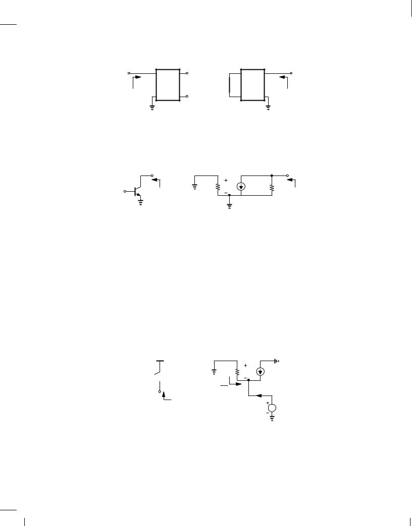
Calculate the impedance seen looking into the collector of Q1 in Fig. 5.5(a).
v in |
r π |
vπ |
gm vπ |
r O |
R out |
Q 1 R out |
|
|
|
||
|
(a) |
(b) |
|
|
|
Figure 5.5 (a) Impedance seen at collector, (b) small-signal model.
Solution
Setting the input voltage to zero and using the small-signal model in Fig. 5.5(b), we note that v = 0, gmv = 0, and hence Rout = rO.
Exercise
What happens if a resistance of value R1 is placed in series with the base?
Example 5.4
Calculate the impedance seen at the emitter of Q1 simplicity.
VCC
v in

 Q 1
Q 1
R out
(a)
in Fig. 5.6(a). Neglect the Early effect for
r π vπ |
gm vπ |
vπ |
|
r π |
i X |
|
v X |
|
(b) |
Figure 5.6 (a) Impedance seen at emitter, (b) small-signal model.
Solution
Setting the input voltage to zero and replacing VCC with ac ground, we arrive at the small-signal
BR |
Wiley/Razavi/Fundamentals of Microelectronics [Razavi.cls v. 2006] |
June 30, 2007 at 13:42 |
180 (1) |
|
|
|
|
180 Chap. 5 Bipolar Amplifiers
circuit shown in Fig. 5.6(b). Interestingly, v = ,vX and |
|
|
|||||||
g v |
|
+ v |
= ,i |
X |
: |
(5.8) |
|||
m |
|
r |
|
|
|
|
|||
|
|
|
|
|
|
|
|
|
|
That is, |
|
|
|
|
|
|
|
|
|
vX = |
|
1 |
|
|
: |
|
(5.9) |
||
|
|
1 |
|
|
|||||
iX |
|
|
|
|
|
|
|||
|
|
|
gm + r |
|
|
|
|
||
Since r = =gm 1=gm, we have Rout 1=gm.
Exercise
What happens if a resistance of value R1 is placed in series with the collector?
The above three examples provide three important rules that will be used throughout this book (Fig. 5.7): Looking into the base, we see r if the emitter is (ac) grounded. Looking into the collector, we see rO if the emitter is (ac) grounded. Looking into the emitter, we see 1=gm if the base is (ac) grounded and the Early effect is neglected. It is imperative that the reader master these rules and be able to apply them in more complex circuits.3
|
|
r O |
|
|
|
|
VA = |
r π |
ac |
ac ac |
|
|
|
ac |
1 |
|
|
|
|
|
|
|
g m |
Figure 5.7 Summary of impedances seen at terminals of a transistor.
5.1.2 Biasing
Recall from Chapter 4 that a bipolar transistor operates as an amplifying device if it is biased in the active mode; that is, in the absence of signals, the environment surrounding the device must ensure that the base-emitter and base-collector junctions are forwardand reverse-biased, respectively. Moreover, as explained in Section 4.4, amplification properties of the transistor such as gm, r , and rO depend on the quiescent (bias) collector current. Thus, the surrounding circuitry must also set (define) the device bias currents properly.
5.1.3 DC and Small-Signal Analysis
The foregoing observations lead to a procedure for the analysis of amplifiers (and many other circuits). First, we compute the operating (quiescent) conditions (terminal voltages and currents) of each transistor in the absence of signals. Called the “dc analysis” or “bias analysis,” this step determines both the region of operation (active or saturation) and the small-signal parameters of
3While beyond the scope of this book, it can be shown that the impedance seen at the emitter is approximately equal to 1=gm only if the collector is tied to a relatively low impedance.