

Fundamentals of Microelectronics
.pdfBR |
Wiley/Razavi/Fundamentals of Microelectronics [Razavi.cls v. 2006] |
June 30, 2007 at 13:42 |
151 (1) |
|
|
|
|
Sec. 4.5 |
|
Operation of Bipolar Transistor in Saturation Mode |
151 |
||||||
|
|
|
|
|
|
|
|
|
|
|
|
|
Operation in |
I C =I S exp |
VBE |
||||
|
|
|
|
|
|
|
|
||
|
|
|
|
VT |
|||||
|
|
|
Active Mode |
|
|
||||
|
|
|
n |
VCE |
n |
|
VCE |
|
|
|
e− |
|
|
|
|
||
|
|
p |
|
|
|
|
||
|
|
e |
p |
|
|
|
||
|
|
|
|
|
|
|
||
|
|
VBE |
|
VBE |
|
|
|
|
|
|
|
|
|
|
|
||
|
|
h+ |
n + |
|
n + |
|
|
|
|
|
|
|
|
|
|
||
|
Large−Signal |
|
I/V Characteristrics |
|
Small−Signal |
|
||
|
|
Model |
|
I C |
|
|
Model |
|
|
|
|
|
|
|
|
|
|
B |
|
|
C |
|
B |
|
|
C |
|
V |
VBE |
|
|
r π |
vπ |
gm vπ |
|
|
I S exp |
|
VBE |
|
||||
|
BE |
VT |
|
|
|
|
|
|
I S |
VBE |
|
I C |
|
|
|
|
|
|
|
VBE1 |
|
|
E |
|
||
β |
exp |
|
|
|
|
|
||
VT |
|
|
I S exp |
|
|
|
|
|
|
|
E |
|
VT |
|
|
|
|
|
|
|
|
VCE |
|
|
|
|
Early Effect |
Modified Small−Signal |
|
||
|
|
|||
n |
VCE |
Model |
|
|
|
|
|
||
|
B |
|
|
C |
p |
r π |
vπ |
gm vπ |
r O |
VBE |
|
|
|
|
n + |
|
|
|
|
|
|
E |
|
|
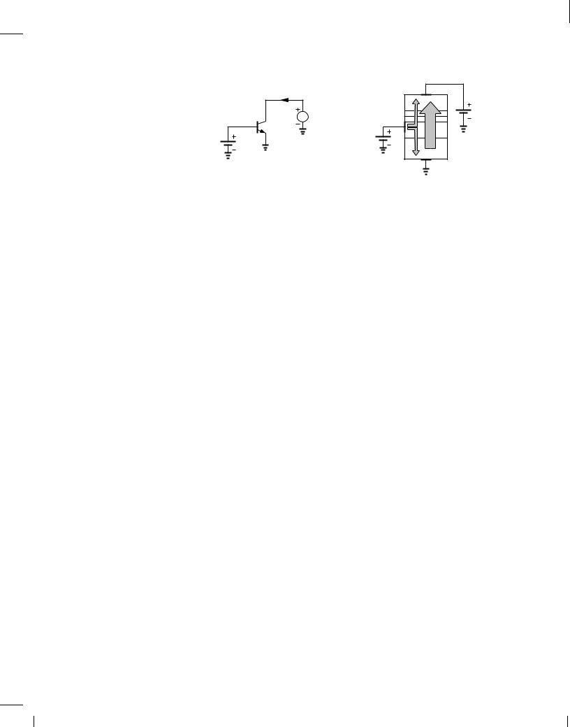
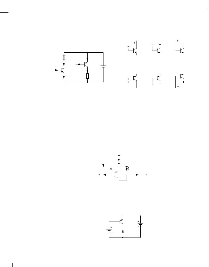
Figure 4.32 Summary of concepts studied thus far.
4.5 Operation of Bipolar Transistor in Saturation Mode
As mentioned in the previous section, it is desirable to operate bipolar devices in the forward active region, where they act as voltage-controlled current sources. In this section, we study the behavior of the device outside this region and the resulting difficulties.
Let us set VBE to a typical value, e.g., 750 mV, and vary the collector voltage from a high level to a low level [Fig. 4.33(a)]. As VCE approaches VBE, and VBC goes from a negative value toward zero, the base-collector junction experiences less reverse bias. For VCE = VBE, the junction sustains a zero voltage difference, but its depletion region still absorbs most of the electrons injected by the emitter into the base. But what happens if VCE < VBE, i.e., VBC > 0 and the B-C junction is forward biased? We say the transistor enters the “saturation region.” Suppose VCE = 550 mV and hence VBC = +200 mV. We know from Chapter 2 that a typical diode sustaining 200 mV of forward bias carries an extremely small current.6 Thus, even in this case the transistor continues to operate as in the active mode, and we say the device is in “soft saturation.”
If the collector voltage drops further, the B-C junction experiences greater forward bias, car-
6About nine orders of magnitude less than one sustaining 750 mV: (750 mV , 200 mV)=(60 mV=dec) 9:2.
BR |
Wiley/Razavi/Fundamentals of Microelectronics [Razavi.cls v. 2006] |
June 30, 2007 at 13:42 |
152 (1) |
|
|
|
|
152 |
Chap. 4 |
Physics of Bipolar Transistors |
I C |
|
n |
|
|
|
VCE |
e− |
VCE |
p |
||
Q 1 |
VBE |
|
VBE |
|
|
h+ |
n + |
|
|
|
|
(a) |
(b) |
|
Figure 4.33 (a) Bipolar transistor with forward-biased base-collector junction, (b) flow of holes to collector.
rying a significant current [Fig. 4.33(b)]. Consequently, a large number of holes must be supplied to the base terminal—as if is reduced. In other words, heavy saturation leads to a sharp rise in the base current and hence a rapid fall in .
Example 4.15
A bipolar transistor is biased with VBE = 750 mV and has a nominal of 100. How much B-C forward bias can the device tolerate if must not degrade by more than 10%? For simplicity, assume base-collector and base-emitter junctions have identical structures and doping levels.
Solution
If the base-collector junction is forward-biased so much that it carries a current equal to onetenth of the nominal base current, IB, then the degrades by 10%. Since IB = IC=100, the B-C junction must carry no more than IC=1000. We therefore ask, what B-C voltage results in a current of IC =1000 if VBE = 750 mV gives a collector current of IC? Assuming identical B-E and B-C junctions, we have
VBE , VBC = VT ln |
IC , VT ln |
IC=1000 |
(4.95) |
|
IS |
IS |
|
= VT ln |
1000 |
|
(4.96) |
180 mV: |
|
(4.97) |
|
That is, VBC = 570 mV:
Exercise
Repeat the above example if VBE = 800 mV.
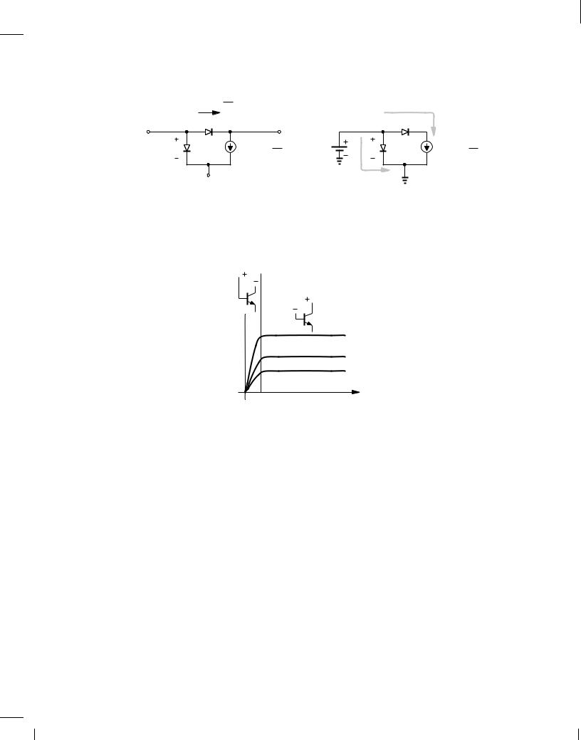
It is instructive to study the transistor large-signal model and I-V characteristics in the saturation region. We construct the model as shown in Fig. 4.34(a), including the base-collector diode. Note that the net collector current decreases as the device enters saturation because part of the controlled current IS1 exp(VBE=VT ) is provided by the B-C diode and need not flow from the collector terminal. In fact, as illustrated in Fig. 4.34(b), if the collector is left open, then DBC is forward-biased so much that its current becomes equal to the controlled current.
The above observations lead to the IC-VCE characteristics depicted in Fig. 4.35, where IC begins to fall for VCE less than V1, about a few hundred millivolts. The term “saturation” is
BR |
Wiley/Razavi/Fundamentals of Microelectronics [Razavi.cls v. 2006] |
June 30, 2007 at 13:42 |
153 (1) |
|
|
|
|
Sec. 4.5 |
Operation of Bipolar Transistor in Saturation Mode |
|
|
|
153 |
||||||
|
|
I S2 exp |
VBE |
|
|
|
|
|
|
|
|
|
|
VT |
|
|
|
|
|
|
|
||
|
|
|
|
|
|
|
|
|
|
|
|
|
B |
|
D BC |
|
C |
|
|
|
|
D BC |
|
|
|
|
|
|
|
|
|
|
|
||
|
V |
D |
|
I S1 exp |
VBE |
V |
|
V |
D |
|
VBE |
|
BE |
|
BE |
BE |
I S1 exp |
||||||
|
BE |
|
|
VT |
|
BE |
|
VT |
|||
|
|
|
|
|
|
|
|
|
|
||
|
|
|
E |
|
|
|
|
|
|
|
|
|
|
|
(a) |
|
|
|
|
|
(b) |
|
|
Figure 4.34 (a) Model of bipolar transistor including saturation effects, (b) case of open collector terminal.
used because increasing the base current in this region of operation leads to little change in the
collector current.
Saturation
Forward
Active Region
I C 
V1 |
VCE |
Figure 4.35 Transistor I/V characteristics in different regions of operation.
In addition to a drop in , the speed of bipolar transistors also degrades in saturation (Chapter 11). Thus, electronic circuits rarely allow operation of bipolar devices in this mode. As a rule of thumb, we permit soft saturation with VBC < 400 mV because the current in the B-C junction is negligible, provided that various tolerances in the component values do not drive the device into deep saturation.
It is important to recognize that the transistor simply draws a current from any component tied to its collector, e.g., a resistor. Thus, it is the external component that defines the collector voltage and hence the region of operation.
Example 4.16 
For the circuit of Fig. 4.36, determine the relationship between RC and VCC that guarantees operation in soft saturation or active region.
Solution
In soft saturation, the collector current is still equal to IS exp(VBE=VT ). The collector voltage must not fall below the base voltage by more than 400 mV:
VCC , RCIC VBE , 400 mV; |
(4.98) |
Thus, |
|
VCC ICRC + (VBE , 400 mV): |
(4.99) |
BR |
Wiley/Razavi/Fundamentals of Microelectronics [Razavi.cls v. 2006] |
June 30, 2007 at 13:42 |
154 (1) |
|
|
|
|
154 |
|
|
|
|
|
|
|
|
|
|
|
|
|
|
|
|
|
|
|
|
|
|
|
|
Chap. 4 |
Physics of Bipolar Transistors |
||
|
|
|
|
|
|
|
|
|
|
|
|
|
|
|
|
|
|
|
|
|
|
|
|
|
|
|
Acceptable |
|
|
|
|
|
|
|
|
|
|
|
R C |
|
|
|
|
|
|
|
|
|
|
|
VCC |
Region |
|||||
|
|
|
|
|
|
|
|
|
|
|
|
|
|
|
|
|
|
|
|
|
|
|||||||
|
|
|
|
|
|
|
|
|
|
I C |
|
|
|
|
|
|
|
|
|
|
|
VCC |
|
|
||||
|
|
|
|
|
|
|
|
|
|
|
|
|
|
|
|
|
|
|
|
|
|
|
||||||
VBE |
|
|
|
|
|
|
|
|
|
|
|
|
|
Q 1 |
|
|
|
|
|
|
|
|
|
VBE − 400 mV |
|
|
||
|
|
|
|
|
|
|
|
|
|
|
|
|
|
|
|
|
|
|
|
|
|
|
|
|
|
|||
|
|
|
|
|
|
|
|
|
|
|
|
|
|
|
|
|
|
|
|
|
|
|
|
|
|
|
R C |
|
|
|
|
|
|
|
|
|
|
|
|
|
|
|
|
|
|
|
|
|
|
|
|
|
|
|
|
||
|
|
|
|
|
|
|
|
|
|
|
|
|
|
|
|
|
|
|
|
|
|
|
|
|
|
|
||
|
|
|
|
|
|
|
|
|
|
|
|
|
|
(a) |
|
|
|
|
|
|
|
|
|
|
|
(b) |
||
Figure 4.36 (a) Simple stage, (b) acceptable range of VCC and RC.
For a given value of RC, VCC must be sufficiently large so that VCC , ICRC still maintains a reasonable collector voltage.
Exercise
Determine the maximum tolerable value of RC.
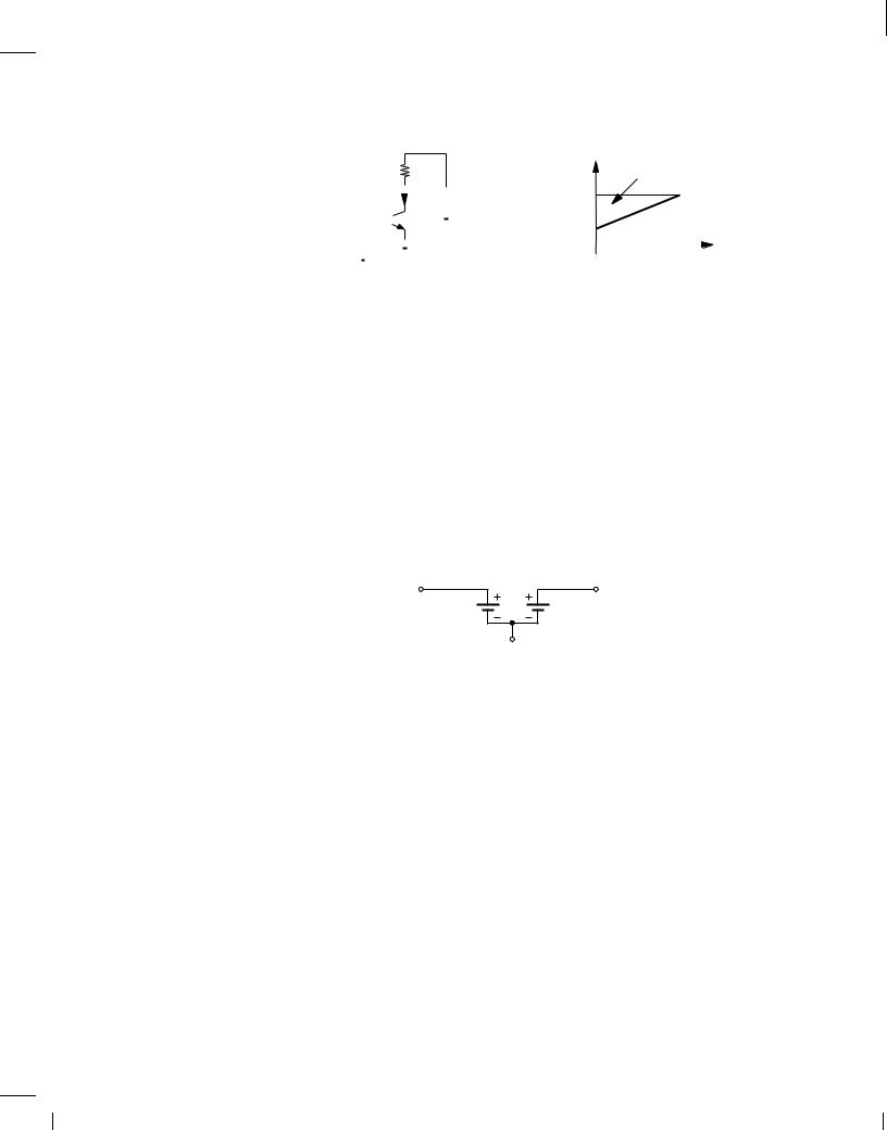
In the deep saturation region, the collector-emitter voltage approaches a constant value called VCE;sat (about 200 mV). Under this condition, the transistor bears no resemblance to a controlled current source and can be modeled as shown in Fig. 4.37. (The battery tied between C and E indicates that VCE is relatively constant in deep saturation.)
B |
C |
800 mV |
200 mV |
E
Figure 4.37 Transistor model in deep saturation.
4.6 The PNP Transistor
We have thus far studied the structure and properties of the npn transistor, i.e., with the emitter and collector made of n-type materials and the base made of a p-type material. We may naturally wonder if the dopant polarities can be inverted in the three regions, forming a “ pnp” device. More importantly, we may wonder why such a device would be useful.
4.6.1 Structure and Operation
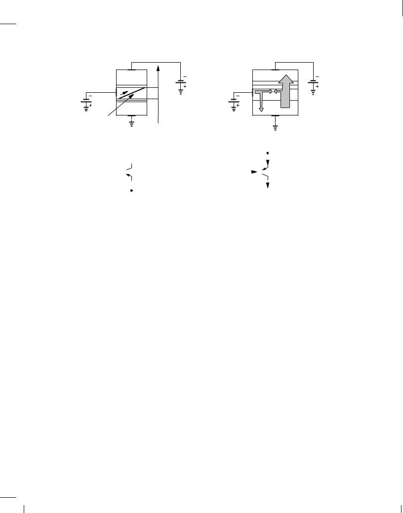
Figure 4.38(a) shows the structure of a pnp transistor, emphasizing that the emitter is heavily doped. As with the npn counterpart, operation in the active region requires forward-biasing the base-emitter junction and reverse-biasing the collector junction. Thus, VBE < 0 and VBC > 0. Under this condition, majority carriers in the emitter (holes) are injected into the base and swept away into the collector. Also, a linear profile of holes is formed in the base region to allow diffusion. A small number of base majority carriers (electrons) are injected into the emitter or recombined with the holes in the base region, thus creating the base current. Figure 4.38(b) illustrates the flow of the carriers. All of the operation principles and equations described for npn transistors apply to pnp devices as well.
BR |
Wiley/Razavi/Fundamentals of Microelectronics [Razavi.cls v. 2006] |
June 30, 2007 at 13:42 |
155 (1) |
|
|
|
|
Sec. 4.6 The PNP Transistor |
155 |
|
p |
x |
|
|
p |
|
|
|
|
||
|
|
x2 |
VCE |
e− |
VCE |
h |
n |
|
n |
||
|
|
|
+ |
|
|
|
|
|
|
|
|
VBE |
|
x1 |
VBE |
h |
|
|
p + |
|
|
e− |
p + |
|
|
|
|
||
Hole |
|
|
|
|
|
Density |
|
|
|
|
|
|
|
|
|
|
|
|
|
|
(a) |
|
|
|
|
|
|
|
|
|
|
|
|
|
|
|
|
(b) |
|
|
|
|
|
|||
|
|
|
|
|
|
|
|
|
|
|
|
|
|
|
|
|
|
|
|
|
|
|
|
|
|
|
|
|
|
|
|
|
|
|
|
|
|
|
|
|
|
|
|
|
|
|
|
|
|
|
|
|
|
|
|
|
|
|
|
|
|
I E |
|
|
|
|
|
||
|
|
|
|
|
|
|
|
|
|
|
|
|
|
|
|
|
VCE |
VBE |
|
|
|
|
|
|
|
|
|
|
|
|
|
|
VCE |
|
VBE |
|
|
|
|
|
|
|
|
Q 1 |
|
|
|
|
|
|
|
|
|
|
|
|
|
|
I B |
|
Q 1 |
|
|
|
|
|
|
||
|
|
|
|
|
|
|
|
|
|
|
|
|
|
|
|
|
|
|
|
|
|
|
|
I C |
|
|
|
|
|
|||||
|
|
|
|
|
|
|
|
|
(c) |
|
|
|
|
|
|
|
|
|
|
|
|
|
|
|
|
|
|
|
|
|
|
|
|
|
|
|
|
|
|
|
|
|
|
|
|
|
|
|
|
|
|
|
|
|
|
|
|
|
|
(d) |
|
|
|
|
|
||||
|
|
|
|
|
|
|
|
|
|
|
|
|
|
|
|
|
|
|
|
|
|
|
|
|
|
|
|
|
|
|
|
|||
Figure 4.38 (a) Structure of pnp transistor, (b) current flow in |
pnp transistor, (c) proper biasing, (d) more |
|||||||||||||||||||||||||||||||||
intuitive view of (c).
Figure 4.38(c) depicts the symbol of the pnp transistor along with constant voltage sources that bias the device in the active region. In contrast to the biasing of the npn transistor in Fig. 4.6, here the base and collector voltages are lower than the emitter voltage. Following our convention of placing more positive nodes on the top of the page, we redraw the circuit as in Fig. 4.38(d) to emphasize VEB > 0 and VBC > 0 and to illustrate the actual direction of current flow into each terminal.
4.6.2 Large-Signal Model
The current and voltage polarities in npn and pnp transistors can be confusing. We address this issue by making the following observations. (1) The (conventional) current always flows from a positive supply (i.e., top of the page) toward a lower potential (i.e., bottom of the page). Figure 4.39(a) shows two branches employing npn and pnp transistors, illustrating that the (conventional) current flows from collector to emitter in npn devices and from emitter to collector in pnp counterparts. Since the base current must be included in the emitter current, we note that IB1 and IC1 add up to IE1 whereas IE2 “loses” IB2 before emerging as IC2. (2) The distinction between active and saturation regions is based on the B-C junction bias. The different cases are summarized in Fig. 4.39(b), where the relative position of the base and collector nodes signifies their potential difference. We note that an npn transistor is in the active mode if the collector (voltage) is not lower than the base (voltage). For the pnp device, on the other hand, the collector must not be higher than the base. (3) The npn current equations (4.23)-(4.25) must be modified as follows for the pnp device
I |
C |
= I |
exp VEB |
|
(4.100) |
|
S |
VT |
|
|
|
|
|
|
|
|
|
I |
|
= IS exp VEB |
|
(4.101) |
|
B |
|
VT |
|
|
|
|
|
|
|
||
IE |
= + 1IS exp |
VEB ; |
(4.102) |
||
|
|
|
|
VT |
|
BR |
Wiley/Razavi/Fundamentals of Microelectronics [Razavi.cls v. 2006] |
June 30, 2007 at 13:42 |
156 (1) |
|
|
|
|
156 |
|
|
Chap. 4 |
Physics of Bipolar Transistors |
|
|
|
|
Active |
Edge of |
Saturation |
|
|
|
Mode |
Saturation |
Mode |
|
|
|
|
0 |
|
|
I E2 |
|
|
|
|
I C1 |
Q 2 |
VCC |
Active |
Edge of |
Saturation |
I B2 |
|
||||
Q 1 |
I C2 |
|
Mode |
Saturation |
Mode |
I B1 |
|
|
|
|
|
I E1 |
|
|
|
|
|
|
|
|
|
0 |
|
|
(a) |
|
|
(b) |
|
Figure 4.39 (a) Voltage and current polarities in npn and pnp transistors, (b) illustration of active and saturation regions.
where the current directions are defined in Fig. 4.40. The only difference between the npn and pnp equations relates to the base-emitter voltage that appears in the exponent, an expected result because VBE < 0 for pnp devices and must be changed to VEB to create a large exponential term. Also, the Early effect can be included as
|
I |
|
= I |
S |
|
exp VEB |
1 + VEC : |
(4.103) |
||||||||||||||
|
C |
|
|
|
|
|
|
|
|
|
|
|
|
VT |
|
VA |
|
|||||
|
|
|
|
|
|
|
|
|
|
|
|
|
|
|
|
|
|
|||||
|
|
|
|
|
|
|
|
|
|
|
|
|
|
|
|
E |
|
|
|
|
|
|
I S |
exp |
VEB |
|
|
|
|
|
|
|
|
|
|
|
I E |
|
|||||||
|
|
|
|
|
|
|
|
|
|
|
|
|||||||||||
β |
|
VT |
|
|
|
|
|
|
|
|
|
|
|
|
|
|
||||||
|
|
|
|
|
|
|
|
|
|
|
|
|
|
|
VEB |
|
||||||
|
|
|
|
|
|
|
|
|
|
|
|
|
|
|
|
|
|
|
|
|||
|
|
|
|
|
|
|
|
|
|
|
|
|
|
|
|
|
|
|
|
|||
|
|
|
|
|
|
V |
|
|
|
|
|
|
|
|
|
|
I S exp |
|
|
|
||
|
|
|
|
|
|
|
|
|
|
|
|
|
|
|||||||||
|
B |
|
|
|
EB |
|
|
|
|
|
|
|
VT |
C |
||||||||
|
|
|
|
|
|
|
|
|
|
|
|
|
|
|
|
|
||||||
|
|
|
|
|
|
|
|
|
|
|
|
|
|
|
|
|
||||||
|
|
I B |
|
|
|
|
|
|
|
|
|
|
I C |
|||||||||
|
|
|
|
|
|
|
|
|
|
|
|
|
|
|
|
|
||||||
|
|
|
|
|
|
|
|
|
|
|
|
|
||||||||||
Figure 4.40 Large-signal model of pnp transistor.
Example 4.17
In the circuit shown in Fig. 4.41, determine the terminal currents of Q1 and verify operation in the forward active region. Assume IS = 2 10,16 A and = 50, but VA = 1.
Q 1 |
VCC |
2 V |
|
X |
|
1.2 V |
Ω |
R C 200 |
Figure 4.41 Simple stage using a pnp transistor.

BR |
Wiley/Razavi/Fundamentals of Microelectronics [Razavi.cls v. 2006] |
June 30, 2007 at 13:42 |
157 (1) |
|
|
|
|
Sec. 4.6 The PNP Transistor |
157 |
Solution
We have VEB = 2 V , 1:2 V = 0:8 V and hence |
|
IC = IS exp VEB |
(4.104) |
VT |
|
= 4:61 mA: |
(4.105) |
It follows that |
|
IB = 92:2 A |
(4.106) |
IE = 4:70 mA: |
(4.107) |
We must now compute the collector voltage and hence the bias across the B-C junction. Since RC carries IC,
VX = RC IC |
(4.108) |
= 0:922 V; |
(4.109) |
which is lower than the base voltage. Invoking the illustration in Fig. 4.39(b), we conclude that Q1 operates in the active mode and the use of equations (4.100)-(4.102) is justified.
Exercise
What is the maximum value of RC is the transistor must remain in soft saturation?
We should mention that some books assume all of the transistor terminal currents flow into the device, thus requiring that the right-hand side of Eqs. (4.100) and (4.101) be multiplied by a negative sign. We nonetheless continue with our notation as it reflects the actual direction of currents and proves more efficient in the analysis of circuits containing many npn and pnp transistors.
Example 4.18
In the circuit of Fig. 4.42, Vin represents a signal generated by a microphone. Determine Vout for Vin = 0 and Vin = +5 mV if IS = 1:5 10,16 A.
|
Q 1 |
|
|
Vin |
I C |
VCC |
2.5 V |
|
Vout |
||
1.7 V |
R C 300 Ω |
|
|
Figure 4.42 PNP stage with bias and small-signal voltages.
Solution
For Vin = 0, VEB = +800 mV and we have
I |
j |
Vin=0 |
= I exp VEB |
(4.110) |
|
|
C |
S |
VT |
|
|
|
|
|
|
|
|
BR |
Wiley/Razavi/Fundamentals of Microelectronics [Razavi.cls v. 2006] |
June 30, 2007 at 13:42 |
158 (1) |
|
|
|
|
158 |
Chap. 4 |
Physics of Bipolar Transistors |
|
= 3:46 mA; |
(4.111) |
|
and hence |
|
|
Vout = 1:038 V: |
(4.112) |
|
If Vin increases to +5 mV, VBE1 = +795 mV and |
|
|
IC jVin=+5 mV = 2:85 mA; |
(4.113) |
|
yielding |
|
|
Vout = 0:856 V: |
(4.114) |
Note that as the base voltage rises, the collector voltage falls, a behavior similar to that of the npn counterparts in Figs. 4.25. Since a 5-mV change in V1 gives a 182-mV change in Vout, the voltage gain is equal to 36.4. These results are more readily obtained through the use of the small-signal model.
Exercise
Determine Vout is Vin = ,5 mV.
4.6.3 Small-Signal Model
Since the small-signal model represents changes in the voltages and currents, we expect npn and pnp transistors to have similar models. Depicted in Fig. 4.43(a), the small-signal model of the pnp transistor is indeed identical to that of the npn device. Following the convention in Fig. 4.38(d), we sometimes draw the model as shown in Fig. 4.43(b).
i b |
i c |
|
|
E |
|
|
i e |
||
B |
|
C |
|
|
r π vπ |
gm vπ r O |
r |
π vπ |
gm vπ r O |
|
|
|||
i e |
|
B |
|
C |
E |
|
i b |
|
i c |
|
|
|
(b) |
|
(a) |
|
|
|
|
|
|
|
|
Figure 4.43 (a) Small-signal model of pnp transistor, (b) more intuitive view of (a).
The reader may notice that the terminal currents in the small-signal model bear an opposite direction with respect to those in the large-signal model of Fig. 4.40. This is not an inconsistency and is studied in Problem 49.
The small-signal model of pnp transistors may cause confusion, especially if drawn as in Fig. 4.43(b). In analogy with npn transistors, one may automatically assume that the “top” terminal is the collector and hence the model in Fig. 4.43(b) is not identical to that in Fig. 4.31(b). We caution the reader about this confusion. A few examples prove helpful here.
BR |
Wiley/Razavi/Fundamentals of Microelectronics [Razavi.cls v. 2006] |
June 30, 2007 at 13:42 |
159 (1) |
|
|
|
|
Sec. 4.6 The PNP Transistor |
159 |
Example 4.19
If the collector and base of a bipolar transistor are tied together, a two-terminal device results. Determine the small-signal impedance of the devices shown in Fig. 4.44(a). Assume VA = 1.
|
|
i X |
|
|
Q 2 |
r π vπ |
gmvπ |
Q 1 |
v X |
||
(a) |
|
(b) |
|
Figure 4.44
Solution
We replace the bipolar transistor Q1 with its small-signal model and apply a small-signal voltage across the device [Fig. 4.44(b)]. Noting that rpi carries a current equal to vX =r , we write a KCL at the input node:
vX + gmv = iX : |
(4.115) |
||||
r |
|
|
|
|
|
Since gmr = 1, we have |
|
|
|
|
|
vX = |
|
1 |
|
(4.116) |
|
gm |
+ r 1 |
||||
iX |
|
||||
|
|
, |
|
|
|
|
1 |
|
|
(4.117) |
|
gm |
|
|
|||
|
|
|
|
||
= |
VT : |
(4.118) |
|||
|
IC |
|
|
|
|
Interestingly, with a bias current of IC, the device exhibits an impedance similar to that of a diode carrying the same bias current. We call this structure a “diode-connected transistor.” The same results apply to the pnp configuration in Fig. 4.44(a).
Exercise
What is the impedance of a diode-connected device operating at a current of 1 mA?
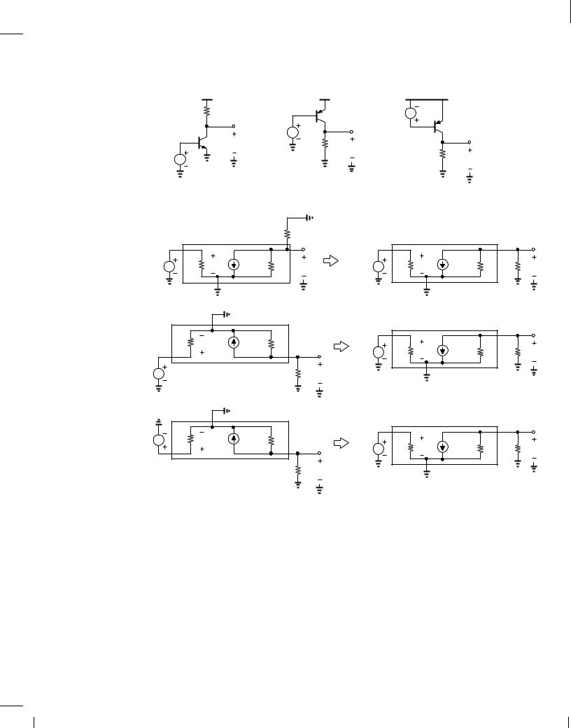
Example 4.20
Draw the small-signal equivalent circuits for the topologies shown in Figs. 4.45(a)-(c) and compare the results.
Solution
As illustrated in Figs. 4.45(d)-f, we replace each transistor with its small-signal model and ground the supply voltage. It is seen that all three topologies reduce to the same equivalent circuit because VCC is grounded in the small-signal representation.
BR |
Wiley/Razavi/Fundamentals of Microelectronics [Razavi.cls v. 2006] |
June 30, 2007 at 13:42 |
160 (1) |
|
|
|
|
160 |
|
Chap. 4 |
Physics of Bipolar Transistors |
|
VCC |
|
VCC |
|
VCC |
R C |
|
Q 1 |
v in |
|
|
|
|
Q 1 |
|
|
v in |
|
|
|
Q 1 v out |
|
|
|
|
R C |
v out |
R C |
|
|
v in |
|
v out |
||
|
|
|||
|
|
|
||
(a) |
|
(b) |
|
(c) |
|
|
|
|
R C |
|
|
v in |
r π |
vπ |
gm vπ |
r O |
v out |
v in |
r π |
vπ |
gm vπ |
r O R C |
v out |
|
|
|
|
|
(d) |
|
|
|
|
|
|
|
r π |
vπ |
gmvπ |
r O |
v in |
r π |
vπ |
gm vπ |
r O |
R C |
v out |
|
|
|
|
|
|||||||
v in |
|
|
|
R C |
v out |
|
|
|
|
|
|
|
|
|
|
|
(e) |
|
|
|
|
|
|
v in |
r π |
vπ |
gmvπ |
r O |
v in |
r π |
vπ |
gm vπ |
r O |
R C |
v out |
|
|
|
|
|
|||||||
|
|
|
|
R C |
v out |
|
|
|
|
|
|
(f)
Figure 4.45 (a) Simple stage using an npn transistor, (b) simple stage using a pnp transistor, (c) another pnp stage, (d) small-signal equivalent of (a), (e) small-signal equivalent of (b), (f) small-signal equivalent of (f).
Exercise
Repeat the above example if a resistor is placed between the collector and base of each transistor.
Example 4.21 
Draw the small-signal equivalent circuit for the amplifier shown in Fig. 4.46(a).