

Fundamentals of Microelectronics
.pdfBR |
Wiley/Razavi/Fundamentals of Microelectronics [Razavi.cls v. 2006] |
June 30, 2007 at 13:42 |
41 (1) |
|
|
|
|
Sec. 2.2 |
P N Junction |
41 |
Example 2.14
Equation (2.69) reveals that V0 is a weak function of the doping levels. How much does V0 change if NA or ND is increased by one order of magnitude?
Solution
We can write
V |
= V ln 10NA |
ND |
, V |
ln NA ND |
(2.72) |
|
0 |
T |
n2 |
T |
n2 |
|
|
|
|
|
|
|||
|
|
|
i |
|
i |
|
|
= VT ln 10 |
|
|
|
|
(2.73) |
|
60 mV (at T = 300 K): |
|
(2.74) |
|||
Exercise
How much does V0 change if NA or ND is increased by a factor of three?
An interesting question may arise at this point. The junction carries no net current (because its terminals remain open), but it sustains a voltage. How is that possible? We observe that the builtin potential is developed to oppose the flow of diffusion currents (and is, in fact, sometimes called the “potential barrier.”). This phenomenon is in contrast to the behavior of a uniform conducting material, which exhibits no tendency for diffusion and hence no need to create a built-in voltage.
2.2.2 P N Junction Under Reverse Bias
Having analyzed the pn junction in equilibrium, we can now study its behavior under more interesting and useful conditions. Let us begin by applying an external voltage across the device as shown in Fig. 2.23, where the voltage source makes the n side more positive than the p side. We say the junction is under “reverse bias” to emphasize the connection of the positive voltage to the n terminal. Used as a noun or a verb, the term “bias” indicates operation under some “desirable” conditions. We will study the concept of biasing extensively in this and following chapters.
We wish to reexamine the results obtained in equilibrium for the case of reverse bias. Let
us first determine whether the external voltage enhances the built-in electric field or opposes it.
!
Since under equilibrium, E is directed from the n side to the p side, VR enhances the field. But, a higher electric field can be sustained only if a larger amount of fixed charge is provided, requiring that more acceptor and donor ions be exposed and, therefore, the depletion region be widened.
What happens to the diffusion and drift currents? Since the external voltage has strengthened the field, the barrier rises even higher than that in equilibrium, thus prohibiting the flow of current. In other words, the junction carries a negligible current under reverse bias.9
With no current conduction, a reverse-biased pn junction does not seem particularly useful. However, an important observation will prove otherwise. We note that in Fig. 2.23, as VB increases, more positive charge appears on the n side and more negative charge on the p side.
9As explained in Section 2.2.3, the current is not exactly zero.
BR |
Wiley/Razavi/Fundamentals of Microelectronics [Razavi.cls v. 2006] |
June 30, 2007 at 13:42 |
42 (1) |
|
|
|
|
42 |
|
|
|
|
|
Chap. 2 |
|
|
Basic Physics of Semiconductors |
|||||
|
|
|
|
n |
|
|
|
|
|
|
p |
|
|
|
|
− |
|
− |
|
− |
+ + |
− |
−+ |
|
+ |
|
+ |
|
|
− |
− |
− |
− |
− |
− + + − − + |
+ |
+ |
+ |
+ |
+ |
||||
− |
− |
− |
− |
− |
− |
+ + − − + |
+ |
+ |
+ |
+ |
+ |
|||
− |
− |
− |
− |
− |
− |
+ + − − |
+ |
+ |
+ |
+ |
+ |
+ |
||
− |
|
− |
|
− |
|
+ + |
− |
− |
|
+ |
|
+ |
|
+ |
|
|
|
|
n |
|
|
|
|
|
|
p |
|
|
|
|
− |
|
− |
|
|
+ + + |
− |
− |
− |
+ |
+ |
|
||
− |
− |
− |
− |
|
|
+ + + − − − + |
+ |
+ |
+ |
|||||
− |
− |
− |
− |
|
|
+ + + |
− |
− |
− |
|
+ |
+ |
+ |
+ |
− |
− |
|
|
|
+ |
+ |
||||||||
|
|
+ + + − − − |
|
|||||||||||
− |
− |
− |
− |
|
|
+ + + − − − |
|
+ |
+ |
+ |
+ |
|||
VR
Figure 2.23 PN junction under reverse bias.
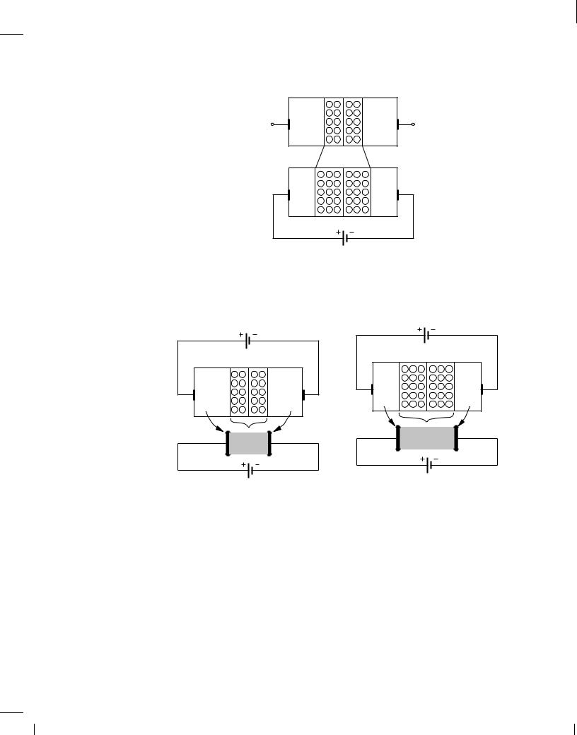
Thus, the device operates as a capacitor [Fig. 2.24(a)]. In essence, we can view the conductive n and p sections as the two plates of the capacitor. We also assume the charge in the depletion region equivalently resides on each plate.
|
|
|
|
n |
|
VR1 |
|
|
|
p |
|
|
|
|
|
|
|
|
|
|
|
|
|
|
|
||
|
− |
|
− |
|
− |
+ + − |
−+ |
|
+ |
|
+ |
|
|
− |
− |
− |
− |
− |
− + + − − + |
+ |
+ |
+ |
+ |
+ |
|||
− |
− |
− |
− |
− |
− |
+ + − − + |
+ |
+ |
+ |
+ |
+ |
||
− |
− |
− |
− |
− |
− |
+ + − − |
+ |
+ |
+ |
+ |
+ |
+ |
|
− |
|
− |
|
− |
|
+ + − |
− |
|
+ |
|
+ |
|
+ |
|
|
|
|
|
− |
|
|
+ |
|
|
|
|
|
|
|
|
|
|
− |
|
|
+ |
|
|
|
|
|
|
|
|
|
|
− |
|
|
+ |
|
|
|
|
|
|
|
|
|
|
− |
|
|
+ |
|
|
|
|
|
VR1
|
|
|
n |
|
VR2 |
p |
|
|
|
|
|
|
|
|
|
|
|
||
|
− |
|
− |
|
+ + + − − − |
+ |
+ |
|
|
− |
− |
− |
− |
|
+ + + − − − + |
+ |
+ |
+ |
|
− |
− |
− |
− |
|
+ + + − − − |
+ |
+ |
+ |
+ |
− |
− |
|
+ |
+ |
|||||
|
+ + + − − − |
||||||||
− |
− |
− |
− |
|
+ + + − − − |
+ |
+ |
+ |
+ |
|
|
|
− |
− |
|
+ |
|
|
|
|
|
|
− |
|
|
+ |
|
|
|
|
|
|
− |
|
|
+ |
|
|
|
|
|
|
− |
|
|
+ |
|
|
|
VR2 (more negative than VR1 )
(a) |
(b) |
Figure 2.24 Reduction of junction capacitance with reverse bias.
The reader may still not find the device interesting. After all, since any two parallel plates can form a capacitor, the use of a pn junction for this purpose is not justified. But, reverse-biased pn junctions exhibit a unique property that becomes useful in circuit design. Returning to Fig. 2.23, we recognize that, as VR increases, so does the width of the depletion region. That is, the conceptual diagram of Fig. 2.24(a) can be drawn as in Fig. 2.24(b) for increasing values of VR, revealing that the capacitance of the structure decreases as the two plates move away from each other. The junction therefore displays a voltage-dependent capacitance.
It can be proved that the capacitance of the junction per unit area is equal to
Cj = |
|
Cj0 |
|
; |
(2.75) |
|
|
|
|||
|
r1 , |
VR |
|
||
|
V0 |
|
|||
BR |
Wiley/Razavi/Fundamentals of Microelectronics [Razavi.cls v. 2006] |
June 30, 2007 at 13:42 |
43 (1) |
|
|
|
|
Sec. 2.2 |
P N Junction |
43 |
where Cj0 denotes the capacitance corresponding to zero bias (VR = 0) and V0 is the built-in potential [Eq. (2.69)]. (This equation assumes VR is negative for reverse bias.) The value of Cj0 is in turn given by
Cj0 |
= r |
siq |
NAND |
|
1 |
|
; |
|
|
||||||
|
|
2 NA + ND V0 |
|||||
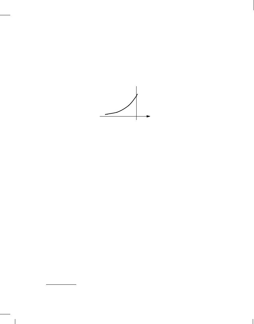
where si represents the dielectric constant of silicon and is equal to 11:7 Plotted in Fig. 2.25, Cj indeed decreases as VR increases.
(2.76)
8:85 10,14 F/cm.10
 Cj
Cj
0 VR
Figure 2.25 Junction capacitance under reverse bias.
Example 2.15
A pn junction is doped with NA = 2 1016 cm,3 and ND = 9 1015 cm,3. Determine the capacitance of the device with (a) VR = 0 and VR = 1 V.
Solution
We first obtain the built-in potential:
|
V |
= V |
ln NAND |
|
|
|
|
|
0 |
|
T |
n2 |
|
|
|
|
|
|
|
|
|
|
|
|
|
|
|
i |
|
|
|
|
|
= 0:73 V: |
|
|
|
||
Thus, for VR = 0 and q = 1:6 10,19 C, we have |
|
|
|
||||
|
|
|
|
|
|
||
C |
= r siq |
NAND |
|
1 |
|
||
|
|
||||||
j0 |
|
2 |
NA + ND |
|
V0 |
||
|
|
|
|||||
= 2:65 10,8 F=cm2:
In microelectronics, we deal with very small devices and may rewrite this result as
Cj0 = 0:265 fF= m2;
where 1 fF (femtofarad) = 10,15 F. For VR = 1 V,
Cj = |
|
Cj0 |
|
|
|
|
|
|
|
||
r1 + |
VR |
||||
|
|||||
|
V0 |
||||
= |
0:172 fF= m2: |
||||
(2.77)
(2.78)
(2.79)
(2.80)
(2.81)
(2.82)
(2.83)
10The dielectric constant of materials is usually written in the form r 0, where r is the “relative” dielectric constant and a dimensionless factor (e.g., 11.7), and 0 the dielectric constant of vacuum (8:85 10,14 F/cm).
BR |
Wiley/Razavi/Fundamentals of Microelectronics [Razavi.cls v. 2006] |
June 30, 2007 at 13:42 |
44 (1) |
|
|
|
|
44 |
Chap. 2 |
Basic Physics of Semiconductors |
Exercise
Repeat the above example if the donor concentration on the N side is doubled. Compare the results in the two cases.
The variation of the capacitance with the applied voltage makes the device a “nonlinear” capacitor because it does not satisfy Q = CV . Nonetheless, as demonstrated by the following example, a voltage-dependent capacitor leads to interesting circuit topologies.
Example 2.16
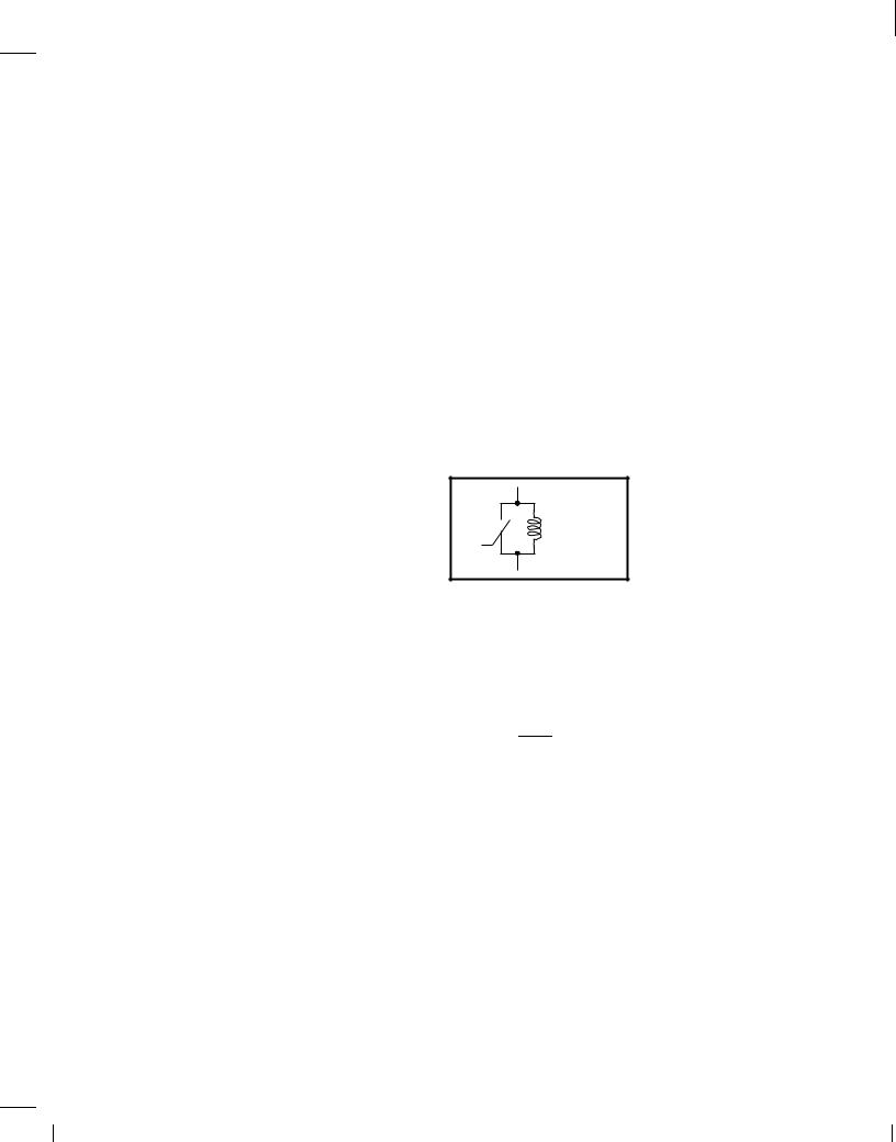
A cellphone incorporates a 2-GHz oscillator whose frequency is defined by the resonance frequency of an LC tank (Fig. 2.26). If the tank capacitance is realized as the pn junction of Example 2.15, calculate the change in the oscillation frequency while the reverse voltage goes from 0 to 2 V. Assume the circuit operates at 2 GHz at a reverse voltage of 0 V, and the junction area is 2000 m2.
Oscillator
C  L
L
VR
Figure 2.26 Variable capacitor used to tune an oscillator.
Solution
Recall from basic circuit theory that the tank “resonates” if the impedances of the inductor and the capacitor are equal and opposite: jL!res = ,(jC!res),1. Thus, the resonance frequency is equal to
fres = |
1 |
|
p |
1 |
: |
|
|
(2.84) |
|||
|
2 |
|
|||||||||
|
|
|
|
|
|||||||
|
|
|
|
LC |
|
|
|||||
At VR = 0, Cj = 0:265 fF/ m2, yielding a total device capacitance of |
|
||||||||||
Cj;tot(VR = 0) = (0:265 fF= m2) (2000 m2) |
(2.85) |
||||||||||
= 530 fF: |
|
|
|
|
|
|
|
(2.86) |
|||
Setting fres to 2 GHz, we obtain |
|
|
|
|
|
|
|
|
|
|
|
L = 11:9 nH: |
|
(2.87) |
|||||||||
If VR goes to 2 V, |
|
|
|
|
|
|
|
|
|
|
|
Cj;tot(VR = 2 V) = |
|
|
|
Cj0 |
2000 m2 |
(2.88) |
|||||
|
|
|
|
|
|
|
|
|
|||
|
|
|
2 |
|
|||||||
|
|
|
|
|
|
|
|||||
|
r1 + |
|
|
|
|
||||||
|
0:73 |
|
(2.89) |
||||||||
= 274 fF: |
|
||||||||||
BR |
Wiley/Razavi/Fundamentals of Microelectronics [Razavi.cls v. 2006] |
June 30, 2007 at 13:42 |
45 (1) |
|
|
|
|
Sec. 2.2 P N Junction |
45 |
Using this value along with L = 11:9 nH in Eq. (2.84), we have |
|
fres(VR = 2 V) = 2:79 GHz: |
(2.90) |
An oscillator whose frequency can be varied by an external voltage (VR in this case) is called a “voltage-controlled oscillator” and used extensively in cellphones, microprocessors, personal computers, etc.
Exercise
Some wireless systems operate at 5.2 GHz. Repeat the above example for this frequency, assuming the junction area is still 2000 m2 but the inductor value is scaled to reach 5.2 GHz.
In summary, a reverse-biased pn junction carries a negligible current but exhibits a voltagedependent capacitance. Note that we have tacitly developed a circuit model for the device under this condition: a simple capacitance whose value is given by Eq. (2.75).
Another interesting application of reverse-biased diodes is in digital cameras (Chapter 1). If light of sufficient energy is applied to a pn junction, electrons are dislodged from their covalent bonds and hence electron-hole pairs are created. With a reverse bias, the electrons are attracted to the positive battery terminal and the holes to the negative battery terminal. As a result, a current flows through the diode that is proportional to the light intensity. We say the pn junction operates as a “photodiode.”
2.2.3 P N Junction Under Forward Bias
Our objective in this section is to show that the pn junction carries a current if the p side is raised to a more positive voltage than the n side (Fig. 2.27). This condition is called “forward bias.” We also wish to compute the resulting current in terms of the applied voltage and the junction parameters, ultimately arriving at a circuit model.
|
|
|
|
|
n |
|
|
|
|
|
|
|
|
|
|
|
p |
|
|
|
|
|
|
|
|
|
|
|
|
|
|
|
|
|
|
|
|
|
|
|
|
|
|
|
|
|
|
|
|
− |
|
− |
|
− |
|
+ |
|
|
− |
+ |
|
+ |
|
+ |
|
|
|
||||
|
− |
− |
− |
− |
− |
− |
− |
+ − |
+ |
+ |
+ |
+ |
+ |
+ |
+ |
|
|||||||
|
− |
− |
− |
− |
− |
− |
− |
+ |
|
|
− |
+ |
+ |
+ |
+ |
+ |
+ |
+ |
|
||||
|
|
|
|
||||||||||||||||||||
|
− |
− |
− |
− |
+ − |
+ |
+ |
+ |
+ |
|
|||||||||||||
|
− |
− |
− |
+ |
+ |
+ |
|
||||||||||||||||
|
− |
− |
− |
− + − + |
+ |
+ |
+ |
|
|||||||||||||||
|
|
|
|
|
|
|
|
|
|
|
|
|
|
|
|
|
|
|
|
|
|
|
|
|
|
|
|
|
|
|
|
|
|
|
|
|
|
|
|
|
|
|
|
|
|
|
|
|
|
|
|
|
|
|
|
|
|
|
|
|
|
|
|
|
|
|
|
|
|
|
|
|
|
|
|
|
|
|
|
|
|
|
|
|
|
|
|
|
|
|
|
|
|
|
|
VF
Figure 2.27 PN junction under forward bias.
From our study of the device in equilibrium and reverse bias, we note that the potential barrier developed in the depletion region determines the device's desire to conduct. In forward bias, the external voltage, VF , tends to create a field directed from the p side toward the n side—opposite to the built-in field that was developed to stop the diffusion currents. We therefore surmise that VF in fact lowers the potential barrier by weakening the field, thus allowing greater diffusion currents.
BR |
Wiley/Razavi/Fundamentals of Microelectronics [Razavi.cls v. 2006] |
June 30, 2007 at 13:42 |
46 (1) |
|
|
|
|
46 |
Chap. 2 |
Basic Physics of Semiconductors |
To derive the I/V characteristic in forward bias, we begin with Eq. (2.68) for the built-in voltage and rewrite it as
p = |
pp;e |
; |
(2.91) |
||
|
|
||||
n;e |
V0 |
|
|
|
|
|
exp |
|
|
||
|
VT |
|
|
||
|
|
|
|
||
where the subscript e emphasizes equilibrium conditions [Fig. 2.28(a)] and VT = kT=q is called
|
n |
p |
n |
n,e |
pp,e |
|
|
|
p |
n,e |
np,e |
|
|
|
n |
p |
n |
n,f |
pp,f |
|
|
|
p |
n,f |
np,f |
|
|
|
|
pn,e |
np,f |
VF
(a) |
(b) |
Figure 2.28 Carrier profiles (a) in equilibrium and (b) under forward bias.
the “thermal voltage” ( 26 mV at T = 300 K). In forward bias, the potential barrier is lowered by an amount equal to the applied voltage:
pn;f = |
|
pp;f |
: |
(2.92) |
|
exp |
V0 , VF |
||||
|
|
|
|||
|
|
VT |
|
|
where the subscript f denotes forward bias. Since the exponential denominator drops considerably, we expect pn;f to be much higher than pn;e (it can be proved that pp;f pp;e NA). In other words, the minority carrier concentration on the p side rises rapidly with the forward bias voltage while the majority carrier concentration remains relatively constant. This statement applies to the n side as well.
Figure 2.28(b) illustrates the results of our analysis thus far. As the junction goes from equilibrium to forward bias, np and pn increase dramatically, leading to a proportional change in the diffusion currents.11 We can express the change in the hole concentration on the n side as:
pn = pn;f , pn;e |
|
|
|
|
(2.93) |
|||
= |
|
pp;f |
, |
pp;e |
(2.94) |
|||
exp |
V0 , VF |
exp |
V0 |
|
||||
|
|
|
|
|||||
|
|
VT |
|
|||||
|
|
VT |
|
|
|
|||
|
NA |
(exp |
VF , 1): |
(2.95) |
||||
|
||||||||
|
exp |
V0 |
VT |
|
||||
|
VT |
|
|
|
|
|
||
Similarly, for the electron concentration on the p side:
np |
ND |
(exp |
VF |
, 1): |
(2.96) |
||
exp |
V0 |
VT |
|||||
|
|
|
|
||||
|
VT |
|
|
|
|
||
11The width of the depletion region actually decreases in forward bias but we neglect this effect here.

BR |
Wiley/Razavi/Fundamentals of Microelectronics [Razavi.cls v. 2006] |
June 30, 2007 at 13:42 |
47 (1) |
|
|
|
|
Sec. 2.2 P N Junction 47
Note that Eq. (2.69) indicates that exp(V0=VT ) = NAND=n2.
i
The increase in the minority carrier concentration suggests that the diffusion currents must rise by a proportional amount above their equilibrium value, i.e.,
I / |
NA |
(exp VF |
, 1) + |
|
ND |
(exp VF , 1): |
(2.97) |
||||
|
|
|
|
|
|||||||
tot |
V0 |
VT |
|
|
|
|
V0 |
VT |
|
||
|
exp |
|
|
exp |
|
||||||
|
VT |
|
|
|
VT |
|
|
|
|||
Indeed, it can be proved that [1] |
|
|
|
|
|
|
|
|
|
||
|
|
|
I = I |
S |
(exp VF |
, 1); |
|
|
(2.98) |
||
|
|
|
tot |
VT |
|
|
|
|
|
||
|
|
|
|
|
|
|
|
|
|
||
where IS is called the “reverse saturation current” and given by
I |
S |
= Aqn2( |
Dn |
+ |
Dp |
): |
(2.99) |
|
|
||||||
|
i |
NALn |
|
NDLp |
|
||
In this equation, A is the cross section area of the device, and Ln and Lp are electron and hole “diffusion lengths,” respectively. Diffusion lengths are typically in the range of tens of micrometers. Note that the first and second terms in the parentheses correspond to the flow of electrons and holes, respectively.
Example 2.17
Determine IS for the junction of Example 2.13 at T = 300K if A = 100 m2, Ln = 20 m, and Lp = 30 m.
Solution
Using q = 1:6 10,19 C, ni = 1:08 1010 electrons=cm3 [Eq. (2.2)], Dn = 34 cm2=s, and
Dp = 12 cm2=s, we have
IS = 1:77 10,17 A: |
(2.100) |
Since IS is extremely small, the exponential term in Eq. (2.98) must assume very large values so as to yield a useful amount (e.g., 1 mA) for Itot.
Exercise
What junction area is necessary to raise IS to 10,15 A.
An interesting question that arises here is: are the minority carrier concentrations constant along the x-axis? Depicted in Fig. 2.29(a), such a scenario would suggest that electrons continue to flow from the n side to the p side, but exhibit no tendency to go beyond x = x2 because of the lack of a gradient. A similar situation exists for holes, implying that the charge carriers do not flow deep into the p and n sides and hence no net current results! Thus, the minority carrier concentrations must vary as shown in Fig. 2.29(b) so that diffusion can occur.
This observation reminds us of Example 2.10 and the question raised in conjunction with it: if the minority carrier concentration falls with x, what happens to the carriers and how can the current remain constant along the x-axis? Interestingly, as the electrons enter the p side and roll down the gradient, they gradually recombine with the holes, which are abundant in this region.
BR |
Wiley/Razavi/Fundamentals of Microelectronics [Razavi.cls v. 2006] |
June 30, 2007 at 13:42 |
48 (1) |
|
|
|
|
48 |
|
|
|
|
|
|
|
|
|
|
|
|
Chap. 2 |
Basic Physics of Semiconductors |
||||||||||||||
|
|
Electron |
|
|
|
|
|
|
Hole |
|
|
Electron |
|
|
|
|
|
|
|
|
Hole |
|||||||
|
|
n |
Flow |
|
|
|
|
|
|
Flow |
|
|
Flow |
|
|
|
|
|
|
|
|
|
Flow |
|||||
|
|
|
|
|
|
|
|
|
p |
|
|
n |
|
|
|
|
|
|
|
|
|
p |
||||||
|
|
|
|
|
|
|
|
|
|
|
|
|
|
|
|
|||||||||||||
|
|
nn,f |
− − ++ |
pp,f |
|
|
|
|
nn,f |
|
− − ++ |
|
pp,f |
|
|
|
||||||||||||
|
|
|
|
+ − |
|
|
|
|
|
|
|
|
|
+ |
|
|
− |
|
|
|
|
|
||||||
|
|
|
|
|
|
|
|
|
|
|
|
|
|
|
|
|
|
|
|
|||||||||
|
|
pn,f |
+ |
|
|
|
|
− |
np,f |
|
|
|
|
pn,f+ + + |
+ |
|
|
|
|
|
|
− |
− |
np,f |
|
|
|
|
|
|
|
|
|
|
|
|
|
|
|
|
|
|
|
|
|
|
|
||||||||||
|
|
|
|
|
|
|
|
|
|
|
|
|
|
|
|
|
|
|
|
|
− − |
|
|
|
||||
|
|
|
|
|
|
|
|
|
|
|
|
|
|
|
|
|
|
|||||||||||
|
|
|
x 1 x 2 |
|
x |
|
|
x 1 |
|
|
x 2 |
|
|
x |
|
|||||||||||||
|
|
|
|
|
|
|
|
|
|
|
|
|
|
|
|
|
|
|
|
|
|
|
|
|
|
|
|
|
|
|
|
|
|
|
|
|
|
|
|
|
|
|
|
|
|
|
|
|
|
|
|
|
|
|
|
|
|
|
|
|
|
|
|
|
|
|
|
|
|
|
|
|
|
|
|
|
|
|
|
|
|
|
|
|
|
|
|
|
|
|
V |
|
|
|
|
|
|
|
|
|
|
|
V |
|
|
|
|
|
|
|
|
||||
|
|
|
|
F |
|
|
|
|
|
|
|
|
|
F |
|
|
|
|
|
|||||||||
|
|
|
|
(a) |
|
|
|
|
|
|
|
|
|
|
|
|
(b) |
|
|
|
|
|
||||||
Figure 2.29 (a) Constant and (b) variable majority carrier profiles ioutside the depletion region.
Similarly, the holes entering the n side recombine with the electrons. Thus, in the immediate vicinity of the depletion region, the current consists of mostly minority carriers, but towards the far contacts, it is primarily comprised of majority carriers (Fig. 2.30). At each point along the x-axis, the two components add up to Itot.
|
|
n |
|
|
|
|
p |
|
|
− |
− |
|
|
|
|
|
|
+ + |
|
− |
− |
|
|
|
|
+ |
|||
− |
− |
|
|
+ |
+ |
+ |
|||
− |
− |
|
|
||||||
− |
|
|
|
+ |
+ |
||||
− |
+ |
+ |
+ |
− |
− |
|
+ + |
||
|
− |
||||||||
|
|
+ |
− |
|
|
||||
|
+ |
+ |
+ |
+ |
− |
− |
− |
− |
|
|
|
|
+ |
+ |
− |
− |
|
|
|
|
|
|
|
|
|
|
|
|
x |
VF
Figure 2.30 Minority and majority carrier currents.
2.2.4 I/V Characteristics
Let us summarize our thoughts thus far. In forward bias, the external voltage opposes the built-in potential, raising the diffusion currents substantially. In reverse bias, on the other hand, the applied voltage enhances the field, prohibiting current flow. We hereafter write the junction equation as:
ID = IS(exp |
VD , 1); |
(2.101) |
|
VT |
|
where ID and VD denote the diode current and voltage, respectively. As expected, VD = 0 yields ID = 0. (Why is this expected?) As VD becomes positive and exceeds several VT , the exponential term grows rapidly and ID IS exp(VD=VT ). We hereafter assume exp(VD=VT ) 1 in the forward bias region.
It can be proved that Eq. (2.101) also holds in reverse bias, i.e., for negative VD. If VD < 0 and jVDj reaches several VT , then exp(VD=VT ) 1 and
ID ,IS: |
(2.102) |
BR |
Wiley/Razavi/Fundamentals of Microelectronics [Razavi.cls v. 2006] |
June 30, 2007 at 13:42 |
49 (1) |
|
|
|
|
Sec. 2.2 P N Junction 49
Figure 2.31 plots the overall I/V characteristic of the junction, revealing why IS is called the
“reverse saturation current.” Example 2.17 indicates that |
IS is typically very small. We therefore |
||
|
Reverse |
Forward |
|
|
Bias |
Bias |
|
|
|
|
|
|
I D |
|
|
 I S exp VD
VT
− I S |
VD |
|
Figure 2.31 I-V characteristic of a pn junction.
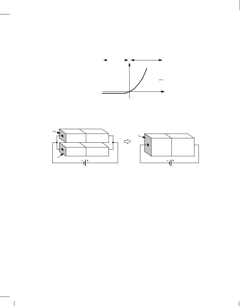
view the current under reverse bias as “leakage.” Note that IS and hence the junction current are proportional to the device cross section area [Eq. (2.99)]. For example, two identical devices placed in parallel (Fig. 2.32) behave as a single junction with twice the IS.
A
n |
2A |
|
p |
|
|
|
n |
p |
n |
p |
|
A |
|
|
VF |
|
VF |
Figure 2.32 Equivalence of parallel devices to a larger device.
Example 2.18
Each junction in Fig. 2.32 employs the doping levels described in Example 2.13. Determine the forward bias current of the composite device for VD = 300 mV and 800 mV at T = 300 K.
Solution
From Example 2.17, IS = 1:77 10,17 A for each junction. Thus, the total current is equal to
I |
(V |
= 300 mV) = 2I |
S |
(exp VD |
, 1) |
(2.103) |
D;tot |
D |
|
VT |
|
|
|
|
|
|
|
|
|
|
|
|
= 3:63 pA: |
|
(2.104) |
||
Similarly, for VD = 800 mV: |
|
|
|
|
|
|
ID;tot(VD = 800 mV) = 82 A: |
|
(2.105) |
||||
Exercise
How many of these diodes must be placed in parallel to obtain a current of 100 A with a

BR |
Wiley/Razavi/Fundamentals of Microelectronics [Razavi.cls v. 2006] |
June 30, 2007 at 13:42 |
50 (1) |
|
|
|
|
50 |
Chap. 2 |
Basic Physics of Semiconductors |
voltage of 750 mV.
Example 2.19
A |
diode operates in the forward bias region with a typical current level [i.e., |
ID |
IS exp(VD=VT )]. Suppose we wish to increase the current by a factor of 10. How |
much change in VD is required?
Solution
Let us first express the diode voltage as a function of its current:
VD = VT ln ID :
IS
We define I1 = 10ID and seek the corresponding voltage, VD1:
VD1 = VT ln 10ID
IS
= VT ln ID + VT ln 10
IS
= VD + VT ln 10:
(2.106)
(2.107)
(2.108)
(2.109)
Thus, the diode voltage must rise by VT ln 10 60 mV (at T = 300 K) to accommodate a tenfold increase in the current. We say the device exhibits a 60-mV/decade characteristic, meaning VD changes by 60 mV for a decade (tenfold) change in ID. More generally, an n-fold change in ID translates to a change of VT ln n in VD.
Exercise
By what factor does the current change if the voltages changes by 120 mV?
Example 2.20
The cross section area of a diode operating in the forward bias region is increased by a factor of 10. (a) Determine the change in ID if VD is maintained constant. (b) Determine the change in VD if ID is maintained constant. Assume ID IS exp(VD=VT ).
Solution
(a) Since IS / A, the new current is given by |
|
|
|
|
||
ID1 = 10IS exp |
VD |
(2.110) |
||||
|
|
|
|
|
VT |
|
= 10ID: |
|
(2.111) |
||||
(b) From the above example, |
|
|
|
|
|
|
VD1 = VT ln |
ID |
|
|
(2.112) |
||
10IS |
|
|||||
|
|
|
|
|
||
= V |
T |
ln |
ID , V ln 10: |
(2.113) |
||
|
|
IS |
T |
|
||
|
|
|
|
|
||