

Fundamentals of Microelectronics
.pdfBR |
Wiley/Razavi/Fundamentals of Microelectronics [Razavi.cls v. 2006] |
June 30, 2007 at 13:42 |
191 (1) |
|
|
|
|
Sec. 5.2 |
Operating Point Analysis and Design |
|
|
|
|
|
|
|
|
|
|
191 |
||||||||
|
|
|
|
|
|
|
|
|
|
|
|
|
|
|
|
|
|
|
VCC = 2.5 V |
|
|
|
|
|
|
|
|
|
|
|
|
|
|
|
|
|
|
|
|
|
|
|
16 k Ω |
|
|
|
R1 |
|
R C |
|
|
|
|
|
1 kΩ |
|
||||||
|
|
|
|
|
|
|
|
|||||||||||||
|
|
|
|
|
|
|
|
|
|
|
Y |
|
|
|
|
|
|
|
||
|
9 k Ω |
|
|
|
X |
|
|
|
|
|
Q 1 |
|
||||||||
|
|
|
|
|
|
|
|
|
|
|||||||||||
|
|
|
|
|
|
|
|
|
|
|||||||||||
|
|
|
|
|
|
|
|
|
|
|
|
|||||||||
|
|
|
|
|
|
|
|
|
||||||||||||
|
|
|
R2 |
|
|
P |
|
|
|
|
||||||||||
|
|
|
R E |
|
|
|
|
|
100 Ω |
|
||||||||||
|
|
|
|
|
|
|
|
|
|
|
|
|
||||||||
|
|
|
|
|
|
|
|
|
|
|
||||||||||
Figure 5.20 Example of biased stage. |
|
|
|
|||||||||||||||||
|
|
|
|
|||||||||||||||||
|
|
|
|
|
|
|
|
|
|
|
|
|
||||||||
|
|
|
|
|
|
|
|
|
|
|
|
|
||||||||
and hence |
|
|
|
|
|
|
|
|
|
|
|
|
|
|
|
|
|
|
|
|
|
IE IC 1 mA: |
(5.58) |
||||||||||||||||||
With this result, we must reexamine the assumption of VBE = 800 mV. Since |
|
|||||||||||||||||||
|
V |
= V |
T |
ln IC |
|
(5.59) |
||||||||||||||
|
BE |
|
|
|
IS |
|
|
|||||||||||||
|
|
|
|
|
|
|
|
|
|
|
|
|
|
|||||||
|
|
|
|
|
|
|
|
= 796 mV; |
|
(5.60) |
||||||||||
we conclude that the initial guess is reasonable. Furthermore, Eq. (5.57) suggests that a 4-mV error in VBE leads to a 4% error in VP and hence IE, indicating a good approximation.
Let us now determine if Q1 operates in the active mode. The collector voltage is given by
VY = VCC , IC RC |
(5.61) |
= 1:5 V: |
(5.62) |
With the base voltage at 0.9 V, the device is indeed in the active region.
Is the assumption of negligible base current valid? With IC 1 mA, IB 10 A whereas the current flowing through R1 and R2 is equal to 100 A. The assumption is therefore reasonable. For greater accuracy, an iterative procedure similar to that in Example 5.9 can be followed.
If R2 is 1% higher than its nominal value, then (5.54) indicates that VX rises to approximately 909 mV. We may assume that the 9-mV change directly appears across RE, raising the emitter current by 9 mV=100 = 90 A. From Eq. (5.56), we note that this assumption is equivalent to considering VBE constant, which is reasonable because the emitter and collector currents have changed by only 9%.
Exercise
What value of R2 places Q1 at the edge of saturation?
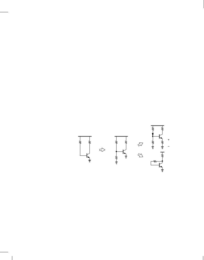
The bias topology of Fig. 5.19 is used extensively in discrete circuits and occasionally in integrated circuits. Illustrated in Fig. 5.21, two rules are typically followed: (1) I1 IB to lower sensitivity to , and (2) VRE must be large enough (100 mV to several hundred millivolts) to suppress the effect of uncertainties in VX and VBE.
BR |
Wiley/Razavi/Fundamentals of Microelectronics [Razavi.cls v. 2006] |
June 30, 2007 at 13:42 |
192 (1) |
|
|
|
|
192 |
|
|
|
|
|
|
|
|
|
|
|
|
|
|
|
|
|
|
|
Chap. 5 |
Bipolar Amplifiers |
||
|
|
|
|
|
|
|
|
|
|
|
|
|
|
|
VCC |
|
|
|
|
||||
|
|
|
|
|
|
|
|
|
|
|
|
|
|
|
|
|
|
|
|||||
R 1 |
|
|
|
|
|
|
|
|
|
|
|
RC |
Small Enough to |
|
|
|
|||||||
I 1 |
|
|
|
|
|
|
Y |
|
|
I C |
Avoid Saturation |
|
|
|
|||||||||
|
|
|
|
|
|
|
|
|
|
|
|
|
|||||||||||
|
|
|
|
|
|
|
|
|
|
|
|
|
|||||||||||
|
|
|
|
|
|
|
|
|
|
|
|
|
|
|
|
||||||||
I 1 >>I B |
|
|
|
X |
|
|
|
|
Q 1 |
|
|
|
|
|
|||||||||
|
|
|
|
|
|
||||||||||||||||||
R 2 |
|
|
|
I B |
|
|
|
|
|
|
|
|
|
||||||||||
|
|
|
|
|
|
|
|
|
|
|
|
|
|
|
|
|
|
|
|||||
|
|
|
|
|
|
|
|
|
|
|
|
|
|
|
|
|
|||||||
|
|
|
|
|
|
|
R E |
|
|
|
V |
|
>> Variations in V |
|
and V |
||||||||
|
|
|
|
|
|
|
|
|
|||||||||||||||
|
|
|
|
|
|
|
|
|
|
|
|
|
|
|
RE |
|
X |
|
BE |
||||
|
|
|
|
|
|
|
|
|
|
|
|
|
|
|
|
|
|
|
|
|
|
|
|
Figure 5.21 Summary of robust bias conditions.
Design Procedure It is possible to prescribe a design procedure for the bias topology of Fig. 5.21 that serves most applications: (1) decide on a collector bias current that yields proper small-signal parameters such as gm and r ; (2) based on the expected variations of R1, R2, and VBE, choose a value for VRE ICRE, e.g., 200 mV; (3) calculate VX = VBE + IC RE with VBE = VT ln(IC=IS); (4) choose R1 and R2 so as to provide the necessary value of VX and establish I1 IB. Determined by small-signal gain requirements, the value of RC is bounded by a maximum that places Q1 at the edge of saturation. The following example illustrates these concepts.
Example 5.11
Design the circuit of Fig. 5.21 so as to provide a transconductance of 1=(52 ) for Q1. Assume VCC = 2:5 V, = 100, and IS = 5 10,17 A. What is the maximum tolerable value of RC?
Solution
A gm of (52 ),1 translates to a collector current of 0.5 mA and a VBE of 778 mV. Assuming REIC = 200 mV, we obtain RE = 400 . To establish VX = VBE + REIC = 978 mV, we must have
|
R2 |
|
|
|
(5.63) |
||
|
|
|
VCC |
= VBE + REIC; |
|||
|
R1 + R2 |
||||||
where the base current is neglected. For the base current IB = 5 A to be negligible, |
|
||||||
|
|
|
VCC |
|
I ; |
(5.64) |
|
|
|
|
|
|
|
||
|
|
|
|
|
|
B |
|
|
|
R1 + R2 |
|
||||
e.g., by a factor of 10. Thus, R1 + R2 = 50 k , which in conjunction with (5.63) yields |
|
||||||
|
|
R1 |
= 30:45 k |
(5.65) |
|||
|
|
R2 |
= 19:55 k : |
(5.66) |
|||
How large can RC be? Since the collector voltage is equal to VCC , RCIC, we pose the following constraint to ensure active mode operation:
VCC , RCIC > VX ; |
(5.67) |
that is, |
|
RCIC < 1:522 V: |
(5.68) |

BR |
Wiley/Razavi/Fundamentals of Microelectronics [Razavi.cls v. 2006] |
June 30, 2007 at 13:42 |
193 (1) |
|
|
|
|
Sec. 5.2 |
Operating Point Analysis and Design |
193 |
Consequently, |
|
|
|
RC < 3:044 k : |
(5.69) |
If RC exceeds this value, the collector voltage falls below the base voltage. As mentioned in Chapter 4, the transistor can tolerate soft saturation, i.e., up to about 400 mV of base-collector forward bias. Thus, in low-voltage applications, we may allow VY VX , 400 mV and hence a greater value for RC.
Exercise
Repeat the above example if the power budget is only 1 mW and the transconductance of Q1 is not given.
The two rules depicted in Fig. 5.21 to lower sensitivities do impose some trade-offs. Specifically, an overly conservative design faces the following issues: (1) if we wish I1 to be much much greater than IB, then R1 + R2 and hence R1 and R2 are quite small, leading to a low input impedance; (2) if we choose a very large VRE, then VX (= VBE + VRE) must be high, thereby limiting the minimum value of the collector voltage to avoid saturation. Let us return to the above example and study these issues.
Example 5.12
Repeat Example 5.11 but assuming VRE = 500 mV and I1 100IB.
Solution
The collector current and base-emitter voltage remain unchanged. The value of RE is now given by 500 mV=0:5 mA = 1 k . Also, VX = VBE + REIC = 1:278 V and (5.63) still holds. We rewrite (5.64) as
|
VCC |
100IB; |
(5.70) |
|
|
|
|
||
|
R1 + R2 |
|
||
obtaining R1 + R2 = 5 k . It follows that |
|
|
|
|
|
R1 |
= 1:45 k |
(5.71) |
|
|
R2 |
= 3:55 k : |
(5.72) |
|
Since the base voltage has risen to 1.278 V, the collector voltage must exceed this value to avoid saturation, leading to
RC < |
VCC , VX |
(5.73) |
|
IC |
|
< |
1:044 k : |
(5.74) |
As seen in Section 5.3.1, the reduction in RC translates to a lower voltage gain. Also, the much smaller values of R1 and R2 here than in Example 5.11 introduce a low input impedance, loading the preceding stage. We compute the exact input impedance of this circuit in Section 5.3.1.
BR |
Wiley/Razavi/Fundamentals of Microelectronics [Razavi.cls v. 2006] |
June 30, 2007 at 13:42 |
194 (1) |
|
|
|
|
194 |
Chap. 5 |
Bipolar Amplifiers |
Exercise
Repeat the above example if VRE is limited to 100 mV.
5.2.4 Self-Biased Stage
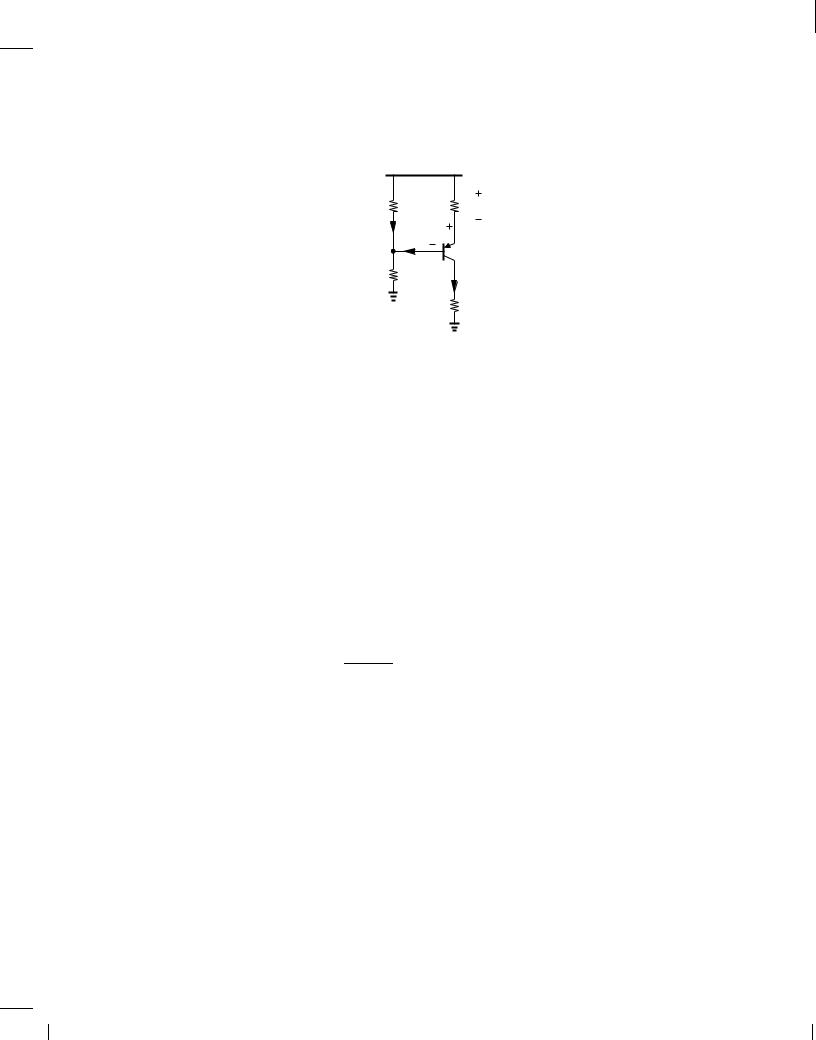
Another biasing scheme commonly used in discrete and integrated circuits is shown in Fig. 5.22. Called “self-biased” because the base current and voltage are provided from the collector, this stage exhibits many interesting and useful attributes.
RB
I B
X
VCC
RC  Y
Y  I C
I C

 Q 1
Q 1
Figure 5.22 Self-biased stage.
Let us begin the analysis of the circuit with the observation that the base voltage is always lower than the collector voltage: VX = VY , IBRB. A result of self-biasing, this important property guarantees that Q1 operates in the active mode regardless of device and circuit parameters. For example, if RC increases indefinitely, Q1 remains in the active region, a critical advantage over the circuit of Fig. 5.21.
We now determine the collector bias current by assuming IB IC ; i.e., RC carries a current equal to IC, thereby yielding
VY = VCC , RCIC: |
(5.75) |
||
Also, |
|
||
VY = RBIB + VBE |
(5.76) |
||
= RBIC + VBE: |
(5.77) |
||
|
|
||
Equating the right hand sides of (5.75) and (5.77) gives |
|
||
IC = VCC , VBE : |
(5.78) |
||
RC + |
RB |
|
|
|
|
||
|
|
||
As usual, we begin with an initial guess for VBE, compute IC, and utilize VBE = VT ln(IC =IS) to improve the accuracy of our calculations.
Example 5.13
Determine the collector current and voltage of Q1 in Fig. 5.22 if RC = 1 k , RB = 10 k , VCC = 2:5 V, IS = 5 10,17 A, and = 100. Repeat the calculations for RC = 2 k .

BR |
Wiley/Razavi/Fundamentals of Microelectronics [Razavi.cls v. 2006] |
June 30, 2007 at 13:42 |
195 (1) |
|
|
|
|
Sec. 5.2 |
Operating Point Analysis and Design |
195 |
Solution
Assuming VBE = 0:8 V, we have from (5.78):
IC = 1:545 mA; |
(5.79) |
and hence VBE = VT ln(IC =IS) = 807:6 mV, concluding that the initial guess for VBE and the value of IC given by it are reasonably accurate. We also note that RB IB = 154:5 mV and
VY = RBIB + VBE 0:955 V.
If RC = 2 k , then with VBE = 0:8 V, Eq. (5.78) gives
IC = 0:810 mA: |
(5.80) |
To check the validity of the initial guess, we write VBE = VT ln(IC =IS) = 791 mV. Compared with VCC , VBE in the numerator of (5.78), the 9-mV error is negligible and the value of IC in (5.80) is acceptable. Since RBIB = 81 mV, VY 0:881 V.
Exercise
What happens if the base resistance is doubled?
Equation (5.78) and the above example suggest two important guidelines for the design of the self-biased stage: (1) VCC , VBE must be much greater than the uncertainties in the value of VBE; (2) RC must be much greater than RB= to lower sensitivity to . In fact, if RC RB= , then
IC |
VCC , VBE ; |
(5.81) |
|
RC |
|
and VY = VCC , ICRC VBE. This result serves as a quick estimate of the transistor bias conditions.
Design Procedure Equation (5.78) together with the condition RC RB= provides the basic expressions for the design of the circuit. With the required value of IC known from smallsignal considerations, we choose RC = 10RB= and rewrite (5.78) as
IC |
= VCC , VBE ; |
(5.82) |
||
|
|
1:1RC |
|
|
where VBE = VT ln(IC=IS). That is, |
|
|
|
|
R |
= VCC , VBE |
(5.83) |
||
C |
|
1:1IC |
|
|
|
|
|
||
RB |
= |
RC |
: |
(5.84) |
10 |
||||
The choice of RB also depends on small-signal requirements and may deviate from this value, but it must remain substantially lower than RC.
Example 5.14
Design the self-biased stage of Fig. 5.22 for gm = 1=(13 ) and VCC = 1:8 V. Assume
IS = 5 10,16 A and = 100.
BR |
Wiley/Razavi/Fundamentals of Microelectronics [Razavi.cls v. 2006] |
June 30, 2007 at 13:42 |
196 (1) |
|
|
|
|
196 Chap. 5 Bipolar Amplifiers
Solution
Since gm = IC=VT = 1=(13 ), we have IC = 2 mA, VBE = 754 mV, and |
|
|
R VCC , VBE |
(5.85) |
|
C |
1:1IC |
|
|
|
|
475 : |
(5.86) |
|
Also, |
|
|
RB |
= RC |
(5.87) |
|
10 |
|
|
= 4:75 k : |
(5.88) |
Note that RBIB = 95 mV, yielding a collector voltage of 754 mV + 95 mV = 849 mV.
Exercise
Repeat the above design with a supply voltage of 2.5 V.
Figure 5.23 summarizes the biasing principles studied in this section.
|
|
|
|
R 1 |
|
RC |
|
|
|
|
I 1 |
|
Q 1 |
|
|
|
|
|
|
|
R B |
RC |
R 1 |
RC |
R 2 |
R E |
VRE |
Q 1 |
Q 1 |
RC |
|
R 2 |
|||
|
RB |
||
|
|
Always in |
|
Sensitive |
Sensitive |
Q 1 Active Mode |
|
to β |
to Resistor Errors |
|
Figure 5.23 Summary of biasing techniques.
5.2.5 Biasing of PNP Transistors
The dc bias topologies studied thus far incorporate npn transistors. Circuits using pnp devices follow the same analysis and design procedures while requiring attention to voltage and current polarities. We illustrate these points with the aid of some examples.
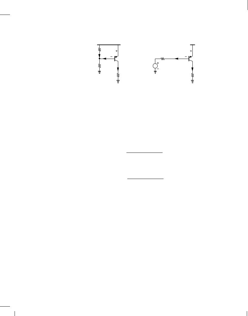
Example 5.15
Calculate the collector and voltage of Q1 in the circuit of Fig. 5.24 and determine the maximum allowable value of RC for operation in the active mode.
Solution
The topology is the same as that in Fig. 5.13 and we have,
IBRB + VEB = VCC : |
(5.89) |

BR |
Wiley/Razavi/Fundamentals of Microelectronics [Razavi.cls v. 2006] |
June 30, 2007 at 13:42 |
197 (1) |
|
|
|
|
Sec. 5.2 |
Operating Point Analysis and Design |
197 |
|
I B |
VCC |
|
VEB |
|
|
|
Q 1 |
|
|
X |
|
R B |
Y |
|
I C |
|
|
|
|
|
|
RC |
Figure 5.24 Simple biasing of pnp stage.
That is, |
|
|
|
IB = |
VCC |
, VEB |
(5.90) |
|
RB |
|
|
and |
|
|
|
I = VCC |
, VEB : |
(5.91) |
|
C |
|
RB |
|
|
|
|
|
The circuit suffers from sensitivity to .
If RC is increased, VY rises, thus approaching VX (= VCC ,VEB) and bringing Q1 closer to saturation. The transistor enters saturation at VY = VX , i.e.,
IC RC;max = VCC , VEB |
(5.92) |
|||
and hence |
|
|
|
|
R |
= |
VCC , VEB |
(5.93) |
|
C;max |
|
|
IC |
|
|
|
|
|
|
|
= |
RB |
: |
(5.94) |
|
|
|||
|
|
|
|
|
From another perspective, since VX = IB RB and VY = IC RC, we have IBRB = IC RC;max as the condition for edge of saturation, obtaining RB = RC;max.
Exercise
For a given RC, what value of RB places the device at the edge of saturation?
Example 5.16
Determine the collector current and voltage of Q1 in the circuit of Fig. 5.25(a).
Solution
As a general case, we assume IB is significant and construct the Thevenin equivalent of the voltage divider as depicted in Fig. 5.25(b):
|
R1 |
(5.95) |
|
VT hev = |
|
VCC |
|
R1 + R2 |
|||
RT hev = R1jjR2: |
(5.96) |
||
BR |
Wiley/Razavi/Fundamentals of Microelectronics [Razavi.cls v. 2006] |
June 30, 2007 at 13:42 |
198 (1) |
|
|
|
|
198 |
|
|
Chap. 5 |
Bipolar Amplifiers |
|
|
VCC |
|
VCC |
R 2 |
VEB |
|
RThev I B |
VEB |
I 1 |
|
|||
I B |
Q 1 |
Q 1 |
||
|
X |
|
||
|
|
|
X |
|
R 1 |
Y |
VThev |
|
Y |
|
|
I C |
|
I C |
|
|
RC |
|
RC |
|
(a) |
|
(b) |
|
Figure 5.25 (a) PNP stage with resistive divider biasing, (b) Thevenin equivalent of divider and VCC.
Adding the voltage drop across RT hev and VEB to VT hev yields
VT hev + IB RT hev + VEB = VCC; |
(5.97) |
||||||
that is, |
|
|
|
|
|
|
|
IB = VCC , VT hev , VEB |
(5.98) |
||||||
|
|
RT hev |
|
|
|||
|
|
R2 |
|
VCC |
, VEB |
|
|
|
R + R |
|
(5.99) |
||||
= |
1 |
2 |
|
|
: |
||
|
|
RT hev |
|
|
|||
It follows that |
|
|
|
|
|
|
|
|
|
R2 |
|
|
VCC |
, VEB |
|
|
|
R + R |
(5.100) |
||||
I = |
1 |
2 |
|
: |
|||
C |
|
|
RT hev |
|
|
||
|
|
|
|
|
|||
As in Example 5.9, some iteration between IC and VEB may be necessary.
Equation (5.100) indicates that if IB is significant, then the transistor bias heavily depends on . On the other hand, if IB I1, we equate the voltage drop across R2 to VEB, thereby obtaining the collector current:
|
R2 |
|
VCC = VEB |
(5.101) |
||
|
R1 + R2 |
|||||
IC = IS exp |
|
R2 |
VCC : |
(5.102) |
||
|
|
|
||||
|
|
R1 |
+ R2 |
VT |
|
|
Note that this result is identical to Eq. (5.30).
Exercise
What is the maximum value of RC is Q1 must remain in soft saturation?
Example 5.17
Assuming a negligible base current, calculate the collector current and voltage of Q1 in the
BR |
Wiley/Razavi/Fundamentals of Microelectronics [Razavi.cls v. 2006] |
June 30, 2007 at 13:42 |
199 (1) |
|
|
|
|
Sec. 5.2 Operating Point Analysis and Design 199
circuit of Fig. 5.26. What is the maximum allowable value of RC for Q1 to operate in the forward active region?
|
VCC |
|
R 2 |
R E VRE |
|
I 1 |
VEB |
|
I B |
||
|
Q 1 |
|
|
X |
|
R 1 |
Y |
|
I C |
||
|
||
|
RC |
Figure 5.26 PNP stage with degeneration resistor.
Solution
With IB I1, we have VX = VCCR1=(R1 + R2). Adding to VX the emitter-base voltage and the drop across RE, we obtain
VX + VEB + REIE = VCC |
(5.103) |
||||
and hence |
|
|
|
|
|
IE = |
1 |
|
R2 |
VCC , VEB : |
(5.104) |
|
|
||||
|
RE |
R1 + R2 |
|
||
Using IC IE, we can compute a new value for VEB and iterate if necessary. Also, with IB = IC = , we can verify the assumption IB I1.
In arriving at (5.104), we have written a KVL from VCC to ground, Eq. (5.103). But a more straightforward approach is to recognize that the voltage drop across R2 is equal to VEB +IERE, i.e.,
R2 |
|
(5.105) |
VCC R1 + R2 |
= VEB + IERE; |
which yields the same result as in (5.104).
The maximum allowable value of RC is obtained by equating the base and collector voltages:
VCC |
|
R1 |
= RC;maxIC |
|
|
|
|
|
|
(5.106) |
|||
R1 |
+ R2 |
|
|
|
|
|
|
||||||
|
|
|
|
RC;max |
|
|
R2 |
VCC , VEB : |
(5.107) |
||||
|
|
|
R1 + R2 |
||||||||||
|
|
|
|
|
RE |
|
|
|
|
||||
It follows that |
|
|
|
|
|
|
|
|
|
|
|
|
|
RC;max = REVCC |
R1 |
|
|
|
1 |
: |
(5.108) |
||||||
R1 + R2 |
|
|
R2 |
|
VCC , VEB |
||||||||
|
|
|
|
|
|
|
|
|
R1 + R2 |
|
|
||
BR |
Wiley/Razavi/Fundamentals of Microelectronics [Razavi.cls v. 2006] |
June 30, 2007 at 13:42 |
200 (1) |
|
|
|
|
200 |
Chap. 5 |
Bipolar Amplifiers |
Exercise
Repeat the above example if R2 = 1.
Example 5.18
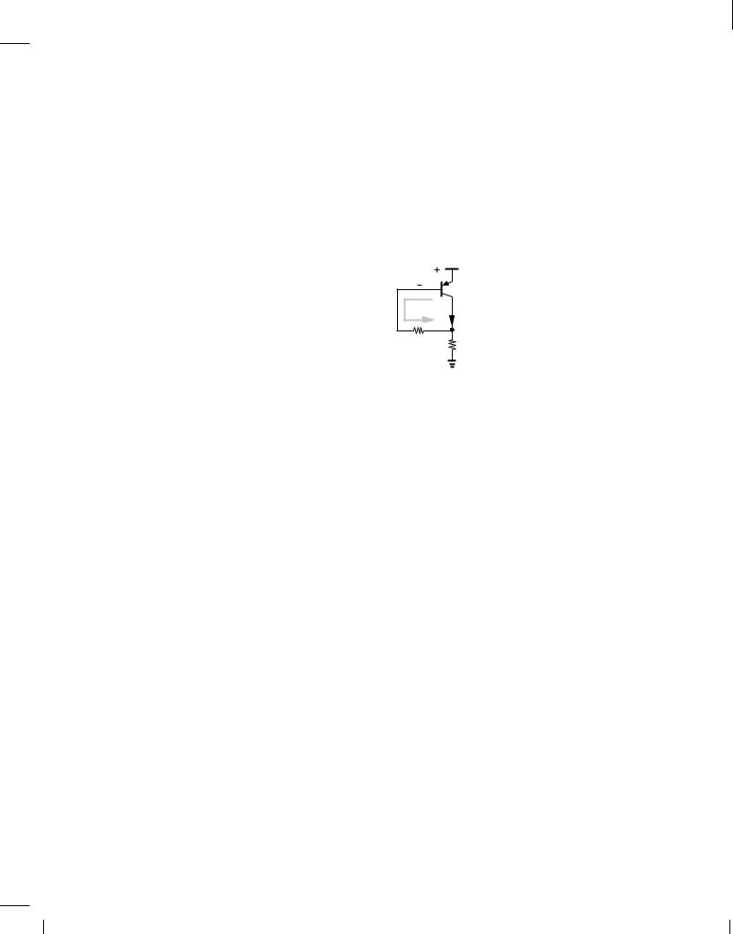
Determine the collector current and voltage of Q1 in the self-biased circuit of Fig. 5.27.
VEB |
VCC |
|
X |
Q 1 |
|
|
|
|
I B |
Y |
|
|
I C |
|
R B |
R |
C |
|
|
|
Figure 5.27 Self-biased pnp stage.
Solution
We must write a KVL from VCC through the emitter-base junction of Q1, RB, and RC to ground. Since 1 and hence IC IB, RC carries a current approximately equal to IC, creating VY = RCIC. Moreover, VX = RBIB + VY = RBIB + RCIC, yielding
VCC = VEB |
+ VX |
|
|
|
|
(5.109) |
||
= VEB |
+ RBIB + IC RC |
|
|
(5.110) |
||||
= V |
+ |
RB |
+ R |
C |
I |
C |
: |
(5.111) |
|
||||||||
EB |
|
|
|
|
|
|||
|
|
|
|
|
|
|
||
Thus,
IC = |
VCC , VEB ; |
(5.112) |
||
|
|
RB |
+ RC |
|
|
|
|
|
|
|
|
|
|
|
a result similar to Eq. (5.78). As usual, we begin with a guess for VEB, compute IC , and determine a new value for VEB, etc. Note that, since the base is higher than the collector voltage, Q1 always remains in the active mode.
Exercise
How far is Q1 from saturation?