

ADS8339
www.ti.com |
SBAS677A –JUNE 2014 –REVISED OCTOBER 2014 |
9.3 Feature Description
9.3.1 Analog Input
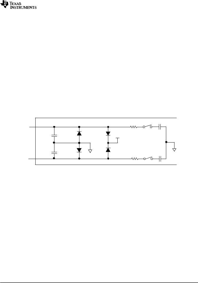
When the converter samples the input, the voltage difference between the +IN and –IN inputs is captured on the internal capacitor array. The differential signal range is [(+IN) – (–IN)]. The voltage on +IN is limited between
GND – 0.1 V and Vref + 0.1 V and the voltage on –IN is limited between GND – 0.1 V to GND + 0.1 V. The input rejects any small signal that is common to both the +IN and –IN input.
The (peak) input current through the analog input depends upon a number of factors: sample rate, input voltage, and source impedance. The current into the device charges the internal capacitor array (as shown in Figure 45) during the sample period. When this capacitance is fully charged, there is no further input current. The source of the analog input voltage must be able to charge the input capacitance (59 pF) to a 18-bit settling level within the minimum acquisition time. When the converter goes into hold mode, the input impedance is greater than 1 GΩ.
Care must be taken regarding the absolute analog input voltage. To maintain linearity of the converter, the +IN input, –IN input, and span [+IN – (–IN)] must be within the limits specified. Outside of these ranges, the converter linearity may not meet specifications.
Care must also be taken to ensure that the output impedance of the sources driving the +IN input and the –IN input is matched. If this output impedance is not well matched, the two inputs can have different settling times. This mismatch may result in an offset error, gain error, and linearity error that changes with temperature and input voltage. Typically, the –IN input is grounded at the input decoupling capacitor.
Device in Hold Mode |
55 pF |
|
218 W |
+IN |
|
4 pF |
|
+VA |
|
AGND |
|
4 pF |
|
|
55 pF |
|
218 W |
-IN |
|
Figure 45. Input Equivalent Circuit
9.3.2 Power Saving
The device has an auto power-down feature. The device powers down at the end of every conversion. The input signal is acquired on sampling capacitors when the device is in power-down state. At the same time, the conversion results are available for reading. The device powers up automatically at the start of the conversion. The conversion runs on an internal clock and requires a fixed time. As a result, device power consumption is directly proportional to the speed of operation.
Copyright © 2014, Texas Instruments Incorporated |
Submit Documentation Feedback |
17 |
Product Folder Links: ADS8339