

ADS8339
SBAS677A –JUNE 2014–REVISED OCTOBER 2014 |
www.ti.com |
9 Detailed Description
9.1 Overview
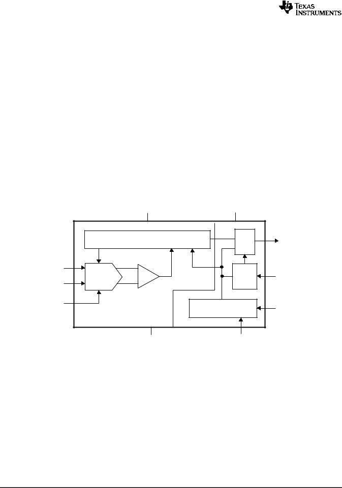
The ADS8339 is a 250-kSPS, low-power, successive-approximation register (SAR), analog-to-digital converter (ADC) that uses an external reference. The architecture is based on charge redistribution, which inherently includes a sample-and-hold function.
The ADS8339 is a single-channel device. The analog input is provided to two input pins: +IN and –IN, where –IN is a pseudo-differential input and has a limited range of ±0.1 V. When a conversion is initiated, the differential input on these pins is sampled on the internal capacitor array. While a conversion is in progress, both the +IN and –IN inputs are disconnected from any internal functions.
The device has an internal clock that is used to run the conversion. Therefore, the conversion requires a fixed amount of time. After a conversion is completed, the device reconnects the sampling capacitors to the +IN and –IN pins and the device is in the acquisition phase. During this phase, the device is powered down and conversion data can be read.
The device digital output is available in SPI-compatible format. The device easily interfaces with microprocessors, digital signal processors (DSPs), or field-programmable gate arrays (FPGAs).
9.2 Functional Block Diagram
+VA |
+VBD |
|
SAR |
Output |
SDO |
|
Drive |
|
|
|
|
Comparator |
|
|
IN+ |
Input |
|
|
|
|
CDAC |
Shift |
SDI |
IN- |
Register |
|
REFIN |
Conversion and I/O |
SCLK |
|
||
|
Control Logic |
|
|
|
|
DEVICE |
|
|
GND |
CONVST |
|
16 |
Submit Documentation Feedback |
Copyright © 2014, Texas Instruments Incorporated |
Product Folder Links: ADS8339