

ADS8339
www.ti.com |
SBAS677A –JUNE 2014 –REVISED OCTOBER 2014 |
Application Information (continued)
10.1.1.1 Reference Driver Circuit
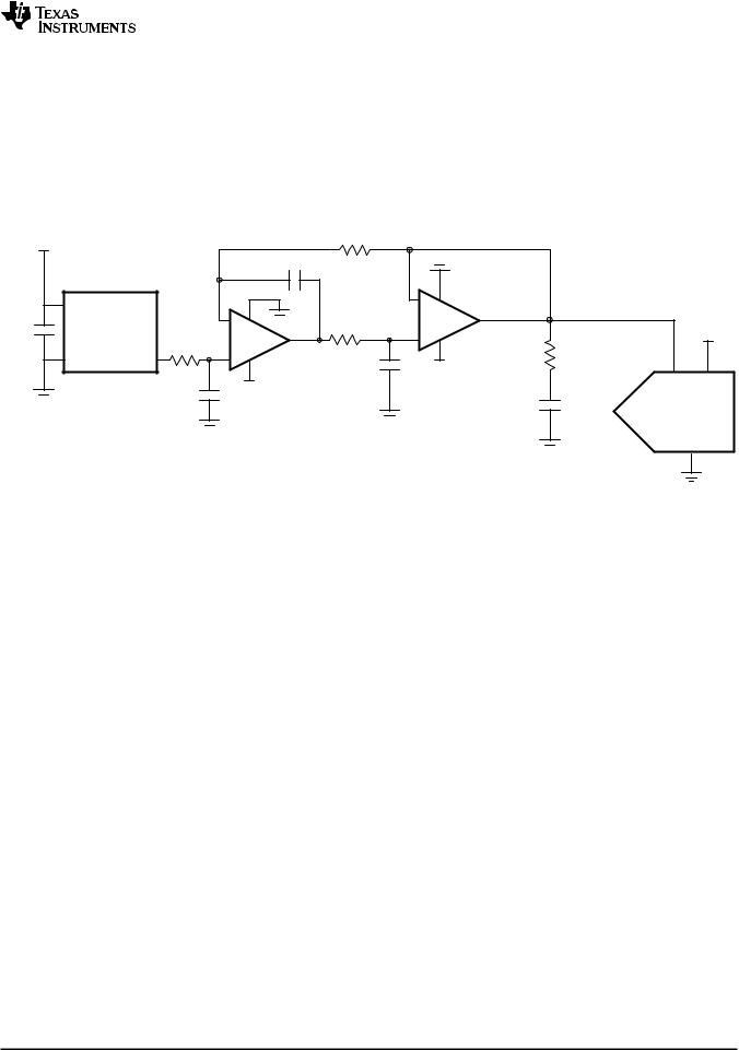
A more detailed circuit shows the schematic (as shown in Figure 59) of a complete reference driver circuit that generates 4.5 V dc using a single 5-V supply. This circuit can drive the reference pin of the ADS8339 at sampling rates of up to 250 kSPS. The 4.5-V reference voltage is generated using a high-precision, low-noise REF5045. The output broadband noise of the reference is further filtered using a low-pass filter with a 3-dB cutoff frequency of 16 Hz.
20 k
AVDD |
|
|
|
|
|
|
|
|
|
|
|
|
|
1 µF |
|
|
|
REF5045 |
|
|
|
|
|
|
|
|
VIN |
|
|
|
|
|
- |
|
|
|
|
|
|
|
|
|
|
|
1 µF |
|
|
- |
|
|
1 k |
|
|
|
|
|
|
|
+ + |
|
AVDD |
|
|
|
10 k |
|
+ |
|
THS4281 |
||
GND |
OUT |
|
+ |
OPA333 |
1 µF |
0.2 |
|
|
|
|
|
AVDD |
|
AVDD |
|
REFIN +VA |
|
|
|
1 µF |
|
|
10 µF |
IN+ |
||
|
|
|
|
|
|
V+ |
||
|
|
|
|
|
|
|
Device |
|
|
|
|
|
|
|
|
|
|
|
|
|
|
|
|
|
|
-IN |
|
|
|
|
|
|
|
|
GND |
Figure 59. Reference Driver Circuit Schematic
The driver also includes a THS4281 and an OPA333. This composite architecture provides superior ac and dc performance at reduced power levels compared to a single high-performance amplifier.
The THS4281 is a high-bandwidth amplifier with very low output impedance of 1 Ω at a frequency of 1 MHz. The low output impedance makes the THS4281 a good choice for driving large capacitive loads. The high offset and drift specifications of the THS4281 are corrected using a dc-correcting amplifier (OPA333) inside the feedback loop. Thus, the composite scheme also inherits the extremely low offset and temperature drift specifications of the OPA333.
10.1.2 ADC Input Driver
The input driver circuit for a high-precision ADC mainly consists of two parts: a driving amplifier and an RC filter. An amplifier is used for signal conditioning the input voltage. The low output impedance of the amplifier functions as a buffer between the signal source and the sampling capacitor input of the ADC. The RC filter functions as an antialiasing filter that band-limits the wideband noise contributed by the front-end circuit. The RC filter also helps attenuate the sampling capacitor charge injection from the switched-capacitor input stage of the ADC. Careful design of the front-end circuit is critical to meet the linearity and noise performance of a high-precision, 16-bit ADC such as the ADS8339.
Copyright © 2014, Texas Instruments Incorporated |
Submit Documentation Feedback |
27 |
Product Folder Links: ADS8339

ADS8339
SBAS677A –JUNE 2014–REVISED OCTOBER 2014 |
www.ti.com |
Application Information (continued)
10.1.2.1 Input Amplifier Selection
Selection criteria for the input amplifier is dependent on the input signal type as well as performance goals of the data acquisition system. Some key specifications to consider when selecting an amplifier to drive the inputs of the ADS8339 are:
•Small-signal bandwidth. The small-signal bandwidth of the input amplifier must be as high as possible for a given power budget. Higher bandwidth reduces the closed-loop output impedance of the amplifier, thus allowing the amplifier to more easily drive the RC filter (with low cutoff frequency) at the inputs of the ADC. Higher bandwidth also minimizes harmonic distortion at higher input frequencies. In order to maintain overall stability, the amplifier bandwidth must satisfy Equation 1:
§ |
|
1 |
· |
|
¨ |
|
|
¸ |
|
|
|
|
||
Unity Gain Bandwidth t 4 u¨ |
|
|
¸ |
|
© |
2S u (RFLT |
RFLT ) uCFLT ¹ |
(1) |
|
•Noise. Noise contribution of the front-end amplifiers must be as low as possible to prevent any degradation in the overall SNR performance of the system. As a rule of thumb, to ensure that the noise performance of the data acquisition system is not limited by the front-end circuit, keep the total noise contribution from the frontend circuit below 20% of the input-referred noise of the ADC. Noise from the input driver circuit gets bandlimited by the RC filter, as given in Equation 2.
|
|
|
|
§ V1 |
|
|
· |
2 |
|
|
|
|
|
|
§ |
SNR dB · |
||||||
|
|
|
|
|
|
|
|
S |
|
|
|
1 |
|
VREF |
¨ |
|
¸ |
|||||
|
|
|
|
|
|
|
|
|
|
|
|
|
||||||||||
N |
u |
2 u |
¨ |
|
f |
_ AMP_ PP ¸ |
e2 |
u |
u f |
|
d |
u |
u10 © |
20 ¹ |
||||||||
¨ |
|
|
|
¸ |
|
3dB |
|
|
|
|
||||||||||||
|
|
|
|
|
|
|
|
|
|
|||||||||||||
G |
|
|
|
|
|
6.6 |
n _ RMS |
2 |
|
5 |
2 |
|
|
|
|
|||||||
|
|
|
|
¨ |
|
|
¸ |
|
|
|
|
|
|
|
||||||||
|
|
|
|
© |
|
|
|
¹ |
|
|
|
|
|
|
|
|
|
|
|
|
|
|
where:
• V1 / f_AMP_PP is the peak-to-peak flicker noise in µV, |
|
|||
• en_RMS is the amplifier broadband noise density in nV/√ |
Hz, |
|
|
|
• |
f–3dB is the 3-dB bandwidth of the RC filter, and |
|
||
• |
NG is the noise gain of the front-end circuit, which is equal to 1 in a buffer configuration. |
(2) |
||
•Distortion. The ADC and the input driver introduce nonlinearity in a data acquisition block. As a rule of thumb, to ensure that the distortion performance of the data acquisition system is not limited by the front-end circuit, the distortion of the input driver must be at least 10 dB lower than the distortion of the ADC, as given in Equation 3.
THDAMP d THDADC 10 dB |
(3) |
•Settling Time. For dc signals with fast transients that are common in a multiplexed application, the input signal must settle to a 16-bit accuracy level at the device inputs during the acquisition time. This condition is critical in maintaining the overall linearity of the ADC. Typically, the amplifier data sheets specify the output settling performance only up to 0.1% to 0.001%, which may not be sufficient for the desired 16-bit accuracy. Therefore, the settling behavior of the input driver must always be verified by TINA™-SPICE simulations before selecting the amplifier.
10.1.2.2 Antialiasing Filter
Converting analog-to-digital signals requires sampling the input signal at a constant rate. Any frequency content in the input signal that is beyond half the sampling frequency is folded back into the low-frequency spectrum, which is undesirable. This process is called aliasing. An analog antialiasing filter must be used to remove the high-frequency component (beyond half the sampling frequency) from the input signal before being sampled by the ADC.
An antialiasing filter is designed as a low-pass, RC filter for which the 3-dB bandwidth is optimized based on specific application requirements. For dc signals with fast transients (including multiplexed input signals), a highbandwidth filter is designed to allow for accurate settling of the signal at the input of the ADC. For ac signals, keep the filter bandwidth as low as possible to band-limit the noise fed into the ADC, which improves the signal- to-noise ratio (SNR) performance of the system.
28 |
Submit Documentation Feedback |
Copyright © 2014, Texas Instruments Incorporated |
Product Folder Links: ADS8339
ADS8339
www.ti.com |
SBAS677A –JUNE 2014 –REVISED OCTOBER 2014 |
Application Information (continued)
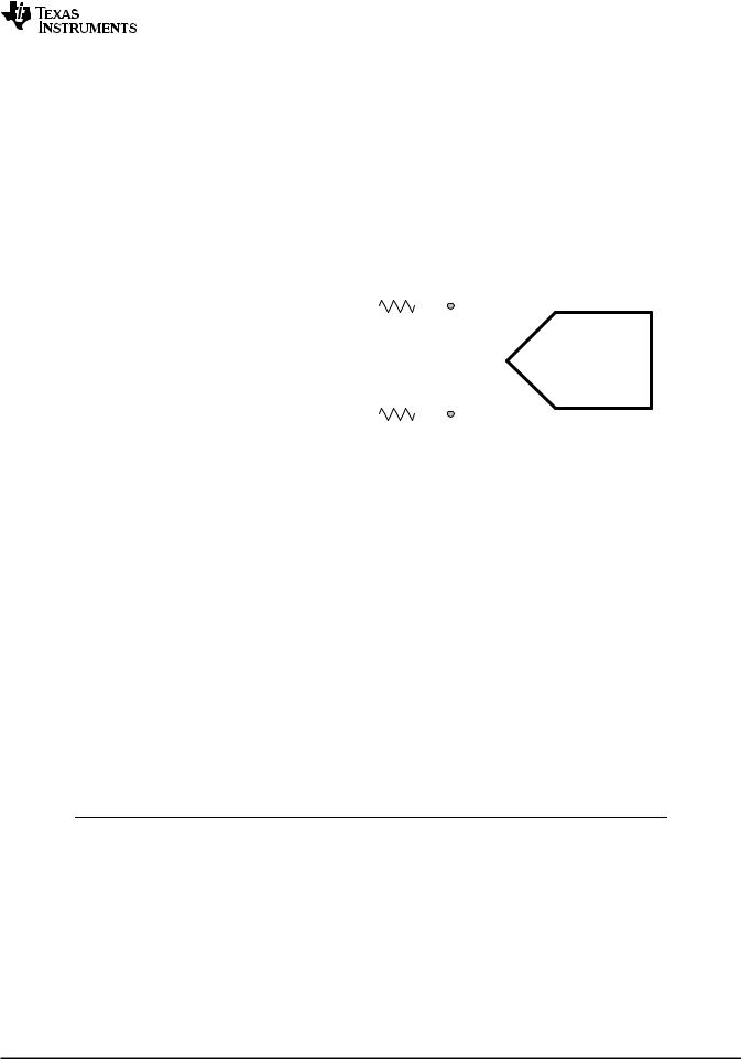
The RC filter also helps absorb the sampling charge injection from the switched-capacitor input of the ADC. A filter capacitor, CFLT, is connected across the inputs of the ADC (as shown in Figure 60). This capacitor helps absorb the sampling capacitor charge injection in addition to functioning as a charge bucket to quickly charge the internal sample-and-hold capacitors during the acquisition phase.
When selecting this capacitor, as a rule of thumb, the capacitor value must be at least 10 times the ADC sampling capacitor specified on the data sheet. The input sampling capacitance is approximately 59 pF for the ADS8339. The value of CFLT must be greater than 590 pF. The capacitor must be a COGor NPO-type because these capacitor types have a high-Q, low-temperature coefficient and stable electrical characteristics under varying voltages, frequency, and time.
|
|
|
|
|
|
|
|
|
|
|
RFLT ”44 |
|
|
|
|
|
|
|
|
|
|
|
||||
f |
|
1 |
|
|
|
|
|
|
|
|
|
|
|
|
|
|
|
VIN+ |
|
|
|
|
|
|
|
|
|
|
|
|
|
|
|
|
|
|
|
|
|
|
|
|
|
|
|
|
|
|
|
|
|||
|
|
|
|
|
|
|
|
|
|
|
|
|
|
|
|
|
|
|
|
|
|
|
||||
|
|
|
|
|
|
|
|
|
|
|
|
|
|
+ |
|
|
|
|
|
|
|
|
||||
3dB |
|
|
|
CFLT •590 pF |
|
|
|
|
|
|
|
|
|
|
|
|||||||||||
2S u RFLT RFLT |
u CFLT |
|
|
|
Device |
|||||||||||||||||||||
|
|
|
||||||||||||||||||||||||
|
|
|
|
|
|
|
-IN |
|||||||||||||||||||
|
|
|
|
|
|
|
||||||||||||||||||||
|
|
|
|
|
|
|
|
|
|
|
|
|
|
|
|
|
|
GND |
||||||||
|
|
|
|
|
|
|
|
|
|
|
|
|
|
|
|
|
|
|||||||||
|
|
|
|
|
|
|
|
|
|
|
|
|
|
|
|
|
|
|
||||||||
|
|
|
|
|
|
|
|
|
|
|
|
|
|
|
|
|
|
|
|
|
|
|
|
|
|
|
|
|
|
|
|
|
|
|
|
|
|
RFLT ”44 |
|
|
|
|
|
|
|
|
|
|
|
||||
|
|
|
|
|
|
|
|
|
|
|
|
|
|
|
|
|
|
|
|
|
|
|||||
|
|
|
|
|
|
|
|
|
|
|
|
|
|
|
|
|||||||||||
|
|
|
|
|
|
|
|
|
|
|
|
|
|
|
|
|
|
|
|
|
|
|
|
|
|
|
|
|
|
|
|
|
|
|
|
|
|
|
|
|
|
|
|
|
|||||||||
|
|
|
Figure 60. |
Antialiasing Filter |
|
|
|
|
|
|
|
|
|
|
|
|||||||||||
|
|
|
|
|
|
|
|
|
|
|
|
|
|
|
|
|
|
|
|
|
|
|
|
|
|
|
NOTE
Driving capacitive loads can degrade the phase margin of the input amplifiers, thus making the amplifier marginally unstable. To avoid stability issues, series isolation resistors (RFLT) are used at the output of the amplifiers. A higher value of RFLT is helpful from the amplifier stability perspective. Distortion increases with source impedance, input signal frequency, and input signal amplitude. The selection of RFLT thus requires a balance between stability and distortion of the design.
TI recommends limiting the value of RFLT to a maximum of 44 Ω in order to avoid any significant degradation in linearity performance for the ADS8339. The tolerance of resistors can be 1% because the differential capacitor at the input balances the effects resulting from resistor mismatch.
The input amplifier bandwidth must be much higher than the cutoff frequency of the antialiasing filter. TI strongly recommends running a SPICE simulation to confirm that the amplifier has more than 40° phase margin with the filter that is designed. Simulation is critical because some amplifiers may require more bandwidth than others to drive similar filters. If an amplifier has less than 40° phase margin with 44-Ω resistors, using a different amplifier with higher bandwidth or reducing the filter cutoff frequency with a larger differential capacitor is advisable.
Copyright © 2014, Texas Instruments Incorporated |
Submit Documentation Feedback |
29 |
Product Folder Links: ADS8339