

ADS8339
www.ti.com |
SBAS677A –JUNE 2014 –REVISED OCTOBER 2014 |
Device Functional Modes (continued)
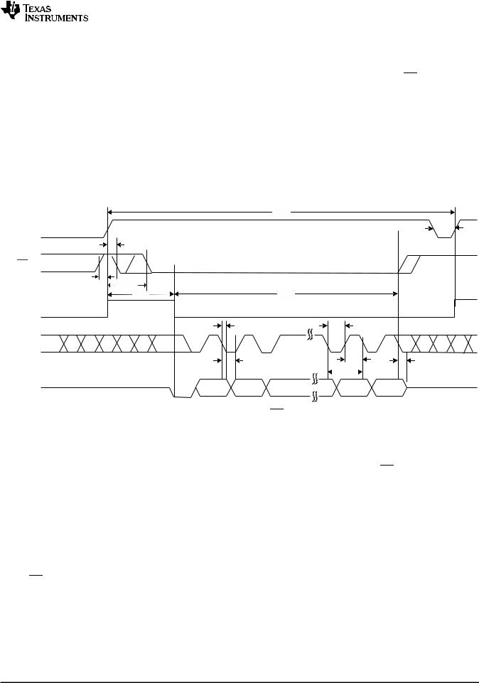
Unlike in the 3-wire interface option, SDI is controlled by the digital host and functions like CS. As shown in Figure 53, SDI goes to a high level before the CONVST rising edge. When SDI is high, the CONVST rising edge selects the CS mode, forces SDO to 3-state, samples the input signal, and the device enters the conversion phase.
In the 4-wire interface option, CONVST must be at a high level from the start of the conversion until all data bits are read. Conversion is done with the internal clock and continues regardless of the state of SDI. As a result, SDI (functioning as CS) can be toggled to select other devices on the board.
SDI must return low before the minimum conversion time (tcnv_min in the Timing Requirements table) elapses and must remain low until the end of the maximum conversion time. A low level on the SDI input at the end of a conversion ensures the device generates a busy indicator (low on SDO). For fast settling, a 10-kΩ pull-up resistor tied to +VBD is recommended to provide the necessary current to drive SDO low.
|
|
|
|
|
tcyc |
|
CNVST |
|
|
|
|
|
t6 |
|
|
t5 |
|
|
|
|
SDI ( CS ) |
|
|
|
|
|
|
|
t4 |
tcnv_min |
|
|
|
|
|
|
|
|
|
|
|
|
|
tcnv |
|
|
tacq |
|
Phase |
Acquisition |
Conversion |
|
|
Acquisition |
|
|
|
|
|
t2 |
tclkh |
|
SCLK |
|
1 |
2 |
3 |
16 |
17 |
|
|
|
|
t3 |
tclkl |
tdis |
SDO |
|
|
|
|
tclk |
|
|
|
|
|
|
|
|
|
|
|
D 15 |
D 14 |
D 1 |
D 0 |
Figure 53. Interface Timing Diagram: 4-Wire CS Mode With a Busy Indicator
When the conversion is complete, the device enters acquisition phase, powers down, forces SDO out of 3-state, and outputs a busy indicator bit (low level). The device outputs the MSB of the data on the first SCLK falling edge after the conversion is complete and continues to output the next lower data bits on every subsequent SCLK falling edge. SDO goes to 3-state after the 17th SCLK falling edge or when SDI (CS) is high, whichever occurs first.
Care must be taken so that CONVST and SDI are not both low at any time during the cycle.
9.4.3 Daisy-Chain Mode
Daisy-chain mode is selected if SDI is low at the time of the CONVST rising edge. This mode is useful to reduce wiring and hardware requirements (such as digital isolators in applications where multiple ADC devices are used). In this mode, all devices are connected in a chain (the SDO of one device is connected to the SDI of the next device) and data transfer is analogous to a shift register.
As in CS mode, this mode offers operation with or without a busy indicator. This section discusses these interface options in detail.
Copyright © 2014, Texas Instruments Incorporated |
Submit Documentation Feedback |
23 |
Product Folder Links: ADS8339

ADS8339
SBAS677A –JUNE 2014–REVISED OCTOBER 2014 |
www.ti.com |
Device Functional Modes (continued)
9.4.3.1 Daisy-Chain Mode Without a Busy Indicator
A connection diagram for this mode is shown in Figure 54. The SDI for device 1 is tied to ground and the SDO of device 1 goes to the SDI of device 2, and so on. The SDO of the last device in the chain goes to the digital host. CONVST for all devices in the chain are tied together. There is no CS signal in this mode.
|
|
|
|
CNV |
|
CONVST |
|
CONVST |
|
SDI |
SDO |
SDI |
SDO |
SDI |
|
SCLK |
|
SCLK |
|
|
|
|
|
CLK |
|
Device 1 |
|
Device 2 |
|
Digital Host
Figure 54. Connection Diagram: Daisy-Chain Mode Without a Busy Indicator (SDI = 0)
The device SDO is driven low when SDI low selects daisy-chain mode and the device samples the analog input and enters the conversion phase. SCLK must be low at the CONVST rising edge (as shown in Figure 55) so that the device does not generate a busy indicator at the end of the conversion. In this mode, CONVST remains high from the start of the conversion until all data bits are read. When started, the conversion continues regardless of the state of SCLK.
|
|
|
|
|
tcyc |
|
|
|
|
|
CONVST |
|
|
|
|
|
|
|
|
|
t6 |
|
|
tcnv |
|
|
|
|
tacq |
|
|
|
Phase |
Acquisition |
Conversion |
|
|
|
Acquisition |
|
|
|
|
|
t7 |
|
|
t2 |
tclkl |
|
|
|
|
|
SCLK |
|
|
1 |
2 |
15 |
16 |
17 |
18 |
31 |
32 |
|
t8 |
|
|
|
|
tclkh |
|
|
|
|
|
|
|
|
|
tclk |
|
|
|
|
|
SDO 1, SDI 2 |
|
|
#1-D15 |
#1-D14 |
#1-D1 |
#1-D0 |
|
|
|
|
|
|
|
|
t3 |
|
|
|
|
|
|
SDO 2 |
|
|
#2-D15 |
#2-D14 |
#2-D1 |
#2-D0 |
#1-D15 |
#1-D14 |
#1-D1 |
#1-D0 |
Figure 55. Interface Timing Diagram: Daisy-Chain Mode Without a Busy Indicator
At the end of the conversion, every device in the chain initiates an output of its conversion data starting with the MSB bit. Furthermore, the next lower data bit is output on every subsequent SCLK falling edge. While every device outputs its data on the SDO pin, each device also receives the previous device data on the SDI pin (other than device 1) and stores the data in the shift register. The device latches incoming data on every SCLK falling edge. The SDO of the first device in the chain goes low after the 16th SCLK falling edge. All subsequent devices in the chain output the stored data from the previous device in MSB-first format immediately following their own data word. 16 × N clocks must read data for N devices in the chain.
24 |
Submit Documentation Feedback |
Copyright © 2014, Texas Instruments Incorporated |
Product Folder Links: ADS8339
ADS8339
www.ti.com |
SBAS677A –JUNE 2014 –REVISED OCTOBER 2014 |
Device Functional Modes (continued)
9.4.3.2 Daisy-Chain Mode With a Busy Indicator
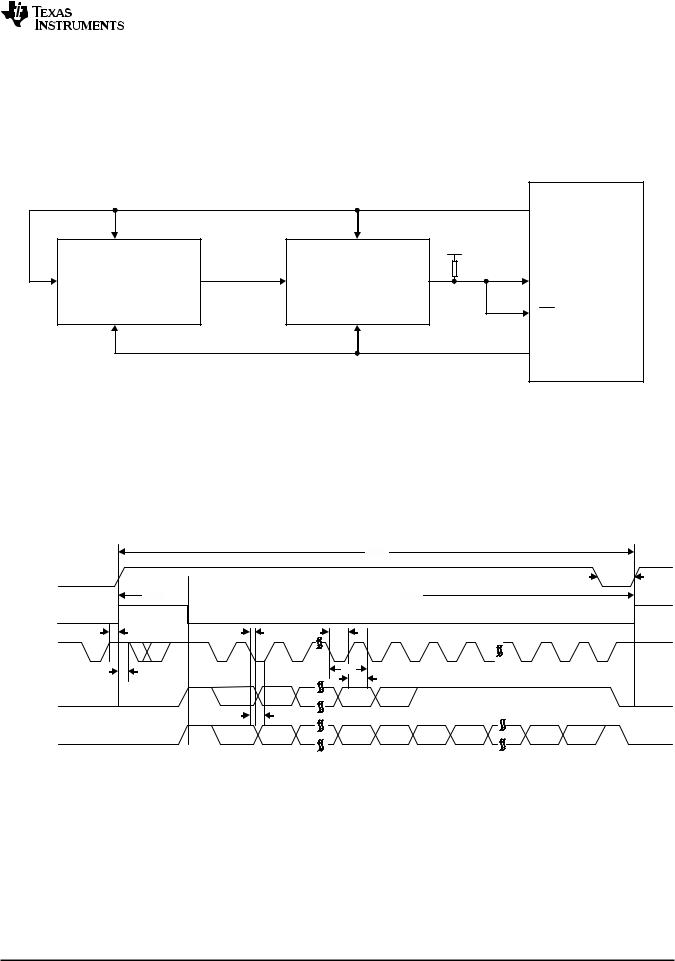
A connection diagram for this mode is shown in Figure 56. The SDI for device 1 is wired to its CONVST and the CONVST for all devices in the chain are wired together. The SDO of device 1 goes to the SDI of device 2, and so on. The SDO of the last device in the chain goes to the digital host. There is no CS signal in this mode.
|
|
|
|
CNV |
|
CONVST |
|
CONVST |
+VBD |
|
|
|
||
SDI |
SDO |
SDI |
SDO |
SDI |
|
SCLK |
|
SCLK |
IRQ |
|
|
|
|
|
|
|
|
|
CLK |
|
Device 1 |
|
Device 2 |
|
Digital Host
Figure 56. Connection Diagram: Daisy Chain Mode With a Busy Indicator (SDI = 0)
On the CONVST rising edge, all devices in the chain sample the analog input and enter the conversion phase. For the first device, SDI and CONVST are wired together and the setup time of SDI to the CONVST rising edge is adjusted so that the device still enters daisy-chain mode even though SDI and CONVST rise together. SCLK must be high at the CONVST rising edge (as shown in Figure 57) so that the device generates a busy indicator at the end of the conversion. In this mode, CONVST remains high from the start of the conversion until all data bits are read. When started, the conversion continues regardless of the state of SCLK.
tcyc
CONVST |
t6 |
tcnv 

 tacq
tacq
Phase |
Acquisition |
Conversion |
|
|
|
|
Acquisition |
|
|
|
|
|
t7 |
|
|
|
t2 |
tclkl |
|
|
|
|
|
SCLK |
|
|
1 |
2 |
3 |
16 |
17 |
18 |
19 |
32 |
33 |
|
t8 |
|
|
|
|
tclk |
tclkh |
|
|
|
|
|
|
|
|
|
|
|
|
|
|
||
|
|
|
|
|
|
|
|
|
|
|
|
SDO 1, SDI 2 |
|
|
|
#1-D15 |
#1-D14 |
#1-D1 |
#1-D0 |
|
|
|
|
|
|
|
|
|
t3 |
|
|
|
|
|
|
SDO 2 |
|
|
|
#2-D15 |
#2-D14 |
#2-D1 |
#2-D0 |
#1-D15 |
#1-D14 |
#1-D1 |
#1-D0 |
Figure 57. Interface Timing Diagram: Daisy Chain Mode With a Busy Indicator
At the end of the conversion, all devices in the chain generate busy indicators. On the first SCLK falling edge following the busy indicator bit, all devices in the chain output their conversion data starting with the MSB bit. Afterwards, the next lower data bit is output on every SCLK falling edge. While every device outputs its data on the SDO pin, each device also receives the previous device data on the SDI pin (except for device 1) and stores the data in the shift register. Each device latches incoming data on every SCLK falling edge. The SDO of the first device in the chain goes high after the 17th SCLK falling edge. All subsequent devices in the chain output the stored data from the pervious device in MSB-first format immediately following their own data word. 16 × N + 1 clock pulses are required to read data for N devices in the chain.
Copyright © 2014, Texas Instruments Incorporated |
Submit Documentation Feedback |
25 |
Product Folder Links: ADS8339