

бакМИТ_КП2015 / Компоненты по вариантам / АЦП / MAX1062
.pdf19-2203; Rev 1; 5/09
14-Bit, +5V, 200ksps ADC with 10µA Shutdown
General Description
The MAX1062 low-power, 14-bit analog-to-digital converter (ADC) features a successive approximation ADC, automatic power-down, fast 1.1µs wake-up, and a highspeed SPI™/QSPI™/MICROWIRE™-compatible interface. The MAX1062 operates with a single +5V analog supply and features a separate digital supply, allowing direct interfacing with 2.7V to 5.25V digital logic.
At the maximum sampling rate of 200ksps, the MAX1062 consumes typically 2.75mA. Power consumption is typically 13.75mW (AVDD = DVDD = 5V) at a 200ksps (max) sampling rate. AutoShutdown™ reduces supply current to 140µA at 10ksps and to less than 10µA at reduced sampling rates.
Excellent dynamic performance and low power, combined with ease of use and small package size (10-pin µMAX®) make the MAX1062 ideal for battery-powered and data-acquisition applications or for other circuits with demanding power consumption and space requirements.
Features
♦14-Bit Resolution, 1LSB DNL
♦+5V Single-Supply Operation
♦Adjustable Logic Level (2.7V to 5.25V)
♦Input Voltage Range: 0 to VREF
♦Internal Track/Hold, 4MHz Input Bandwidth
♦SPI/QSPI/MICROWIRE-Compatible Serial Interface
♦Small 10-Pin µMAX Package
♦Low Power
2.75mA at 200ksps 140µA at 10ksps
0.1µA in Power-Down Mode
MAX1062
|
Applications |
|
|
Ordering Information |
|||
Motor Control |
|
|
|
|
|
||
PART |
|
TEMP. |
PIN- |
INL |
|||
Industrial Process Control |
|
|
RANGE |
PACKAGE |
(LSB) |
||
|
|
||||||
Industrial I/O Modules |
MAX1062ACUB |
0°C to 70°C |
10 µMAX |
±1 |
|||
Data-Acquisition Systems |
|
MAX1062BCUB |
0°C to 70°C |
10 µMAX |
±2 |
||
|
MAX1062CCUB |
0°C to 70°C |
10 µMAX |
±3 |
|||
Thermocouple Measurements |
|
||||||
|
MAX1062AEUB |
-40°C to 85°C |
10 µMAX |
±1 |
|||
Accelerometer Measurements |
|
||||||
|
MAX1062BEUB |
-40°C to 85°C |
10 µMAX |
±2 |
|||
Portableand Battery-Powered Equipment |
|
||||||
|
MAX1062CEUB |
-40°C to 85°C |
10 µMAX |
±3 |
|||
|
|
|
|||||
|
|
|
|
|
|
|
|
Functional Diagram appears at end of data sheet.
SPI and QSPI are trademarks of Motorola, Inc.
MICROWIRE is a trademark of National Semiconductor Corp. AutoShutdown is a trademark of Maxim Integrated Products, Inc. µMAX is a registered trademark of Maxim Integrated Products, Inc.
Pin Configuration
TOP VIEW
REF |
1 |
10 |
AIN |
AVDD |
2 |
9 |
AGND |
AGND |
3 |
MAX1062 |
DVDD |
8 |
|||
CS |
4 |
7 |
DGND |
SCLK |
5 |
6 |
DOUT |
MAX
________________________________________________________________ Maxim Integrated Products 1
For pricing, delivery, and ordering information, please contact Maxim Direct at 1-888-629-4642, or visit Maxim’s website at www.maxim-ic.com

14-Bit, +5V, 200ksps ADC with 10µA Shutdown
MAX1062
ABSOLUTE MAXIMUM RATINGS
AVDD to AGND ........................................................ |
-0.3V to +6V |
Continuous Power Dissipation (TA = +70°C) |
|
|
DVDD to DGND........................................................ |
-0.3V to +6V |
10-Pin µMAX (derate 5.6mW/°C above +70°C) |
..........444mW |
|
DGND to AGND.................................................... |
-0.3V to +0.3V |
Operating Temperature Ranges |
|
|
AIN, REF to AGND ................................... |
-0.3V to (AVDD + 0.3V) |
MAX1062_CUB ................................................. |
|
0°C to +70°C |
SCLK, CS to DGND .................................................. |
-0.3V to +6V |
MAX1062_EUB .............................................. |
-40°C to +85°C |
|
DOUT to DGND ....................................... |
-0.3V to (DVDD + 0.3V) |
Maximum Junction Temperature ..................................... |
|
+150°C |
Maximum Current Into Any Pin ........................................... |
50mA |
Storage Temperature Range ............................. |
-65°C to +150°C |
|
|
|
Lead Temperature (soldering, 10s) ................................. |
|
+300°C |
Stresses beyond those listed under “Absolute Maximum Ratings” may cause permanent damage to the device. These are stress ratings only, and functional operation of the device at these or any other conditions beyond those indicated in the operational sections of the specifications is not implied. Exposure to absolute maximum rating conditions for extended periods may affect device reliability.
ELECTRICAL CHARACTERISTICS
(AVDD = DVDD = +4.75V to +5.25V, fSCLK = 4.8MHz (50% duty cycle), 24 clocks/conversion (200ksps), VREF = +4.096V, TA = TMIN to TMAX, unless otherwise noted. Typical values are at TA = +25°C.)
PARAMETER |
SYMBOL |
CONDITIONS |
MIN |
TYP |
MAX |
UNITS |
DC ACCURACY (NOTE 1) |
|
|
|
|
|
|
Resolution |
|
|
14 |
|
|
Bits |
|
|
|
|
|
|
|
|
|
MAX1062A |
|
|
±1 |
|
|
|
|
|
|
|
|
Relative Accuracy (Note 2) |
INL |
MAX1062B |
|
|
±2 |
LSB |
|
|
|
|
|
|
|
|
|
MAX1062C |
|
|
±3 |
|
Differential Nonlinearity |
DNL |
No missing codes over temperature |
|
±0.5 |
±1 |
LSB |
Transition Noise |
|
RMS noise |
|
±0.32 |
|
LSBRMS |
Offset Error |
|
|
|
0.2 |
1 |
mV |
|
|
|
|
|
|
|
Gain Error (Note 3) |
|
|
|
±0.002 |
±0.01 |
%FSR |
|
|
|
|
|
|
|
Offset Drift |
|
|
|
0.4 |
|
ppm/oC |
Gain Drift (Note 3) |
|
|
|
0.2 |
|
ppm/oC |
DYNAMIC SPECIFICATIONS (1kHz sine wave, 4.096Vp-p) (Note 1) |
|
|
|
|
||
|
|
|
|
|
|
|
Signal-to-Noise Plus Distortion |
SINAD |
|
81 |
84 |
|
dB |
Signal-to-Noise Ratio |
SNR |
|
82 |
84 |
|
dB |
|
|
|
|
|
|
|
Total Harmonic Distortion |
THD |
|
|
-99 |
-86 |
dB |
|
|
|
|
|
|
|
Spurious-Free Dynamic Range |
SFDR |
|
87 |
101 |
|
dB |
|
|
|
|
|
|
|
Full-Power Bandwidth |
|
-3dB point |
|
4 |
|
MHz |
|
|
|
|
|
|
|
Full-Linear Bandwidth |
|
SINAD > 81dB |
|
20 |
|
kHz |
CONVERSION RATE |
|
|
|
|
|
|
Conversion Time (Note 4) |
tCONV |
|
5 |
|
240 |
µs |
Serial Clock Frequency |
fSCLK |
|
0.1 |
|
4.8 |
MHz |
Aperture Delay |
|
|
|
15 |
|
ns |
|
|
|
|
|
|
|
Aperture Jitter |
|
|
|
<50 |
|
ps |
|
|
|
|
|
|
|
Sample Rate |
fS |
fSCLK / 24 |
|
|
200 |
ksps |
Track/Hold Acquisition Time |
tACQ |
|
1.1 |
|
|
µs |
2_______________________________________________________________________________________

14-Bit, +5V, 200ksps ADC with 10µA Shutdown
ELECTRICAL CHARACTERISTICS (continued)
(AVDD = DVDD = +4.75V to +5.25V, fSCLK = 4.8MHz (50% duty cycle), 24 clocks/conversion (200ksps), VREF = +4.096V, TA = TMIN to TMAX, unless otherwise noted. Typical values are at TA = +25°C.)
PARAMETER |
SYMBOL |
|
CONDITIONS |
MIN |
TYP |
MAX |
UNITS |
|
ANALOG INPUT (AIN) |
|
|
|
|
|
|
|
|
Input Range |
VAIN |
|
|
|
0 |
|
VREF |
V |
Input Capacitance |
CAIN |
|
|
|
|
40 |
|
pF |
EXTERNAL REFERENCE |
|
|
|
|
|
|
|
|
Input Voltage Range |
VREF |
|
|
|
3.8 |
|
AVDD |
V |
|
|
VREF = 4.096V, fSCLK = 4.8MHz |
|
100 |
|
|
||
Input Current |
IREF |
VREF = 4.096V, SCLK idle |
|
0.01 |
|
µA |
||
|
|
CS = DVDD, SCLK idle |
|
0.01 |
|
|
||
DIGITAL INPUTS (SCLK, CS) |
|
|
|
|
|
|
|
|
|
|
|
|
|
|
|
|
|
Input High Voltage |
VIH |
DVDD = +2.7V to +5.25V |
0.7 x |
|
|
V |
||
DVDD |
|
|||||||
|
|
|
|
|
|
|
||
|
|
|
|
|
|
|
|
|
Input Low Voltage |
VIL |
DVDD = +2.7V to +5.25V |
|
|
0.3 x |
V |
||
|
|
DVDD |
||||||
|
|
|
|
|
|
|
|
|
Input Leakage Current |
IIN |
VIN = 0 to DVDD |
|
±0.1 |
±1 |
µA |
||
Input Hysteresis |
VHYST |
|
|
|
|
0.2 |
|
V |
Input Capacitance |
CIN |
|
|
|
|
15 |
|
pF |
DIGITAL OUTPUT (DOUT) |
|
|
|
|
|
|
|
|
|
|
|
|
|
|
|
|
|
Output High Voltage |
VOH |
ISOURCE = 0.5mA, DVDD = +2.7V to +5.25V |
DVDD |
- |
|
V |
||
0.25V |
|
|
||||||
|
|
|
|
|
|
|
|
|
|
|
|
|
|
|
|
|
|
Output Low Voltage |
VOL |
ISINK = 10mA, DVDD = +4.75V to +5.25V |
|
|
0.7 |
V |
||
ISINK = 1.6mA, DVDD = +2.7V to +5.25V |
|
|
0.4 |
|||||
|
|
|
|
|
||||
Three-State Output Leakage |
IL |
CS = DVDD |
|
|
|
±0.1 |
±10 |
µA |
Current |
|
|
|
|||||
|
|
|
|
|
|
|
|
|
|
|
|
|
|
|
|
|
|
Three-State Output Capacitance |
COUT |
CS = DVDD |
|
|
|
15 |
|
pF |
POWER SUPPLIES |
|
|
|
|
|
|
|
|
Analog Supply |
AVDD |
|
|
|
4.75 |
|
5.25 |
V |
Digital Supply |
DVDD |
|
|
|
2.7 |
|
5.25 |
V |
|
|
|
|
200ksps |
|
2.75 |
3.25 |
|
|
|
|
|
|
|
|
|
|
Analog Supply Current |
IAVDD |
CS = DGND |
|
100ksps |
|
1.4 |
|
mA |
|
10ksps |
|
0.14 |
|
||||
|
|
|
|
|
|
|
||
|
|
|
|
1ksps |
|
0.014 |
|
|
|
|
CS = DGND, |
|
200ksps |
|
0.6 |
1.0 |
|
|
|
|
|
|
|
|
|
|
|
|
|
100ksps |
|
0.3 |
|
|
|
Digital Supply Current |
IDVDD |
DOUT = all |
|
|
|
mA |
||
|
10ksps |
|
0.03 |
|
||||
|
|
zeros |
|
|
|
|
||
|
|
|
|
|
|
|
|
|
|
|
|
1ksps |
|
0.003 |
|
|
|
|
|
|
|
|
|
|
||
|
|
|
|
|
|
|
|
|
MAX1062
_______________________________________________________________________________________ 3

MAX1062
14-Bit, +5V, 200ksps ADC with 10µA Shutdown
ELECTRICAL CHARACTERISTICS (continued)
(AVDD = DVDD = +4.75V to +5.25V, fSCLK = 4.8MHz (50% duty cycle), 24 clocks/conversion (200ksps), VREF = +4.096V, TA = TMIN to TMAX, unless otherwise noted. Typical values are at TA = +25°C.)
PARAMETER |
SYMBOL |
CONDITIONS |
MIN |
TYP |
MAX |
UNITS |
|
|
|
|
|
|
|
Shutdown Supply Current |
IAVDD + |
CS = DVDD, SCLK = idle |
|
0.1 |
10 |
µA |
IDVDD |
|
|||||
|
|
|
|
|
|
|
|
|
|
|
|
|
|
Power-Supply Rejection Ratio |
PSRR |
AVDD = DVDD = +4.75V to +5.25V, full-scale |
|
68 |
|
dB |
(Note 5) |
input |
|
|
|||
|
|
|
|
|
||
|
|
|
|
|
|
|
MAX1062 TIMING CHARACTERISTICS (Figures 1, 2, 3, and 6)
(AVDD = DVDD = +4.75V to +5.25V, fSCLK = 4.8MHz (50% duty cycle), 24 clocks/conversion (200ksps), VREF = +4.096V, TA = TMIN to TMAX, unless otherwise noted. Typical values are at TA = +25°C.)
PARAMETER |
SYMBOL |
CONDITIONS |
MIN |
TYP |
MAX |
UNITS |
|
|
|
|
|
|
|
Acquisition Time |
tACQ |
|
1.1 |
|
|
µs |
SCLK to DOUT Valid |
tDO |
CDOUT = 50pF |
|
|
50 |
ns |
CS Fall to DOUT Enable |
tDV |
CDOUT = 50pF |
|
|
80 |
ns |
CS Rise to DOUT Disable |
tTR |
CDOUT = 50pF |
|
|
80 |
ns |
CS Pulse Width |
tCSW |
|
50 |
|
|
ns |
CS Fall to SCLK Rise Setup |
tCSS |
|
100 |
|
|
ns |
CS Rise to SCLK Rise Hold |
tCSH |
|
|
|
0 |
ns |
SCLK High Pulse Width |
tCH |
|
65 |
|
|
ns |
SCLK Low Pulse Width |
tCL |
|
65 |
|
|
ns |
SCLK Period |
tCP |
|
208 |
|
|
ns |
|
|
|
|
|
|
|
(AVDD = +4.75V to +5.25V, DVDD = +2.7V to +5.25V, fSCLK = 4.8MHz (50% duty cycle), 24 clocks/conversion (200ksps), VREF = +4.096V, TA = TMIN to TMAX, unless otherwise noted. Typical values are at TA = +25°C.)
PARAMETER |
SYMBOL |
CONDITIONS |
MIN |
TYP |
MAX |
UNITS |
|
|
|
|
|
|
|
Acquisition Time |
tACQ |
|
1.1 |
|
|
µs |
SCLK to DOUT Valid |
tDO |
CDOUT = 50pF |
|
|
100 |
ns |
CS Fall to DOUT Enable |
tDV |
CDOUT = 50pF |
|
|
100 |
ns |
CS Rise to DOUT Disable |
tTR |
CDOUT = 50pF |
|
|
80 |
ns |
CS Pulse Width |
tCSW |
|
50 |
|
|
ns |
CS Fall to SCLK Rise Setup |
tCSS |
|
100 |
|
|
ns |
CS Rise to SCLK Rise Hold |
tCSH |
|
|
|
0 |
ns |
SCLK High Pulse Width |
tCH |
|
65 |
|
|
ns |
SCLK Low Pulse Width |
tCL |
|
65 |
|
|
ns |
SCLK Period |
tCP |
|
208 |
|
|
ns |
|
|
|
|
|
|
|
Note 1: AVDD = DVDD = +5V.
Note 2: Relative accuracy is the deviation of the analog value at any code from its theoretical value after the full-scale range has been calibrated.
Note 3: Offset and reference errors nulled.
Note 4: Conversion time is defined as the number of clock cycles multiplied by the clock period; clock has 50% duty cycle. Note 5: Defined as the change in positive full scale caused by a ±5% variation in the nominal supply voltage.
4_______________________________________________________________________________________

14-Bit, +5V, 200ksps ADC with 10µA Shutdown
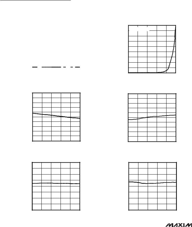
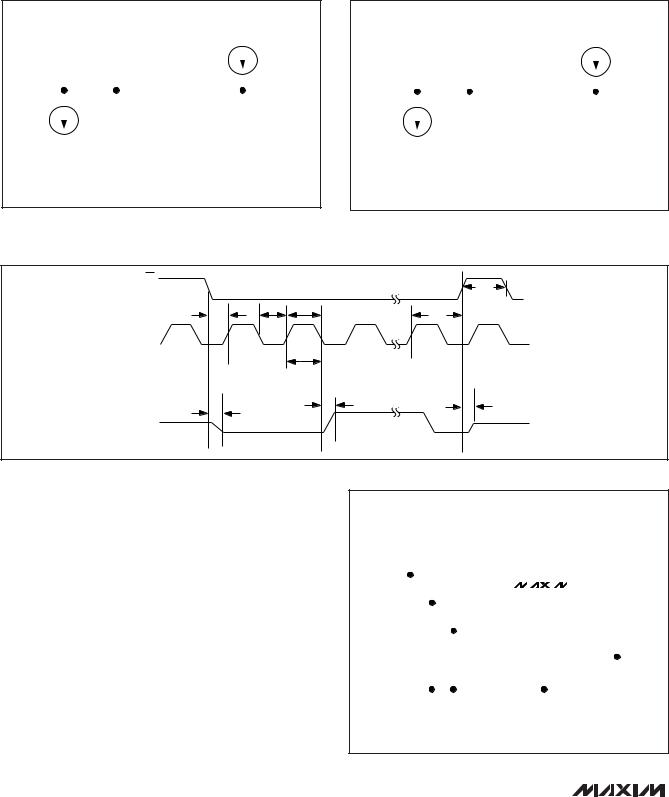
Typical Operating Characteristics
(AVDD = DVDD = +5V, fSCLK = 4.8MHz, CLOAD = 50pF, VREF = +4.096V, TA = 25°C, unless otherwise noted.)
INL vs. OUTPUT CODE |
DNL vs. OUTPUT CODE |
MAX1062 FFT |
INL (LSB)
1.0
0.8
0.6
0.4
0.2
0 -0.2 -0.4 -0.6 -0.8 -1.0
MAX1062 toc01
0 |
3276 |
6553 |
9830 |
13107 |
16384 |
OUTPUT CODE
DNL (LSB)
1.0
0.8
0.6
0.4
0.2
0 -0.2 -0.4 -0.6 -0.8 -1.0
MAX1062 toc02
0 |
3276 |
6553 |
9830 |
13107 |
16384 |
OUTPUT CODE
MAGNITUDE (dB)
0 |
|
|
toc03 |
|
|
||
|
|
|
|
-20 |
|
|
MAX1062 |
|
|
|
-40
-60
-80
-100
-120 |
-140
0 |
10 |
20 |
30 |
40 |
50 |
60 |
70 |
80 |
90 |
100 |
FREQUENCY (kHz)
SINAD VS. FREQUENCY |
SFDR VS. FREQUENCY |
THD VS. FREQUENCY |
|
100 |
|
|
toc04 |
|
110 |
|
90 |
|
|
|
100 |
|
|
|
|
MAX1062 |
|
||
|
80 |
|
|
|
90 |
|
|
70 |
|
|
|
|
80 |
|
|
|
|
|
70 |
|
(dB) |
60 |
|
|
|
(dB) |
|
|
|
|
60 |
|||
|
|
|
|
|||
SINAD |
50 |
|
|
|
SFDR |
|
|
|
|
50 |
|||
40 |
|
|
|
|||
|
|
|
40 |
|||
|
|
|
|
|
||
|
30 |
|
|
|
|
|
|
|
|
|
|
30 |
|
|
20 |
|
|
|
|
|
|
|
|
|
|
20 |
|
|
|
|
|
|
|
|
|
10 |
fSAMPLE = 200kHz |
|
|
|
10 |
|
0 |
|
|
|
|
0 |
|
0.1 |
1 |
10 |
100 |
|
|
|
|
FREQUENCY (kHz) |
|
|
|
|
|
|
|
toc05 |
0 |
|
|
toc06 |
|
|
|
-10 |
fSAMPLE = 200kHz |
|
||
|
|
|
MAX1062 |
|
MAX1062 |
||
|
|
|
-20 |
|
|
||
|
|
|
|
-30 |
|
|
|
|
|
|
(dB) |
-40 |
|
|
|
|
|
|
-50 |
|
|
|
|
|
|
|
THD |
-60 |
|
|
|
|
|
|
|
-70 |
|
|
|
|
|
|
|
-80 |
|
|
|
|
|
|
|
-90 |
|
|
|
|
fSAMPLE = 200kHz |
|
|
-100 |
|
|
|
|
|
|
-110 |
|
|
|
|
0.1 |
1 |
10 |
100 |
|
|
|
|
0.1 |
1 |
10 |
100 |
||||
|
FREQUENCY (kHz) |
|
|
FREQUENCY (kHz) |
|
||
|
|
|
SUPPLY CURRENT |
|
|
|
|
|
SUPPLY CURRENT |
|
|
|
SUPPLY CURRENT VS. TEMPERATURE |
|||||||
|
|
|
VS. CONVERSION RATE |
|
|
|
VS. SUPPLY VOLTAGE |
|
|
|||||||||||
|
10 |
|
|
|
|
toc07 |
|
3.5 |
|
|
|
|
toc08 |
|
3.5 |
|
|
|
|
toc09 |
|
|
|
|
|
|
|
|
|
|
|
|
|
|
|
|
|
|
|||
|
1 |
|
|
|
|
MAX1062 |
|
3.0 |
|
|
|
|
MAX1062 |
|
3.0 |
|
|
|
|
MAX1062 |
|
|
|
|
|
|
|
|
|
|
|
|
|
|
|
|
|
|
|||
(mA) |
|
|
|
|
|
(mA) |
|
|
|
|
|
|
(mA) |
|
|
|
|
|
|
|
|
|
|
|
|
|
2.5 |
|
|
|
|
|
2.5 |
|
|
|
|
|
|||
CURRENT |
|
|
|
|
|
|
CURRENT |
|
|
|
|
|
CURRENT |
|
|
|
|
|
||
0.1 |
|
|
|
|
|
2.0 |
|
|
|
|
|
2.0 |
|
|
|
|
|
|||
|
|
|
|
|
|
|
|
|
|
|
|
|
|
|
|
|
|
|||
|
|
|
|
|
|
|
|
|
|
|
|
|
|
|
|
|
|
|
||
SUPPLY |
0.01 |
|
|
|
|
|
SUPPLY |
1.5 |
|
|
|
|
|
SUPPLY |
1.5 |
|
|
|
|
|
|
|
|
|
|
|
|
|
|
|
|
|
|
|
|
|
|
||||
|
|
|
|
|
|
|
|
|
|
|
|
|
|
|
|
|
|
|
|
|
|
|
|
|
|
|
|
|
1.0 |
|
|
|
|
|
|
1.0 |
|
|
|
|
|
|
0.001 |
|
|
|
|
|
|
0.5 |
|
|
|
|
|
|
0.5 |
|
|
|
|
|
|
|
|
|
|
|
|
|
|
|
|
|
|
|
|
|
AVDD = DVDD= +5V |
|
|||
|
|
|
|
|
|
|
|
|
|
|
|
|
|
|
|
|
|
|
||
|
0.0001 |
|
|
|
|
|
|
0 |
|
|
|
|
|
|
0 |
|
|
|
|
|
|
0.01 |
0.1 |
1 |
10 |
100 |
1000 |
|
4.75 |
4.85 |
4.95 |
5.05 |
5.15 |
5.25 |
|
-40 |
-15 |
10 |
35 |
60 |
85 |
|
|
|
CONVERSION RATE (kHz) |
|
|
|
|
SUPPLY VOLTAGE (V) |
|
|
|
|
|
TEMPERATURE (°C) |
|
|
||||
MAX1062
_______________________________________________________________________________________ 5
14-Bit, +5V, 200ksps ADC with 10µA Shutdown
MAX1062
Typical Operating Characteristics (continued)
(AVDD = DVDD = +5V, fSCLK = 4.8MHz, CLOAD = 50pF, VREF = +4.096V, TA = 25°C, unless otherwise noted.)
SHUTDOWN SUPPLY CURRENT
VS. SUPPLY VOLTAGE
|
20 |
|
|
|
|
|
|
|
|
|
|
|
|
toc10 |
|
|
|
|
|
|
|
|
|
|
|
|
|
||
|
18 |
|
|
|
|
|
|
|
|
|
|
|
|
|
|
|
|
|
|
|
|
|
|
|
|
|
|
MAX1062 |
|
|
|
|
|
|
|
|
|
|
|
|
|
|
||
|
16 |
|
|
|
|
|
|
|
|
|
|
|
|
|
|
|
|
|
|
|
|
|
|
|
|
|
|
|
|
|
14 |
|
|
|
|
|
|
|
|
|
|
|
|
|
|
|
|
|
|
|
|
|
|
|
|
|
|
|
|
(nA) |
12 |
|
|
|
|
|
|
|
|
|
|
|
|
|
|
|
|
|
|
|
|
|
|
|
|
|
|
||
10 |
|
|
|
|
|
|
|
|
|
|
|
|
|
|
SHDN |
|
|
|
|
|
|
|
|
|
|
|
|
|
|
|
|
|
|
|
|
|
|
|
|
|
|
|
||
8 |
|
|
|
|
|
|
|
|
|
|
|
|
|
|
I |
|
|
|
|
|
|
|
|
|
|
|
|
|
|
|
6 |
|
|
|
|
|
|
|
|
|
|
|
|
|
|
|
|
|
|
|
|
|
|
|
|
|
|
|
|
|
4 |
|
|
|
|
|
|
|
|
|
|
|
|
|
|
|
|
|
|
|
|
|
|
|
|
|
|
|
|
|
2 |
|
|
|
|
|
|
|
|
|
|
|
|
|
|
|
|
|
|
|
|
|
|
|
|
|
|
|
|
|
|
|
|
|
|
|
|
|
|
|
|
|
|
|
|
0 |
|
|
|
|
|
|
|
|
|
|
|
|
|
|
|
|
|
|
|
|
|
|
|
|
|
|
|
|
|
4.75 |
4.85 |
4.95 |
5.05 |
|
5.15 |
|
5.25 |
||||||
SUPPLY VOLTAGE (V)
OFFSET ERROR
VS. ANALOG SUPPLY VOLTAGE
|
1000 |
|
|
|
|
toc12 |
|
800 |
|
|
|
|
|
|
|
|
|
|
MAX1062 |
|
|
600 |
|
|
|
|
|
|
|
|
|
|
|
|
V) |
400 |
|
|
|
|
|
( |
200 |
|
|
|
|
|
ERROR |
|
|
|
|
|
|
0 |
|
|
|
|
|
|
OFFSET |
-200 |
|
|
|
|
|
-400 |
|
|
|
|
|
|
|
|
|
|
|
|
|
|
-600 |
|
|
|
|
|
|
-800 |
|
|
|
|
|
|
-1000 |
|
|
|
|
|
|
4.75 |
4.85 |
4.95 |
5.05 |
5.15 |
5.25 |
SUPPLY VOLTAGE (V)
GAIN ERROR
VS. ANALOG SUPPLY VOLTAGE
|
0.020 |
|
|
|
|
toc14 |
|
|
|
|
|
|
|
|
0.015 |
|
|
|
|
MAX1062 |
|
|
|
|
|
|
|
|
0.010 |
|
|
|
|
|
(%) |
0.005 |
|
|
|
|
|
ERROR |
|
|
|
|
|
|
0 |
|
|
|
|
|
|
GAIN |
-0.005 |
|
|
|
|
|
|
-0.010 |
|
|
|
|
|
|
-0.015 |
|
|
|
|
|
|
-0.020 |
|
|
|
|
|
|
4.75 |
4.85 |
4.95 |
5.05 |
5.15 |
5.25 |
SUPPLY VOLTAGE (V)
SHUTDOWN SUPPLY CURRENT
VS. TEMPERATURE
|
450 |
|
|
|
|
toc11 |
|
400 |
AVDD = DVDD = +5V |
|
|
||
|
|
|
MAX1062 |
|||
|
|
|
|
|
||
|
350 |
|
|
|
|
|
|
|
|
|
|
|
|
|
300 |
|
|
|
|
|
(nA) |
250 |
|
|
|
|
|
SHDN |
200 |
|
|
|
|
|
I |
|
|
|
|
|
|
|
150 |
|
|
|
|
|
|
100 |
|
|
|
|
|
|
50 |
|
|
|
|
|
|
0 |
|
|
|
|
|
|
-40 |
-15 |
10 |
35 |
60 |
85 |
|
|
|
TEMPERATURE (°C) |
|
|
|
OFFSET ERROR VS. TEMPERATURE
|
1000 |
|
|
|
|
toc13 |
|
800 |
|
|
|
|
|
|
|
|
|
|
MAX1062 |
|
|
600 |
|
|
|
|
|
|
|
|
|
|
|
|
V) |
400 |
|
|
|
|
|
( |
200 |
|
|
|
|
|
ERROR |
|
|
|
|
|
|
0 |
|
|
|
|
|
|
OFFSET |
-200 |
|
|
|
|
|
-400 |
|
|
|
|
|
|
|
|
|
|
|
|
|
|
-600 |
|
|
|
|
|
|
-800 |
|
|
|
|
|
|
-1000 |
|
|
|
|
|
|
-40 |
-15 |
10 |
35 |
60 |
85 |
TEMPERATURE (°C)
GAIN ERROR VS. TEMPERATURE
|
0.020 |
|
|
|
|
toc15 |
|
|
|
|
|
|
|
|
0.015 |
|
|
|
|
MAX1062 |
|
|
|
|
|
|
|
|
0.010 |
|
|
|
|
|
(%) |
0.005 |
|
|
|
|
|
ERROR |
|
|
|
|
|
|
0 |
|
|
|
|
|
|
GAIN |
-0.005 |
|
|
|
|
|
|
-0.010 |
|
|
|
|
|
|
-0.015 |
|
|
|
|
|
|
-0.020 |
|
|
|
|
|
|
-40 |
-15 |
10 |
35 |
60 |
85 |
TEMPERATURE (°C)
6_______________________________________________________________________________________

14-Bit, +5V, 200ksps ADC with 10µA Shutdown
|
|
|
Pin Description |
|
|
|
|
||
PIN |
NAME |
FUNCTION |
||
|
|
|
||
1 |
REF |
External Reference Voltage Input. Sets the analog voltage range. Bypass to AGND with a 4.7µF |
||
capacitor. |
||||
|
|
|||
|
|
|
||
2 |
AVDD |
Analog +5V Supply Voltage. Bypass to AGND (pin 3) with a 0.1µF capacitor. |
||
3, 9 |
AGND |
Analog Ground. Connect pins 3 and 9 together. Place star ground at pin 3. |
||
|
|
Active Low Chip Select Input. Forcing CS high places the MAX1062 in shutdown with a typical |
||
4 |
CS |
current of 0.1µA. A high-to-low transition on CS activates normal operating mode and initiates a |
||
|
|
conversion. |
||
|
|
|
||
5 |
SCLK |
Serial Clock Input. SCLK drives the conversion process and clocks out data at data rates up to |
||
4.8MHz. |
||||
|
|
|||
|
|
|
||
6 |
DOUT |
Serial Data Output. Data changes state on SCLK’s falling edge. DOUT is high impedance when CS |
||
is high. |
||||
|
|
|||
|
|
|
||
7 |
DGND |
Digital Ground |
||
|
|
|
||
8 |
DVDD |
Digital Supply Voltage. Bypass to DGND with a 0.1µF capacitor. |
||
10 |
AIN |
Analog Input |
||
|
|
|
|
|
Detailed Description
The MAX1062 includes an input track-and-hold (T/H) and successive-approximation register (SAR) circuitry to convert an analog input signal to a digital 14-bit output. Figure 4 shows the MAX1062 in its simplest configuration. The serial interface requires only three digital lines (SCLK, CS, and DOUT) and provides an easy interface to microprocessors (µPs).
The MAX1062 has two power modes: normal and shutdown. Driving CS high places the MAX1062 in shutdown, reducing the supply current to 0.1µA (typ), while pulling CS low places the MAX1062 in normal operating mode. Falling edges on CS initiate conversions that are driven by SCLK. The conversion result is available at DOUT in unipolar serial format. The serial data stream consists of eight zeros followed by the data bits (MSB first). Figure 3 shows the interface-timing diagram.
Analog Input
Figure 5 illustrates the input sampling architecture of the ADC. The voltage applied at REF sets the full-scale input voltage.
Track-and-Hold (T/H)
In track mode, the analog signal is acquired on the internal hold capacitor. In hold mode, the T/H switches open and the capacitive DAC samples the analog input.
During the acquisition, the analog input (AIN) charges capacitor CDAC. The acquisition interval ends on the falling edge of the sixth clock cycle (Figure 6). At this instant, the T/H switches open. The retained charge on CDAC represents a sample of the input.
In hold mode, the capacitive digital-to-analog converter (DAC) adjusts during the remainder of the conversion cycle to restore node ZERO to zero within the limits of 14-bit resolution. At the end of the conversion, force CS high and then low to reset the input side of the CDAC switches back to AIN, and charge CDAC to the input signal again.
The time required for the T/H to acquire an input signal is a function of how quickly its input capacitance is charged. If the input signal’s source impedance is high, the acquisition time lengthens and more time must be allowed between conversions. The acquisition time (tACQ) is the maximum time the device takes to acquire the signal. Use the following formula to calculate acquisition time:
tACQ = 11(RS + RIN) x 35pF
where RIN = 800Ω, RS = the input signal’s source impedance, and tACQ is never less than 1.1µs. A source impedance less than 1kΩ does not significantly affect the ADC’s performance.
To improve the input signal bandwidth under AC conditions, drive AIN with a wideband buffer (>4MHz) that can drive the ADC’s input capacitance and settle quickly.
MAX1062
_______________________________________________________________________________________ 7
14-Bit, +5V, 200ksps ADC with 10µA Shutdown
MAX1062
|
|
|
|
|
|
|
|
|
|
|
|
|
|
|
|
|
|
|
|
VDD |
||||||||
|
|
|
|
|
|
|
|
|
|
|
|
|
|
|
|
|
|
|
|
|
|
|
|
|
|
|
|
|
|
|
|
|
|
|
|
|
|
|
|
|
|
|
|
|
|
1mA |
|
|
|
|
|
|
|||||
|
|
|
|
|
|
|
|
|
|
|
|
|
|
|
|
|
|
|
|
|
|
|
||||||
|
|
|
|
|
|
|
|
|
|
|
|
|
|
|
|
|
|
|||||||||||
DOUT |
|
|
|
|
|
|
|
|
|
|
|
|
|
|
DOUT |
|
|
|
|
|
|
|
|
|
|
|
||
|
|
|
|
|
|
|
|
|
|
|
|
|
|
|
|
|
|
|
|
|
|
|
||||||
|
|
|
|
|
|
|
|
|
|
|
|
|
|
|
|
|
|
|
|
|||||||||
1mA |
|
|
|
|
|
|
|
|
|
|
|
CLOAD = 50pF |
|
|
|
|
|
|
|
|
|
|
CLOAD = 50pF |
|||||
|
|
|
|
|
|
|
|
|
|
|
|
|
|
|
|
|
|
|
|
|
||||||||
|
|
|
|
|
|
|
|
|
|
|
|
|
|
|
|
|
|
|
|
|
||||||||
|
|
|
|
|
|
|
|
DGND |
|
|
|
|
|
|
|
|
|
|
|
|
|
|
|
|
|
|
DGND |
|
|
|
|
|
|
|
|
|
|
|
|
|
|
|
|
|
|
|
|
|
|
|
|
|
|||||
|
|
|
|
|
|
|
|
|
|
|
|
|
|
|
|
|
|
|
|
|||||||||
|
|
|
|
|
|
|
|
|
|
|
|
|
|
|
|
|
||||||||||||
|
|
|
|
|
|
|
a) VOL TO VOH |
b) HIGH-Z TO VOL AND VOH TO VOL |
||||||||||||||||||||
Figure 1. Load Circuits for DOUT Enable Time and SCLK to DOUT Delay Time
|
|
|
|
|
|
|
|
|
|
|
|
|
|
|
|
|
|
|
|
VDD |
||||||||
|
|
|
|
|
|
|
|
|
|
|
|
|
|
|
|
|
|
|
|
|
|
|
|
|
|
|
|
|
DOUT |
|
|
|
|
|
|
|
|
|
|
|
|
|
|
|
|
1mA |
|
|
|
|
|
|
|||||
|
|
|
|
|
|
|
|
|
|
|
|
|
|
|
|
|
|
|
|
|
|
|||||||
|
|
|
|
|
|
|
|
|
|
|
|
|
|
|
|
|
||||||||||||
|
|
|
|
|
|
|
|
|
|
|
|
|
|
DOUT |
|
|
|
|
|
|
|
|
|
|
|
|||
|
|
|
|
|
|
|
|
|
|
|
|
|
|
|
|
|
|
|
|
|
|
|
||||||
|
|
|
|
|
|
|
|
|
|
|
|
|
|
|
|
|
|
|
|
|||||||||
1mA |
|
|
|
|
|
|
|
|
|
|
|
CLOAD = 50pF |
|
|
|
|
|
|
|
|
|
|
CLOAD = 50pF |
|||||
|
|
|
|
|
|
|
|
|
|
|
|
|
|
|
|
|
|
|
|
|
||||||||
|
|
|
|
|
|
|
|
|
|
|
|
|
|
|
|
|
|
|
|
|
||||||||
|
|
|
|
|
|
|
|
DGND |
|
|
|
|
|
|
|
|
|
|
|
|
|
|
|
|
|
|
DGND |
|
|
|
|
|
|
|
|
|
|
|
|
|
|
|
|
|
|
|
|
|
|
|
|
|
|||||
|
|
|
|
|
|
|
|
|
|
|
|
|
|
|
|
|
|
|
|
|||||||||
|
|
|
|
|
|
|
|
|
|
|
|
|
|
|
|
|
||||||||||||
|
|
|
|
|
|
a) VOH TO HIGH-Z |
b) VOL TO HIGH-Z |
|||||||||||||||||||||
Figure 2. Load Circuits for DOUT Disable Time
CS
|
|
tCSW |
tCL |
tCH |
tCSH |
tCSS |
|
|
SCLK |
|
|
|
tCP |
|
tDV |
tDO |
tTR |
|
|
DOUT
Figure 3. Detailed Serial Interface Timing
Input Bandwidth
The ADC’s input tracking circuitry has a 4MHz smallsignal bandwidth, so it is possible to digitize highspeed transient events and measure periodic signals with bandwidths exceeding the ADC’s sampling rate by using undersampling techniques. To avoid aliasing of unwanted high-frequency signals into the frequency band of interest, use antialias filtering.
Analog Input Protection
Internal protection diodes, which clamp the analog input to AVDD and/or AGND, allow the input to swing from AGND - 0.3V to AVDD + 0.3V, without damaging the device.
If the analog input exceeds 300mV beyond the supplies, limit the input current to 10mA.
AIN |
|
|
|
|
|
|
|
|
|
|
|
|
|
|
|
|
|
|
|
|
|
|
|
|
|
|
|
|
|
|
|
|
|
|
|
|
AIN |
|
|
|
|
|
|
|
|
CS |
|
CS |
|||||
|
|
|
|
|
|
|
|
|
|
|
|
|
|
|
|
|
|
|
||||||||
VREF |
|
|
|
|
|
|
|
|
|
|
REF |
|
|
|
|
|
|
|
|
SCLK |
|
SCLK |
||||
|
|
|
|
|
|
|
|
|
|
|
|
|
|
|
|
|
|
|
||||||||
|
|
|
|
|
|
|
|
|
|
|
|
|
|
|
|
|
|
DOUT |
|
DOUT |
||||||
|
|
|
|
4.7 F |
|
|
|
|
|
|
|
|
|
|
|
|
|
|
|
|
||||||
+5V |
|
AVDD |
MAX1062 |
|
|
|
|
|||||||||||||||||||
|
|
|
|
|
|
|
|
|
|
|
|
|
|
|||||||||||||
|
|
|
|
|
|
0.1 F |
|
|
|
|
|
|
|
|
|
|
|
|
|
|
|
|||||
+5V |
|
|
|
|
|
|
DVDD |
|
|
|
|
|
|
|
|
AGND |
|
|
|
|
||||||
|
|
|
|
|
|
|
|
|
|
|
|
|
|
|
|
|
|
|||||||||
|
|
|
|
|
|
|
|
|
|
|
|
|
|
|
|
|
|
|
|
|
|
|||||
|
|
|
|
|
|
|
|
|
|
|
|
|
|
|
|
|
|
|
|
|
|
|||||
|
|
|
|
|
|
|
|
|
|
|
|
|
|
|
|
|
|
|
|
|
|
|
|
|||
|
|
|
|
|
|
|
|
|
|
0.1 F |
|
|
|
|
|
|
|
|
|
DGND |
|
|
|
|
||
|
|
|
|
|
|
|
|
|
|
|
|
|
|
|
|
|
|
|
|
|
|
|
||||
|
|
|
|
|
|
|
|
|
|
|
|
|
|
|
|
|
|
|
|
|
|
|
|
|
|
|
|
|
|
|
|
|
|
|
|
|
|
|
|
|
|
|
|
|
|
|
|
|
|
|
|
|
|
|
|
|
|
|
|
|
|
|
|
|
|
|
|
|
|
|
|
|
GND |
|
|
|
||||
|
|
|
|
|
|
|
|
|
|
|
|
|
|
|
|
|
|
|
|
|
|
|||||
|
|
|
|
|
|
|
|
|
|
|
|
|
|
|
|
|
|
|
|
|
|
|||||
Figure 4. Typical Operating Circuit
8_______________________________________________________________________________________

14-Bit, +5V, 200ksps ADC with 10µA Shutdown
Digital Interface
Initialization after Power-Up and Starting a Conversion
The digital interface consists of two inputs, SCLK and CS, and one output, DOUT. A logic high on CS places the MAX1062 in shutdown (autoshutdown) and places DOUT in a high-impedance state. A logic low on CS places the MAX1062 in the fully powered mode.
To start a conversion, pull CS low. A falling edge on CS initiates an acquisition. SCLK drives the A/D conversion and shifts out the conversion results (MSB first) at DOUT.
Timing and Control
Conversion-start and data-read operations are controlled by the CS and SCLK digital inputs (Figures 6 and 7). Ensure that the duty cycle on SCLK is between 40% and 60% at 4.8MHz (the maximum clock frequency). For lower clock frequencies, ensure that the minimum high and low times are at least 65ns. Conversions with SCLK rates less than 100kHz may result in reduced accuracy due to leakage.
Note: Coupling between SCLK and the analog inputs (AIN and REF) may result in an offset. Variations in frequency, duty cycle, or other aspects of the clock signal’s shape result in changing offset.
A CS falling edge initiates an acquisition sequence. The analog input is stored in the capacitive DAC, DOUT changes from high impedance to logic low, and the ADC begins to convert after the sixth clock cycle. SCLK drives the conversion process and shifts out the conversion result on DOUT.
|
REF |
|
|
MAX1062 |
|
AIN |
TRACK |
CAPACITIVE DAC |
|
||
|
ZERO |
||||
|
|
|
|||
CSWITCH |
HOLD |
CDAC 32pF |
|
||
3pF |
RIN |
||||
|
|
||||
|
GND |
|
800Ω |
||
|
|
HOLD |
TRACK |
||
|
|
|
|||
|
|
|
|
||
|
|
|
|
AUTOZERO |
|
|
|
|
|
RAIL |
Figure 5. Equivalent Input Circuit
SCLK begins shifting out the data (MSB first) after the falling edge of the 8th SCLK pulse. Twenty-four falling clock edges are needed to shift out the eight leading zeros, 14 data bits, and 2 sub-bits (S1 and S0). Extra clock pulses occurring after the conversion result has been clocked out, and prior to the rising edge of CS, produce trailing zeros at DOUT and have no effect on the converter operation.
Force CS high after reading the conversion’s LSB to reset the internal registers and place the MAX1062 in shutdown. For maximum throughput, force CS low again to initiate the next conversion immediately after the specified minimum time (tCSW).
Note: Forcing CS high in the middle of a conversion immediately aborts the conversion and places the MAX1062 in shutdown.
CS |
|
|
|
|
|
|
|
|
|
|
|
|
|
|
|
|
|
|
|
SCLK |
1 |
4 |
6 |
8 |
|
|
12 |
|
|
|
16 |
|
|
|
20 |
|
|
|
24 |
|
tCSS |
tCH |
tCL |
|
|
|
|
|
|
|
|
|
|
|
|
|
|
|
tCSH |
DOUT |
|
|
|
|
|
|
|
|
|
|
|
|
|
|
|
|
|
||
|
|
D13 |
D12 |
D11 |
D10 |
D9 |
D8 |
D7 |
D6 |
D5 |
D4 |
D3 |
D2 |
D1 |
D0 |
S1 |
S0 |
||
|
tACQ |
|
|||||||||||||||||
tDN |
|
|
tDO |
|
|
|
|
|
|
|
|
|
|
|
|
|
|
tTR |
|
|
|
|
|
|
|
|
|
|
|
|
|
|
|
|
|
|
|
|
Figure 6. External Timing Diagram
_______________________________________________________________________________________ 9
14-Bit, +5V, 200ksps ADC with 10µA Shutdown
MAX1062
COMPLETE CONVERSION SEQUENCE
CS
DOUT
CONVERSION 0 |
|
CONVERSION 1 |
POWERED UP |
POWERED DOWN |
POWERED UP |
Figure 7. Shutdown Sequence
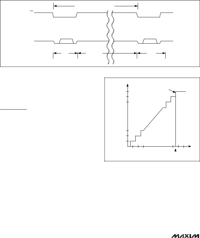
Output Coding and
Transfer Function
The data output from the MAX1062 is binary and Figure 8 depicts the nominal transfer function. Code transitions occur halfway between successive-integer LSB values (VREF = 4.096V and 1LSB = 250µV or 4.096V/16384).
Applications Information
External Reference
The MAX1062 requires an external reference with a voltage range between 3.8V and AVDD. Connect the external reference directly to REF. Bypass REF to AGND (pin 3) with a 4.7µF capacitor. When not using a low ESR bypass capacitor, use a 0.1µF ceramic capacitor in parallel with the 4.7µF capacitor. Noise on the reference degrades conversion accuracy.
The input impedance at REF is 40kΩ for DC currents. During a conversion the external reference at REF must deliver 100µA of DC load current and have an output impedance of 10Ω or less.
For optimal performance, buffer the reference through an op amp and bypass the REF input. Consider the MAX1062’s equivalent input noise (80µVRMS) when choosing a reference.
Input Buffer
Most applications require an input buffer amplifier to achieve 14-bit accuracy. If the input signal is multiplexed, switch the input channel immediately after acquisition, rather than near the end of or after a conversion (Figure 9). This allows the maximum time for the input buffer amplifier to respond to a large step change in the input signal. The input amplifier must have a slew rate of at least 2V/µs to complete the required output voltage change before the beginning of the acquisition time.
OUTPUT CODE
FULL-SCALE 11 . . . 111 TRANSITION
11 . . . 110
11 . . . 101
FS = VREF
1LSB = VREF 16384
00 . . . 011
00 . . . 010
00 . . . 001
00 . . . 000
0 1 2 |
3 |
|
FS |
|
|
|
|
|
INPUT VOLTAGE (LSB) |
FS - 3/2LSB |
|
Figure 8. Unipolar Transfer Function, Full Scale (FS) = VREF, Zero Scale (ZS) = GND
At the beginning of the acquisition, the internal sampling capacitor array connects to AIN (the amplifier output), causing some output disturbance. Ensure that the sampled voltage has settled before the end of the acquisition time.
Digital Noise
Digital noise can couple to AIN and REF. The conversion clock (SCLK) and other digital signals active during input acquisition contribute noise to the conversion result. Noise signals synchronous with the sampling interval result in an effective input offset. Asynchronous signals produce random noise on the input, whose
10 ______________________________________________________________________________________