

бакМИТ_КП2015 / Компоненты по вариантам / АЦП / MAX1062
.pdf14-Bit, +5V, 200ksps ADC with 10µA Shutdown |
|
|||
IN1 |
A0 |
A1 |
|
MAX1062 |
|
|
|
||
IN2 |
4-TO-1 |
|
|
|
|
MUX |
|
MAX1062 |
|
|
|
|
||
IN3 |
|
|
AIN |
|
IN4 |
|
OUT |
|
|
|
|
|
||
|
|
CS |
|
|
CLK |
|
|
|
|
|
|
CONVERSION |
ACQUISITION |
|
CS |
|
|
|
|
A0 |
|
|
|
|
A1 |
|
|
|
|
|
|
|
CHANGE MUX INPUT HERE |
|
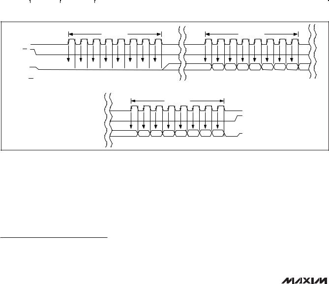
Figure 9. Change Multiplexer Input Near Beginning of Conversion to Allow Time for Slewing and Settling
high-frequency components may be aliased into the frequency band of interest. Minimize noise by presenting a low impedance (at the frequencies contained in the noise signal) at the inputs. This requires bypassing AIN to AGND, or buffering the input with an amplifier that has a small-signal bandwidth of several MHz, or preferably both. AIN has about 4MHz of bandwidth.
Distortion
Avoid degrading dynamic performance by choosing an amplifier with distortion much less than the MAX1062’s total harmonic distortion (THD = -99dB at 1kHz) at frequencies of interest. If the chosen amplifier has insufficient common-mode rejection, which results in degraded THD performance, use the inverting configuration (positive input grounded) to eliminate errors from this source. Low temperature-coefficient, gain-setting resistors reduce linearity errors caused by resistance changes due to self-heating. To reduce linearity errors due to finite amplifier gain, use amplifier circuits with sufficient loop gain at the frequencies of interest.
DC Accuracy
To improve DC accuracy, choose a buffer with an offset much less than the MAX1062’s offset (1mV (max) for +5V supply), or whose offset can be trimmed while maintaining stability over the required temperature range.
Serial Interfaces
The MAX1062’s interface is fully compatible with SPI, QSPI, and MICROWIRE standard serial interfaces.
If a serial interface is available, establish the CPU’s serial interface as master, so that the CPU generates the serial clock for the MAX1062. Select a clock frequency between 100kHz and 4.8MHz:
1)Use a general-purpose I/O line on the CPU to pull CS low.
2)Activate SCLK for a minimum of 24 clock cycles. The serial data stream of eight leading zeros fol-
lowed by the MSB of the conversion result begins at the falling edge of CS. DOUT transitions on SCLK’s falling edge and the output is available in MSB-first
______________________________________________________________________________________ 11

14-Bit, +5V, 200ksps ADC with 10µA Shutdown
MAX1062
format. Observe the SCLK to DOUT valid timing characteristic. Clock data into the µP on SCLK’s rising edge.
3)Pull CS high at or after the 24th falling clock edge. If CS remains low, trailing zeros are clocked out after the 2 sub-bits, S1 and S0.
4)With CS high, wait at least 50ns (tCSW) before starting a new conversion by pulling CS low. A conversion can be aborted by pulling CS high before the conversion ends. Wait at least 50ns before starting a new conversion.
Data can be output in three 8-bit sequences or continuously. The bytes contain the results of the conversion padded with eight leading zeros before the MSB. If the serial clock has not been idled after the sub-bits (S1 and S0) and CS has been kept low, DOUT sends trailing zeros.
SPI and MICROWIRE Interfaces
When using the SPI (Figure 10a) or MICROWIRE (Figure 10b) interfaces, set CPOL = 0 and CPHA = 0. Conversion begins with a falling edge on CS (Figure 10c). Three consecutive 8-bit readings are necessary to obtain the entire 14-bit result from the ADC. DOUT data transitions on the serial clock’s falling edge. The first 8-bit data stream contains all leading zeros. The second 8-bit data stream contains the MSB through D6. The third 8-bit data stream contains D5 through D0 followed by S1 and S0.
QSPI Interface
Using the high-speed QSPI interface with CPOL = 0 and CPHA = 0, the MAX1062 supports a maximum fSCLK of 4.8MHz. Figure 11a shows the MAX1062 connected to a QSPI master and Figure 11b shows the associated interface timing.
I/O |
CS |
SCK |
SCLK |
MISO |
DOUT |
SPI |
VDD |
|
MAX1062 |
SS |
|
Figure 10a. SPI Connections
I/O |
CS |
SK |
SCLK |
SI |
DOUT |
MICROWIRE |
|
|
MAX1067 |
|
MAX1068 |
Figure 10b. MICROWIRE Connections
|
|
|
|
1ST BYTE READ |
|
|
|
|
|
|
|
|
|
2ND BYTE READ |
|
|
|
|
||
SCLK |
|
1 |
|
|
4 |
|
6 |
8 |
|
|
|
|
|
|
12 |
|
|
|
16 |
|
|
|
|
|
|
|
|
|
|
|
|
|
|
|
|
|
|
|
|
|
|
CS |
|
|
|
|
|
|
|
|
|
|
|
|
|
|
|
|
|
|
|
|
DOUT* |
0 |
0 |
0 |
0 |
0 |
0 |
0 |
0 |
|
|
|
D13 |
D12 |
D11 |
D10 |
D9 |
D8 |
D7 |
D6 |
D5 |
|
|
|
|
|
|
|
|
|
|
|
||||||||||
|
|
|
|
|
|
|
|
|
|
|
|
MSB |
|
|
|
|
|
|
|
|
*WHEN CS IS HIGH, DOUT = HIGH-Z |
|
|
|
|
|
|
|
|
|
|
|
|
|
|
|
|
|
|
|
|
|
|
|
|
|
|
|
|
|
3RD BYTE READ |
|
|
|
|
|
|
|
|
|
|
|
|
|
|
|
|
|
|
|
|
20 |
|
|
|
24 |
|
|
|
|
|
|
|
|
|
|
|
|
|
D5 |
D4 |
D3 |
D2 |
D1 |
D0 |
S1 |
S0 |
|
HIGH-Z |
|
|
|
|
|
|
|
|
|
|
|
|
|
|
|
|
|
|
||||||||
|
|
|
|
|
|
|
|
|
|
|
LSB |
|
|
|
|
|
|
|
|
|
Figure 10c. SPI/MICROWIRE Interface Timing Sequence (CPOL = CPHA =0)
12 ______________________________________________________________________________________
14-Bit, +5V, 200ksps ADC with 10µA Shutdown
CS |
|
|
|
CS |
|
|
|
|
|
|
|||
SCK |
|
|
|
SCLK |
|
|
|
|
|
|
|||
MISO |
|
|
|
DOUT |
|
|
|
|
|
|
|
||
QSPI |
|
VDD |
|
|
||
|
|
|
|
|
|
|
MAX1062
SS
Figure 11a. QSPI Connections
SCLK |
1 |
4 |
6 |
8 |
|
|
12 |
|
|
|
16 |
|
|
|
20 |
|
|
|
24 |
CS |
|
|
|
|
|
|
|
|
|
|
|
|
|
|
|
|
|
|
|
|
|
|
END OF |
|
|
|
|
|
|
|
|
|
|
|
|
|
|
|
HIGH-Z |
DOUT* |
|
ACQUISITION |
D13 |
D12 |
D11 |
D10 |
D9 |
D8 |
D7 |
D6 |
D5 |
D4 |
D3 |
D2 |
D1 |
D0 |
S1 |
||
|
S0 |
||||||||||||||||||
*WHEN CS IS HIGH, DOUT = HIGH-Z |
|
|
MSB |
|
|
|
|
|
|
|
|
|
|
|
|
LSB |
|
|
|
|
|
|
|
|
|
|
|
|
|
|
|
|
|
|
|
|
|
||
Figure 11b. QSPI Interface Timing Sequence (CPOL = CPHA = 0)
VDD |
VDD |
SCLK |
SCK |
DOUT |
SDI |
CS |
I/O |
|
PIC16/17 |
MAX1062 |
|
GND |
|
Figure 12a. SPI Interface Connection for a PIC16/PIC17
PIC16 with SSP Module and PIC17 Interface
The MAX1062 is compatible with a PIC16/PIC17 microcontroller (µC) using the synchronous serial-port (SSP) module.
To establish SPI communication, connect the controller as shown in Figure 12a. Configure the PIC16/PIC17 as system master, by initializing its synchronous serial-port control register (SSPCON) and synchronous serial-port status register (SSPSTAT) to the bit patterns shown in Tables 1 and 2.
In SPI mode, the PIC16/PIC17 µC allows 8 bits of data to be synchronously transmitted and received simulta-
Table 1. Detailed SSPCON Register Contents
CONTROL BIT |
MAX1062 |
SYNCHRONOUS SERIAL-PORT CONTROL REGISTER (SSPCON) |
||
SETTINGS |
||||
|
|
|
||
WCOL |
BIT7 |
X |
Write Collision Detection Bit |
|
SSPOV |
BIT6 |
X |
Receive Overflow Detect Bit |
|
|
|
|
Synchronous Serial-Port Enable Bit: |
|
SSPEN |
BIT5 |
1 |
0: Disables serial port and configures these pins as I/O port pins. |
|
|
|
|
1: Enables serial port and configures SCK, SDO, and SCI pins as serial port pins. |
|
CKP |
BIT4 |
0 |
Clock Polarity Select Bit. CKP = 0 for SPI master mode selection. |
|
SSPM3 |
BIT3 |
0 |
|
|
SSPM2 |
BIT2 |
0 |
Synchronous Serial-Port Mode Select Bit. Sets SPI master mode and selects |
|
SSPM1 |
BIT1 |
0 |
fCLK = fOSC / 16. |
|
SSPM0 |
BIT0 |
1 |
|
|
|
|
|
|
|
X = Don’t care
MAX1062
______________________________________________________________________________________ 13
MAX1062
14-Bit, +5V, 200ksps ADC with 10µA Shutdown
Table 2. Detailed SSPSTAT Register Contents
CONTROL BIT |
MAX1062 |
SYNCHRONOUS SERIAL-PORT CONTROL REGISTER (SSPSTAT) |
||
SETTINGS |
||||
|
|
|
||
|
|
|
|
|
SMP |
BIT7 |
0 |
SPI Data Input Sample Phase. Input data is sampled at the middle of the data output time. |
|
|
|
|
|
|
CKE |
BIT6 |
1 |
SPI Clock Edge Select Bit. Data will be transmitted on the rising edge of the |
|
serial clock. |
||||
|
|
|
||
|
|
|
|
|
D/A |
BIT5 |
X |
Data Address Bit |
|
P |
BIT4 |
X |
Stop Bit |
|
S |
BIT3 |
X |
Start Bit |
|
R/W |
BIT2 |
X |
Read/Write Bit Information |
|
|
|
|
|
|
UA |
BIT1 |
X |
Update Address |
|
|
|
|
|
|
BF |
BIT0 |
X |
Buffer Full Status Bit |
|
|
|
|
|
|
X = Don’t care |
|
|
|
|
|
|
|
|
|
|
|
|
|
|
|
|
|
|
|
|
|
|
|
|
1ST BYTE READ |
|
|
|
|
|
|
|
|
|
2ND BYTE READ |
|
|
|
|
||
SCLK |
|
|
|
|
|
|
|
|
|
|
|
|
|
|
12 |
|
|
|
16 |
|
|
|
|
|
|
|
|
|
|
|
|
|
|
|
|
|
|
|
|
|
|
CS |
|
|
|
|
|
|
|
|
|
|
|
|
|
|
|
|
|
|
|
|
DOUT* |
0 |
0 |
0 |
0 |
0 |
0 |
0 |
0 |
|
|
|
D13 |
D12 |
D11 |
D10 |
D9 |
D8 |
D7 |
D6 |
D5 |
|
|
|
|
|
|
|
|
|
|
|
||||||||||
|
|
|
|
|
|
|
|
|
|
|
|
MSB |
|
|
|
|
|
|
|
|
*WHEN CS IS HIGH, DOUT = HIGH-Z |
|
|
|
|
|
|
|
|
|
|
|
|
|
|
|
|
|
|
|
|
|
|
|
|
|
|
|
|
|
3RD BYTE READ |
|
|
|
|
|
|
|
|
|
|
|
|
|
|
|
|
|
|
|
|
20 |
|
|
|
24 |
|
|
|
|
|
|
|
|
|
|
|
|
|
D5 |
D4 |
D3 |
D2 |
D1 |
D0 |
S1 |
S0 |
|
HIGH-Z |
|
|
|
|
|
|
|
|
|
|
|
|
|
|
|
|
|
|
||||||||
|
|
|
|
|
|
|
|
|
|
|
LSB |
|
|
|
|
|
|
|
|
|
Figure 12b. SPI Interface Timing with PIC16/PIC17 in Master Mode (CKE = 1, CKP = 0, SMP = 0, SSPM3 - SSPM0 =0001) |
|
|||||||||||||||||||
neously. Three consecutive 8-bit readings (Figure 12b) are necessary to obtain the entire 14-bit result from the ADC. DOUT data transitions on the serial clock’s falling edge and is clocked into the µC on SCLK’s rising edge. The first 8-bit data stream contains all zeros. The second 8-bit data stream contains the MSB through D6. The third 8-bit data stream contains bits D5 through D0 followed by S1 and S0.
Definitions
Integral Nonlinearity
Integral nonlinearity (INL) is the deviation of the values on an actual transfer function from a straight line. This straight line can be either a best-fit straight line fit or a
line drawn between the end points of the transfer function, once offset and gain errors have been nullified. The static linearity parameters for the MAX1062 are measured using the endpoint method.
Differential Nonlinearity
Differential nonlinearity (DNL) is the difference between an actual step width and the ideal value of 1LSB. A DNL error specification of 1LSB guarantees no missing codes and a monotonic transfer function.
Aperture Definitions
Aperture jitter (tAJ) is the sample-to-sample variation in the time between samples. Aperture delay (tAD) is the
14 ______________________________________________________________________________________
14-Bit, +5V, 200ksps ADC with 10µA Shutdown
|
14 |
|
|
|
|
|
|
|
|
|
|
|
|
|
|
|
|
|
|
|
|
|
|
|
|
|
|
Fig13 |
|
|
|
|
|
|
|
|
|
|
|
|
|
|
|
|
|
|
|
|
|
|
|
|
|
|
|
||
|
|
|
|
|
|
|
|
|
|
|
|
|
|
|
|
|
|
|
|
|
|
|
|
|
|
|
|
|
|
12 |
|
|
|
|
|
|
|
|
|
|
|
|
|
|
|
|
|
|
|
|
|
|
|
|
|
|
MAX1062 |
|
|
|
|
|
|
|
|
|
|
|
|
|
|
|
|
|
|
|
|
|
|
|
|
|
|
|
|
|
BITS |
10 |
|
|
|
|
|
|
|
|
|
|
|
|
|
|
|
|
|
|
|
|
|
|
|
|
|
|
|
8 |
|
|
|
|
|
|
|
|
|
|
|
|
|
|
|
|
|
|
|
|
|
|
|
|
|
|
|
|
EFFECTIVE |
|
|
|
|
|
|
|
|
|
|
|
|
|
|
|
|
|
|
|
|
|
|
|
|
|
|
|
|
6 |
|
|
|
|
|
|
|
|
|
|
|
|
|
|
|
|
|
|
|
|
|
|
|
|
|
|
|
|
|
|
|
|
|
|
|
|
|
|
|
|
|
|
|
|
|
|
|
|
|
|
|
|
|
|
|
|
|
|
4 |
|
|
|
|
|
|
|
|
|
|
|
|
|
|
|
|
|
|
|
|
|
|
|
|
|
|
|
|
2 |
|
|
|
|
|
|
|
|
|
|
|
|
|
|
|
|
|
|
|
|
|
|
|
|
|
|
|
|
0 |
|
fSAMPLE = 200kHz |
|
|
|
|
|
|
|
|
|
|
|
|
|
|
|
|
|||||||||
|
|
|
|
|
|
|
|
|
|
|
|
|
|
|
|
|
|
|
|
|
|
|
|
|
|
|
|
|
|
|
|
|
|
|
|
|
|
|
|
|
|
|
|
|
|
|
|
|
|
|
|
|
|
|
|
|
|
|
0.1 |
1 |
|
10 |
|
100 |
||||||||||||||||||||||
|
|
|
|
|
|
|
INPUT FREQUENCY (kHz) |
|
|
|
|
|
|
|
||||||||||||||
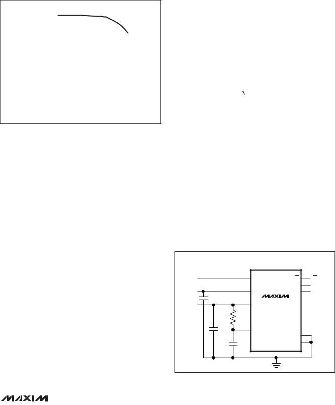
Figure 13. Effective Bits vs. Input Frequency
time between the falling edge of the sampling clock and the instant when the actual sample is taken.
Signal-to-Noise Ratio
For a waveform perfectly reconstructed from digital samples, signal-to-noise ratio (SNR) is the ratio of the full-scale analog input (RMS value) to the RMS quantization error (residual error). The ideal, theoretical minimum analog-to-digital noise is caused by quantization noise error only and results directly from the ADCs resolution (N bits):
SNR = (6.02 x N + 1.76)dB
In reality, there are other noise sources besides quantization noise: thermal noise, reference noise, clock jitter, etc. SNR is computed by taking the ratio of the RMS signal to the RMS noise, which includes all spectral components minus the fundamental, the first five harmonics, and the DC offset.
Signal-to-Noise Plus Distortion
Signal-to-noise plus distortion (SINAD) is the ratio of the fundamental input frequency’s RMS amplitude to the RMS equivalent of all the other ADC output signals.
|
|
SignalRMS |
|
|
SINAD(dB) = 20 |
log |
|
|
|
(Noise + Distortion) |
|
|||
|
|
|
|
|
|
|
|
RMS |
|
Effective Number of Bits
Effective number of bits (ENOB) indicate the global accuracy of an ADC at a specific input frequency and sampling rate. An ideal ADC error consists of quantization noise only. With an input range equal to the full-
scale range of the ADC, calculate the effective number |
MAX1062 |
|||||
sum of the first five harmonics of the input signal to the |
||||||
of bits as follows: |
|
|
|
|
|
|
ENOB = (SINAD – 1.76) / 6.02 |
|
|
||||
Figure 13 shows the effective number of bits as a func- |
|
|||||
tion of the MAX1062’s input frequency. |
|
|
|
|||
Total Harmonic Distortion |
|
|||||
Total harmonic distortion (THD) is the ratio of the RMS |
|
|||||
fundamental itself. This is expressed as: |
|
|
|
|||
|
V 2 |
+ V |
2 + V 2 |
+ V 2 |
|
|
|
2 |
3 |
4 |
5 |
|
|
THD = 20 log |
|
|
|
|
|
|
|
|
V1 |
|
|
||
|
|
|
|
|
|
|
|
|
|
|
|
|
|
where V1 is the fundamental amplitude and V2 through V5 are the 2ndthrough 5th-order harmonics.
Spurious-Free Dynamic Range
Spurious-free dynamic range (SFDR) is the ratio of the RMS amplitude of the fundamental (maximum signal component) to the RMS value of the next largest frequency component.
Supplies, Layout, Grounding and Bypassing
Use PC boards with separate analog and digital ground planes. Do not use wire-wrap boards. Connect the two ground planes together at the MAX1062 (pin 3). Isolate the digital supply from the analog with a lowvalue resistor (10Ω) or ferrite bead when the analog and digital supplies come from the same source (Figure 14).
AIN |
AIN |
CS |
CS |
VREF |
|
SCLK |
SCLK |
REF |
DOUT |
DOUT |
|
4.7µF |
|
MAX1062 |
|
+5V |
AVDD |
|
|
|
|
||
|
10Ω |
|
|
0.1µF |
DVDD |
AGND |
|
|
|
|
|
|
0.1µF |
DGND |
|
|
|
|
|
|
|
GND |
|
Figure 14. Powering AVDD and DVDD from a Single Supply
______________________________________________________________________________________ 15
14-Bit, +5V, 200ksps ADC with 10µA Shutdown
MAX1062
Constraints on sequencing the power supplies and inputs are as follows:
•Apply AGND before DGND.
•Apply AIN and REF after AVDD and AGND are present.
•DVDD is independent of the supply sequencing.
Ensure that digital return currents do not pass through the analog ground and that return-current paths are low impedance. A 5mA current flowing through a PC board ground trace impedance of only 0.05Ω creates an error voltage of about 250µV, 1LSB error with a 4V full-scale system.
The board layout should ensure that digital and analog signal lines are kept separate. Do not run analog and digital (especially the SCLK and DOUT) lines parallel to one another. If one must cross another, do so at right angles.
The ADCs high-speed comparator is sensitive to highfrequency noise on the AVDD power supply. Bypass an excessively noisy supply to the analog ground plane with a 0.1µF capacitor in parallel with a 1µF to 10µF low-ESR capacitor. Keep capacitor leads short for best supply-noise rejection.
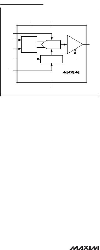
Functional Diagram
AVDD |
DVDD |
|
|
|
REF |
|
|
|
|
AIN |
14-BIT SAR |
OUTPUT |
|
|
TRACK AND |
DOUT |
|||
HOLD |
ADC |
BUFFER |
||
|
||||
AGND |
|
|
|
|
SCLK |
CONTROL |
|
|
|
CS |
|
|
|
|
|
|
MAX1062 |
|
|
|
DGND |
|
|
16 ______________________________________________________________________________________

14-Bit, +5V, 200ksps ADC with 10µA Shutdown
Chip Information
TRANSISTOR COUNT: 12,100
PROCESS: BiCMOS
Package Information
For the latest package outline information and land patterns, go to www.maxim-ic.com/packages. Note that a "+", "#", or "-" in the package code indicates RoHS status only. Package drawings may show a different suffix character, but the drawing pertains to the package regardless of RoHS status.
PACKAGE TYPE |
PACKAGE CODE |
DOCUMENT NO. |
|
|
|
10 µMAX |
U10-2 |
21-0061 |
|
|
|
MAX1062
______________________________________________________________________________________ 17

14-Bit, +5V, 200ksps ADC with 10µA Shutdown
MAX1062
|
|
|
|
Revision History |
|
|
|
|
|
|
|
REVISION |
REVISION |
|
DESCRIPTION |
|
PAGES |
NUMBER |
DATE |
|
|
CHANGED |
|
|
|
|
|||
|
|
|
|
|
|
0 |
10/01 |
Initial release |
|
|
— |
1 |
5/09 |
Updated some specifications |
|
|
1, 3 |
|
|
|
|
|
|
Maxim cannot assume responsibility for use of any circuitry other than circuitry entirely embodied in a Maxim product. No circuit patent licenses are implied. Maxim reserves the right to change the circuitry and specifications without notice at any time.
18 ____________________Maxim Integrated Products, 120 San Gabriel Drive, Sunnyvale, CA 94086 408-737-7600
© 2009 Maxim Integrated Products |
Maxim is a registered trademark of Maxim Integrated Products, Inc. |