

бакМИТ_КП2015 / Компоненты по вариантам / АЦП / MAX1157
.pdf19-2653; Rev 1; 1/03
14-Bit, 135ksps, Single-Supply ADCs with Bipolar Analog Input Range
General Description
The MAX1157/MAX1159/MAX1175 14-bit, low-power, successive-approximation analog-to-digital converters (ADCs) feature automatic power-down, a factory-trimmed internal clock, and a 14-bit wide parallel interface. The devices operate from a single +4.75V to +5.25V analog supply and feature a separate digital supply input for direct interface with +2.7V to +5.25V digital logic.
The MAX1157 accepts an analog input voltage range from 0 to +10V while the MAX1159 accepts a bipolar analog input voltage range of ±10V. The MAX1175 accepts a bipolar analog input voltage range of ±5V. All devices consume only 23mW at a sampling rate of 135ksps when using an external reference and 29mW when using the internal +4.096V reference. AutoShutdown™ reduces supply current to 0.4mA at 10ksps. The MAX1157/MAX1159/MAX1175 are ideal for high-performance, battery-powered data-acquisition applications. Excellent AC performance (THD = -100dB) and DC accuracy (±1LSB INL) make the MAX1157/ MAX1159/MAX1175 ideal for industrial process control, instrumentation, and medical applications.
The MAX1157/MAX1159/MAX1175 are available in a 28-pin TSSOP package and are fully specified over the -40°C to +85°C extended temperature range and the 0°C to +70°C commercial temperature range.
Applications
Temperature Sensing and Monitoring
Industrial Process Control
I/O Modules
Data-Acquisition Systems
Precision Instrumentation
AutoShutdown is a trademark of Maxim Integrated Products, Inc.
Features
♦Analog Input Voltage Range ±10V, ±5V, or 0 to 10V
♦14-Bit Wide Parallel Interface
♦Single +4.75V to +5.25V Analog Supply Voltage
♦Interfaces with +2.7V to +5.25V Digital Logic
♦±1LSB INL (max)
♦±1LSB DNL (max)
♦Low Supply Current (MAX1159)
5.3mA (External Reference) 6.2mA (Internal Reference) 5µA AutoShutdown Mode
♦ Small Footprint
28-Pin TSSOP Package
Pin Configuration
TOP VIEW
|
D6 |
1 |
|
|
|
|
28 |
D5 |
||||||
|
|
|
|
|
|
|
|
|
|
|
|
|
|
|
|
D7 |
2 |
|
|
|
|
27 |
D4 |
||||||
|
|
|
|
|
|
|
|
|
|
|
|
|
|
|
|
D8 |
3 |
|
|
|
|
26 |
D3 |
||||||
|
|
|
|
|
|
|
|
|
|
|
|
|
|
|
|
D9 |
4 |
|
|
|
|
25 |
D2 |
||||||
|
|
|
|
|
|
|
|
|
|
|
|
|
|
|
|
D10 |
5 |
|
|
|
|
24 |
D1 |
||||||
MAX1157 |
||||||||||||||
|
|
|
|
|
|
|
|
|
|
|||||
|
D11 |
6 |
MAX1159 |
23 |
D0 |
|||||||||
|
|
|
|
|
|
|
|
|
|
|||||
|
|
|
|
|
|
MAX1175 |
|
|
|
|
||||
|
D12 |
7 |
22 |
N.C. |
||||||||||
|
|
|
|
|
||||||||||
|
|
|
|
|
|
|
|
|
|
|
|
|
|
|
|
D13 |
8 |
|
|
|
|
21 |
N.C. |
||||||
|
|
|
|
|
|
|
|
|
|
|
|
|
|
|
|
R/C |
|
9 |
|
|
|
|
20 |
DVDD |
|||||
|
|
|
|
|
|
|
|
|
|
|
|
|
|
|
|
EOC |
|
10 |
|
|
|
|
19 |
DGND |
|||||
|
|
|
|
|
|
|
|
|
|
|
|
|
|
|
AVDD |
11 |
|
|
|
|
18 |
|
CS |
|
|||||
|
|
|
|
|
|
|
|
|
|
|
|
|
|
|
AGND |
12 |
|
|
|
|
17 |
RESET |
|||||||
|
|
|
|
|
|
|
|
|
|
|
|
|
|
|
|
AIN |
13 |
|
|
|
|
16 |
REF |
||||||
|
|
|
|
|
|
|
|
|
|
|
|
|
|
|
AGND |
14 |
|
|
|
|
15 |
REFADJ |
|||||||
TSSOP
Ordering Information
PART |
TEMP RANGE |
PIN-PACKAGE |
INPUT VOLTAGE |
INL (LSB) |
|
RANGE |
|||||
|
|
|
|
||
|
|
|
|
|
|
MAX1157ACUI |
0°C to +70°C |
28 TSSOP |
0 to +10V |
±1 |
|
|
|
|
|
|
|
MAX1157BCUI |
0°C to +70°C |
28 TSSOP |
0 to +10V |
±2 |
Ordering Information continued at end of data sheet.
________________________________________________________________ Maxim Integrated Products 1
MAX1157/MAX1159/MAX1175
For pricing, delivery, and ordering information, please contact Maxim/Dallas Direct! at 1-888-629-4642, or visit Maxim’s website at www.maxim-ic.com.

MAX1157/MAX1159/MAX1175
14-Bit, 135ksps, Single-Supply ADCs with Bipolar Analog Input Range
ABSOLUTE MAXIMUM RATINGS
AVDD to AGND ......................................................... |
|
- 0.3V to +6V |
DVDD to DGND......................................................... |
|
- 0.3V to +6V |
AGND to DGND..................................................... |
|
- 0.3V to +0.3V |
AIN to AGND ..................................................... |
|
- 16.5V to +16.5V |
REF, REFADJ to AGND............................ |
-0.3V to (AVDD + 0.3V) |
|
CS, R/C, RESET to DGND ........................................ |
|
- 0.3V to +6V |
D_, EOC to DGND ................................... |
-0.3V to (DVDD + 0.3V) |
|
Maximum Continuous Current Into Any Pin |
........................50mA |
|
Continuous Power Dissipation (TA = +70°C)
28-Pin TSSOP (derate 12.8mW/°C above +70°C) .....1026mW
Operating Temperature Range |
|
MAX11_ _ _CUI ................................................... |
0°C to +70°C |
MAX11_ _ _EUI ................................................ |
-40°C to +85°C |
Storage Temperature Range ............................. |
-65°C to +150°C |
Junction Temperature ...................................................... |
+150°C |
Lead Temperature (soldering, 10s) ................................. |
+300°C |
Stresses beyond those listed under “Absolute Maximum Ratings” may cause permanent damage to the device. These are stress ratings only, and functional operation of the device at these or any other conditions beyond those indicated in the operational sections of the specifications is not implied. Exposure to absolute maximum rating conditions for extended periods may affect device reliability.
ELECTRICAL CHARACTERISTICS
(AVDD = DVDD = +5V ±5%, external reference = +4.096V, CREF = 10µF, CREFADJ = 0.1µF, VREFADJ = AVDD, TA = TMIN to TMAX, unless otherwise noted. Typical values are at TA = +25°C.)
PARAMETER |
SYMBOL |
CONDITIONS |
MIN |
TYP |
MAX |
UNITS |
|
|
|
|
|
|
|
DC ACCURACY |
|
|
|
|
|
|
|
|
|
|
|
|
|
Resolution |
RES |
|
14 |
|
|
Bits |
|
|
|
|
|
|
|
Differential Nonlinearity |
DNL |
No missing codes over temperature |
-1 |
|
+1 |
LSB |
Integral Nonlinearity |
INL |
MAX11_ _A |
-1 |
|
+1 |
LSB |
|
|
|
|
|||
MAX11_ _B |
-2 |
|
+2 |
|||
|
|
|
|
|||
|
|
|
|
|
|
|
Transition Noise |
|
RMS noise, external reference |
|
0.32 |
|
LSBRMS |
|
Internal reference |
|
0.34 |
|
||
|
|
|
|
|
||
|
|
|
|
|
|
|
Offset Error |
|
MAX1159 |
-10 |
0 |
+10 |
mV |
|
|
|
|
|
||
|
MAX1157/MAX1175 |
-10 |
|
+10 |
||
|
|
|
|
|||
Gain Error |
|
|
|
0 |
±0.2 |
%FSR |
|
|
|
|
|
|
|
Offset Drift |
|
|
|
16 |
|
µV/°C |
|
|
|
|
|
|
|
Gain Drift |
|
|
|
±1 |
|
ppm/°C |
AC ACCURACY (fIN = 1kHz, VAIN = full range, 135ksps)
Signal-to-Noise Plus Distortion |
SINAD |
|
|
81 |
85 |
|
dB |
|
|
|
|
|
|
|
|
Signal-to-Noise Ratio |
SNR |
|
|
82 |
85 |
|
dB |
|
|
|
|
|
|
|
|
Total Harmonic Distortion |
THD |
|
|
|
-100 |
-86 |
dB |
Spurious-Free Dynamic Range |
SFDR |
|
|
87 |
103 |
|
dB |
|
|
|
|
|
|
|
|
ANALOG INPUT |
|
|
|
|
|
|
|
|
|
|
|
|
|
|
|
|
|
MAX1157 |
|
0 |
|
+10 |
|
Input Range |
VAIN |
MAX1159 |
|
-10 |
|
+10 |
V |
|
|
MAX1175 |
|
-5 |
|
+5 |
|
|
|
|
|
|
|
|
|
|
|
MAX1157/MAX1175 |
Normal operation |
5.3 |
6.9 |
9.2 |
|
|
|
MAX1175 |
Shutdown mode |
3 |
|
|
|
Input Resistance |
RAIN |
MAX1157 |
Shutdown mode |
5.3 |
|
|
kΩ |
|
|
MAX1159 |
Normal operation |
7.8 |
10 |
13.0 |
|
|
|
Shutdown mode |
6 |
|
|
|
|
|
|
|
|
|
|
||
|
|
|
|
|
|
|
|
2 _______________________________________________________________________________________ 


14-Bit, 135ksps, Single-Supply ADCs with Bipolar Analog Input Range
ELECTRICAL CHARACTERISTICS (continued)
(AVDD = DVDD = +5V ±5%, external reference = +4.096V, CREF = 10µF, CREFADJ = 0.1µF, VREFADJ = AVDD, TA = TMIN to TMAX, unless otherwise noted. Typical values are at TA = +25°C.)
PARAMETER |
SYMBOL |
CONDITIONS |
MIN |
TYP |
MAX |
UNITS |
|
|
|
|
|
|
|
|
|
|
|
MAX1157, |
Normal/shutdown |
-0.1 |
|
+2.0 |
|
|
|
0 ≤ VAIN ≤ +10V |
mode |
|
|
||
|
|
|
|
|
|
||
Input Current |
IAIN |
MAX1159, |
Normal operation |
-1.8 |
|
+1.2 |
mA |
-10V ≤ VAIN ≤ +10V |
Shutdown mode |
-1.8 |
|
+1.8 |
|||
|
|
|
|
||||
|
|
MAX1175, |
Normal operation |
-1.8 |
|
+0.4 |
|
|
|
-5V ≤ VAIN ≤ +5V |
Shutdown mode |
-1.8 |
|
+1.8 |
|
|
|
MAX1159, VAIN = +10V, shutdown mode to |
|
0.5 |
0.7 |
|
|
|
|
operating mode |
|
|
|
||
Input Current Step at Power-Up |
IPU |
|
|
|
|
mA |
|
|
|
|
|
|
|||
MAX1175, VAIN = +5V, shutdown mode to |
|
1 |
1.4 |
||||
|
|
|
|
||||
|
|
operating mode |
|
|
|
||
|
|
|
|
|
|
|
|
|
|
|
|
|
|
|
|
Input Capacitance |
CIN |
|
|
|
10 |
|
pF |
INTERNAL REFERENCE |
|
|
|
|
|
|
|
|
|
|
|
|
|
|
|
REF Output Voltage |
VREF |
|
|
4.056 |
4.096 |
4.136 |
V |
REF Output Tempco |
|
|
|
|
±35 |
|
ppm/°C |
|
|
|
|
|
|
|
|
REF Short-Circuit Current |
IREF-SC |
|
|
|
±10 |
|
mA |
EXTERNAL REFERENCE |
|
|
|
|
|
|
|
REF and REFADJ Input Voltage |
|
|
|
3.8 |
|
4.2 |
V |
Range |
|
|
|
|
|||
|
|
|
|
|
|
|
|
|
|
|
|
|
|
|
|
REFADJ Buffer Disable Threshold |
|
|
|
AVDD - |
|
AVDD - |
V |
|
|
|
0.4 |
|
0.1 |
||
|
|
|
|
|
|
||
|
|
|
|
|
|
|
|
REF Input Current |
IREF |
Normal mode, fSAMPLE = 135ksps |
|
60 |
100 |
µA |
|
Shutdown mode (Note 1) |
|
±0.1 |
±10 |
||||
|
|
|
|
||||
REFADJ Input Current |
IREFADJ |
REFADJ = AVDD |
|
|
16 |
|
µA |
DIGITAL INPUTS/OUTPUTS |
|
|
|
|
|
|
|
|
|
|
|
|
|
|
|
Output High Voltage |
VOH |
ISOURCE = 0.5mA, DVDD = +2.7V to +5.25V, |
DVDD - |
|
|
V |
|
AVDD = +5.25V |
|
0.4 |
|
|
|||
|
|
|
|
|
|
||
Output Low Voltage |
VOL |
ISINK = 1.6mA, DVDD = +2.7V to +5.25V, |
|
|
0.4 |
V |
|
AVDD = +5.25V |
|
|
|
||||
|
|
|
|
|
|
|
|
Input High Voltage |
VIH |
|
|
0.7 × |
|
|
V |
|
|
DVDD |
|
|
|||
|
|
|
|
|
|
|
|
|
|
|
|
|
|
|
|
Input Low Voltage |
VIL |
|
|
|
|
0.3 × |
V |
|
|
|
|
DVDD |
|||
|
|
|
|
|
|
|
|
Input Leakage Current |
|
Digital input = DVDD or 0V |
-1 |
|
+1 |
µA |
|
Input Hysteresis |
VHYST |
|
|
|
0.2 |
|
V |
Input Capacitance |
CIN |
|
|
|
15 |
|
pF |
Three-State Output Leakage |
IOZ |
|
|
|
|
±10 |
µA |
Three-State Output Capacitance |
COZ |
|
|
|
15 |
|
pF |
|
|
|
|
|
|
|
|
MAX1157/MAX1159/MAX1175
_______________________________________________________________________________________ 3

MAX1157/MAX1159/MAX1175
14-Bit, 135ksps, Single-Supply ADCs with Bipolar Analog Input Range
ELECTRICAL CHARACTERISTICS (continued)
(AVDD = DVDD = +5V ±5%, external reference = +4.096V, CREF = 10µF, CREFADJ = 0.1µF, VREFADJ = AVDD, TA = TMIN to TMAX, unless otherwise noted. Typical values are at TA = +25°C.)
PARAMETER |
SYMBOL |
CONDITIONS |
MIN |
TYP |
MAX |
UNITS |
|
POWER SUPPLIES |
|
|
|
|
|
|
|
|
|
|
|
|
|
|
|
Analog Supply Voltage |
AVDD |
|
|
4.75 |
|
5.25 |
V |
Digital Supply Voltage |
DVDD |
|
|
2.70 |
|
5.25 |
V |
|
|
External reference, |
MAX1157 |
|
|
2.9 |
|
Analog Supply Current |
IAVDD |
135ksps |
MAX1159/MAX1175 |
|
4.0 |
5.3 |
mA |
|
|
|
|
|
|||
Internal reference, |
MAX1157 |
|
|
3.8 |
|||
|
|
|
|
|
|||
|
|
135ksps |
MAX1159/MAX1175 |
|
5.2 |
6.2 |
|
|
|
Shutdown mode (Note 1), digital input = |
|
0.5 |
5 |
µA |
|
Shutdown Supply Current |
ISHDN |
DVDD or 0V |
|
|
|||
|
|
|
|
|
|||
|
|
Standby mode |
|
|
3.7 |
|
mA |
|
|
|
|
|
|
|
|
Digital Supply Current |
IDVDD |
|
|
|
|
0.75 |
mA |
Power-Supply Rejection |
|
AVDD = DVDD = +4.75V to +5.25V |
|
1 |
|
LSB |
|
|
|
|
|
|
|
|
|
TIMING CHARACTERISTICS (Figures 1 and 2)
(AVDD = +4.75V to +5.25V, DVDD = +2.7V to AVDD, external reference = +4.096V, CREF = 10µF, CREFADJ = 0.1µF, VREFADJ = AVDD, CLOAD = 20pF, TA = TMIN to TMAX.)
PARAMETER |
SYMBOL |
CONDITIONS |
MIN |
TYP |
MAX |
UNITS |
|
Maximum Sampling Rate |
fSAMPLE-MAX |
|
|
|
|
135 |
ksps |
Acquisition Time |
tACQ |
|
|
2 |
|
|
µs |
Conversion Time |
tCONV |
|
|
|
|
4.7 |
µs |
CS Pulse Width High |
tCSH |
(Note 2) |
40 |
|
|
ns |
|
CS Pulse Width Low |
tCSL |
(Note 2) |
DVDD = +4.75V to +5.25V |
40 |
|
|
ns |
DVDD = +2.7V to +5.25V |
60 |
|
|
||||
|
|
|
|
|
|
||
R/C to CS Fall Setup Time |
tDS |
|
|
0 |
|
|
ns |
R/C to CS Fall Hold Time |
tDH |
DVDD = +4.75V to +5.25V |
40 |
|
|
ns |
|
DVDD = +2.7V to +5.25V |
60 |
|
|
||||
|
|
|
|
|
|||
CS to Output Data Valid |
tDO |
DVDD = +4.75V to +5.25V |
|
|
40 |
ns |
|
DVDD = +2.7V to +5.25V |
|
|
80 |
||||
|
|
|
|
|
|||
EOC Fall to CS Fall |
tDV |
|
|
0 |
|
|
ns |
CS Rise to EOC Rise |
tEOC |
DVDD = +4.75V to +5.25V |
|
|
40 |
ns |
|
DVDD = +2.7V to +5.25V |
|
|
80 |
||||
|
|
|
|
|
|||
Bus Relinquish Time |
tBR |
DVDD = +4.75V to +5.25V |
|
|
40 |
ns |
|
DVDD = +2.7V to +5.25V |
|
|
80 |
||||
|
|
|
|
|
|||
Note 1: Maximum specification is limited by automated test equipment.
Note 2: To ensure best performance, finish reading the data and wait tBR before starting a new acquisition.
4 _______________________________________________________________________________________
14-Bit, 135ksps, Single-Supply ADCs with Bipolar Analog Input Range
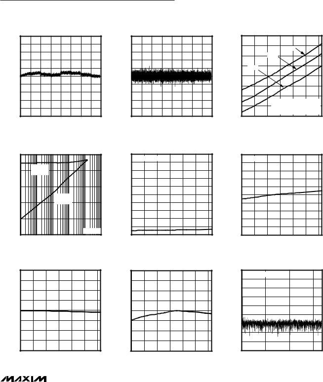
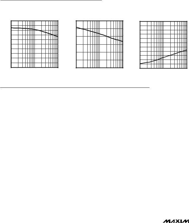
Typical Operating Characteristics
(AVDD = DVDD = +5V, external reference = +4.096V, CREF = 10µF, CREFADJ = 0.1µF, VREFADJ = AVDD, CLOAD = 20pF, TA = TMIN to TMAX, unless otherwise noted. Typical values are at TA = +25°C.) (Typical Application Circuit)
INL (LSB)
2.5
2.0
1.5
1.0
0.5
0 -0.5 -1.0 -1.5 -2.0 -2.5
INL vs. CODE
MAX1157 toc01
0 |
4096 |
8192 |
12288 |
16384 |
CODE
DNL (LSB)
1.0
0.8
0.6
0.4
0.2
0 -0.2 -0.4 -0.6 -0.8
-1.0
0
DNL vs. CODE |
SUPPLY CURRENT (AVDD + DVDD) |
vs. TEMPERATURE |
|
|
|
toc02 |
|
4.80 |
|
|
|
|
|
toc03 |
|
|
|
|
|
|
|
|
|
|
||
|
|
|
MAX1157 |
|
4.75 |
|
|
|
5.25V |
|
MAX1157 |
|
|
|
|
|
|
|
|
|
|||
|
|
|
|
(mA) |
4.70 |
|
|
5.0V |
|
|
|
|
|
|
|
|
|
|
|
|
|
|
|
|
|
|
|
CURRENT |
4.65 |
4.75V |
|
|
|
|
|
|
|
|
|
|
|
|
|
|
|
||
|
|
|
|
4.60 |
|
|
|
|
|
|
|
|
|
|
|
|
|
|
|
|
|
|
|
|
|
|
|
SUPPLY |
4.55 |
|
|
|
|
|
|
|
|
|
|
4.50 |
|
|
|
|
|
|
|
|
|
|
|
|
|
|
|
fSAMPLE = 135ksps |
|||
|
|
|
|
|
4.45 |
|
|
|
|||
|
|
|
|
|
|
|
SHUTDOWN MODE BETWEEN |
||||
|
|
|
|
|
4.40 |
|
|
|
|
CONVERSIONS |
|
|
|
|
|
|
|
|
|
|
|
|
|
4096 |
8192 |
12288 |
16384 |
|
-40 |
-20 |
0 |
20 |
40 |
60 |
80 |
CODE |
TEMPERATURE (°C) |
SUPPLY CURRENT (AVDD + DVDD) |
SHUTDOWN CURRENT (AVDD + DVDD) |
|
vs. SAMPLE RATE |
vs. TEMPERATURE |
OFFSET ERROR vs. TEMPERATURE |
10 |
|
|
|
|
toc04 |
|
5.0 |
|
|
|
|
|
|
toc05 |
|
10 |
|
|
|
|
|
toc06 |
|
|
|
|
|
|
NO CONVERSIONS |
|
|
|
|
|
MAX1159 |
|
|
|
|
||||||
|
STANDBY |
|
|
|
MAX1157 |
(mA) |
4.5 |
|
|
|
|
|
|
MAX1157 |
|
8 |
|
|
|
|
|
MAX1157 |
1 |
|
|
|
4.0 |
|
|
|
|
|
|
|
6 |
|
|
|
|
|
|||||
|
|
|
|
|
|
|
|
|
|
|
|
|
|
|
|
|
|
|
||||
MODE |
|
|
|
|
CURRENTSUPPLYSHUTDOWN |
|
|
|
|
|
|
|
|
|
|
|
|
|
|
|||
(mA)CURRENTSUPPLY |
|
|
|
|
|
|
|
|
|
|
|
|
(mV)ERROROFFSET |
|
|
|
|
|
|
|
||
|
|
|
|
|
3.5 |
|
|
|
|
|
|
|
4 |
|
|
|
|
|
|
|||
|
|
|
|
|
|
|
|
|
|
|
|
|
|
|
|
|
|
|
|
|
||
0.1 |
|
|
|
|
|
|
3.0 |
|
|
|
|
|
|
|
|
2 |
|
|
|
|
|
|
|
|
SHUTDOWN |
|
|
|
2.5 |
|
|
|
|
|
|
|
|
0 |
|
|
|
|
|
|
|
0.01 |
|
|
MODE |
|
|
|
2.0 |
|
|
|
|
|
|
|
|
-2 |
|
|
|
|
|
|
|
|
|
|
|
|
|
1.5 |
|
|
|
|
|
|
|
|
-4 |
|
|
|
|
|
|
0.001 |
|
|
|
|
|
|
1.0 |
|
|
|
|
|
|
|
|
-6 |
|
|
|
|
|
|
|
|
|
|
VAIN = 0V |
|
0.5 |
|
|
|
|
|
|
|
|
-8 |
|
|
|
|
|
|
|
0.0001 |
|
|
|
|
0 |
|
|
|
|
|
|
|
|
-10 |
|
|
|
|
|
|
||
|
|
|
|
|
|
-20 |
0 |
20 |
40 |
60 |
|
|
|
|
|
|
|
|
|
|||
0.01 |
0.1 |
1 |
10 |
100 |
1000 |
|
-40 |
80 |
|
|
-40 |
-20 |
0 |
20 |
40 |
60 |
80 |
|||||
|
SAMPLE RATE (ksps) |
|
|
|
|
|
TEMPERATURE (°C) |
|
|
|
|
|
|
TEMPERATURE (°C) |
|
|
||||||
GAIN ERROR vs. TEMPERATURE |
INTERNAL REFERENCE |
FFT AT 1kHz |
vs. TEMPERATURE |
|
0.20 |
|
|
|
|
|
toc07 |
|
4.136 |
|
|
|
|
|
toc08 |
|
0 |
fSAMPLE = 135ksps |
|
toc09 |
|
|
|
|
|
|
|
|
|
|
|
|
|
|
|
|
|
||||
|
0.15 |
|
|
|
|
|
MAX1157 |
|
4.126 |
|
|
|
|
|
MAX1157 |
|
-20 |
|
|
MAX1157 |
|
|
|
|
|
|
|
|
|
|
|
|
|
|
|
|
|
|
|||
|
0.10 |
|
|
|
|
|
|
REFERENCEINTERNAL(V) |
4.116 |
|
|
|
|
|
|
|
-40 |
|
|
|
(%FSR)ERRORGAIN |
|
|
|
|
|
|
|
|
|
|
|
|
(dB)MAGNITUDE |
|
|
|
|
|||
0.05 |
|
|
|
|
|
|
4.106 |
|
|
|
|
|
|
-60 |
|
|
|
|||
|
|
|
|
|
|
|
|
|
|
|
|
|
|
|
|
|
|
|||
|
|
|
|
|
|
|
|
|
|
|
|
|
|
|
-80 |
|
|
|
||
|
0 |
|
|
|
|
|
|
|
4.096 |
|
|
|
|
|
|
|
|
|
|
|
|
|
|
|
|
|
|
|
|
|
|
|
|
|
|
-100 |
|
|
|
||
|
|
|
|
|
|
|
|
|
|
|
|
|
|
|
|
|
|
|
|
|
|
-0.05 |
|
|
|
|
|
|
|
4.086 |
|
|
|
|
|
|
|
-120 |
|
|
|
|
|
|
|
|
|
|
|
|
|
|
|
|
|
|
|
|
|
|
|
|
|
-0.10 |
|
|
|
|
|
|
|
4.076 |
|
|
|
|
|
|
|
-140 |
|
|
|
|
|
|
|
|
|
|
|
|
|
|
|
|
|
|
|
|
|
|
|
|
|
-0.15 |
|
|
|
|
|
|
|
4.066 |
|
|
|
|
|
|
|
-160 |
|
|
|
|
-0.20 |
|
|
|
|
|
|
|
4.056 |
|
|
|
|
|
|
|
-180 |
20 |
40 |
|
|
-40 |
-20 |
0 |
20 |
40 |
60 |
80 |
|
-40 |
-20 |
0 |
20 |
40 |
60 |
80 |
|
0 |
60 |
||
|
|
|
TEMPERATURE (°C) |
|
|
|
|
|
TEMPERATURE (°C) |
|
|
|
|
FREQUENCY (kHz) |
|
|||||
MAX1157/MAX1159/MAX1175
_______________________________________________________________________________________ 5
MAX1157/MAX1159/MAX1175
14-Bit, 135ksps, Single-Supply ADCs with Bipolar Analog Input Range
Typical Operating Characteristics
(AVDD = DVDD = +5V, external reference = +4.096V, CREF = 10µF, CREFADJ = 0.1µF, VREFADJ = AVDD, CLOAD = 20pF, TA = TMIN to TMAX, unless otherwise noted. Typical values are at TA = +25°C.) (Typical Application Circuit)
SINAD vs. FREQUENCY
|
100 |
|
toc10 |
|
120 |
|
90 |
|
|
|
|
|
|
MAX1157 |
|
|
|
|
80 |
|
|
100 |
|
|
|
|
|
|
|
|
70 |
|
|
|
80 |
(dB) |
60 |
|
|
|
|
|
|
(dB) |
|
||
|
|
|
|
||
SINAD |
50 |
|
|
SFDR |
60 |
40 |
|
|
|
||
|
|
|
|
|
|
|
30 |
|
|
|
40 |
|
|
|
|
|
|
|
20 |
|
|
|
20 |
|
10 |
|
|
|
|
|
|
|
|
|
|
|
0 |
10 |
|
|
0 |
|
1 |
100 |
|
|
FREQUENCY (kHz)
SPURIOUS-FREE DYNAMIC RANGE vs. FREQUENCY
|
|
toc11 |
0 |
|
|
-10 |
|
|
|
MAX1157 |
|
|
|
-20 |
|
|
|
|
|
|
|
|
-30 |
|
|
(dB) |
-40 |
|
|
-50 |
|
|
|
THD |
-60 |
|
|
|
-70 |
|
|
|
-80 |
|
|
|
-90 |
|
|
|
-100 |
1 |
10 |
100 |
-110 |
|
FREQUENCY (kHz)
TOTAL HARMONIC DISTORTION vs. FREQUENCY
|
|
MAX1157 toc12 |
1 |
10 |
100 |
FREQUENCY (kHz)
Pin Description
PIN |
NAME |
FUNCTION |
|
|
|
|
|
1 |
D6 |
Three-State Digital Data Output |
|
|
|
|
|
2 |
D7 |
Three-State Digital Data Output |
|
|
|
|
|
3 |
D8 |
Three-State Digital Data Output |
|
|
|
|
|
4 |
D9 |
Three-State Digital Data Output |
|
|
|
|
|
5 |
D10 |
Three-State Digital Data Output |
|
|
|
|
|
6 |
D11 |
Three-State Digital Data Output |
|
|
|
|
|
7 |
D12 |
Three-State Digital Data Output |
|
|
|
|
|
8 |
D13 |
Three-State Digital Data Output (MSB) |
|
|
|
|
|
|
|
Read/Convert Input. Power up and place the MAX1157/MAX1159/MAX1175 in acquisition mode by |
|
|
|
holding R/C low during the first falling edge of CS. During the second falling edge of CS, the level on |
|
9 |
R/C |
R/C determines whether the reference and reference buffer power down or remain on after |
|
conversion. Set R/C high during the second falling edge of CS to power down the reference and |
|||
|
|
||
|
|
buffer, or set R/C low to leave the reference and buffer powered up. Set R/C high during the third |
|
|
|
falling edge of CS to put valid data on the bus. |
|
|
|
|
|
10 |
EOC |
End of Conversion. EOC drives low when conversion is complete. |
|
|
|
|
|
11 |
AVDD |
Analog Supply Input. Bypass with a 0.1µF capacitor to AGND. |
|
12 |
AGND |
Analog Ground. Primary analog ground (star ground). |
|
|
|
|
|
13 |
AIN |
Analog Input |
|
|
|
|
|
14 |
AGND |
Analog Ground. Connect pin 14 to pin 12. |
|
|
|
|
6 _______________________________________________________________________________________
14-Bit, 135ksps, Single-Supply ADCs with Bipolar Analog Input Range
|
|
|
Pin Description (continued) |
|
|
|
|
||
PIN |
NAME |
FUNCTION |
||
|
|
|
||
15 |
REFADJ |
Reference Buffer Output. Bypass REFADJ with a 0.1µF capacitor to AGND for internal reference |
||
mode. Connect REFADJ to AVDD to select external reference mode. |
||||
|
|
|||
16 |
REF |
Reference Input/Output. Bypass REF with a 10µF capacitor to AGND. REF is the external reference |
||
input when in external reference mode. |
||||
|
|
|||
|
|
|
||
17 |
RESET |
Reset Input. Logic high resets the device. |
||
|
|
|
||
|
|
Convert Start. The first falling edge of CS powers up the device and enables acquisition when R/C |
||
18 |
CS |
is low. The second falling edge of CS starts conversion. The third falling edge of CS loads the result |
||
|
|
onto the bus when R/C is high. |
||
|
|
|
||
19 |
DGND |
Digital Ground |
||
|
|
|
||
20 |
DVDD |
Digital Supply Voltage. Bypass with a 0.1µF capacitor to DGND. |
||
21, 22 |
N.C. |
No Connection. Make no connection to these pins. |
||
|
|
|
||
23 |
D0 |
Three-State Digital Data Output (LSB) |
||
|
|
|
||
24 |
D1 |
Three-State Digital Data Output |
||
|
|
|
||
25 |
D2 |
Three-State Digital Data Output |
||
|
|
|
||
26 |
D3 |
Three-State Digital Data Output |
||
|
|
|
||
27 |
D4 |
Three-State Digital Data Output |
||
|
|
|
||
28 |
D5 |
Three-State Digital Data Output |
||
|
|
|
|
|
Detailed Description
Converter Operation
The MAX1157/MAX1159/MAX1175 use a successiveapproximation (SAR) conversion technique with an inherent track-and-hold (T/H) stage to convert an analog input into a 14-bit digital output. Parallel outputs provide a high-speed interface to microprocessors (µPs). The Functional Diagram at the end of the data sheet shows a simplified internal architecture of the MAX1157/ MAX1159/MAX1175. Figure 3 shows a typical application circuit for the MAX1157/MAX1159/MAX1175.
Analog Input
Input Scaler
The MAX1157/MAX1159/MAX1175 have an input scaler which allows conversion of true bipolar input voltages and input voltages greater than the power supply, while operating from a single +5V analog supply. The input scaler attenuates and shifts the analog input to match the input range of the internal DAC. The MAX1157 has a unipolar input voltage range of 0 to +10V. The
|
|
|
|
|
|
DVDD |
|||
|
|
|
|
|
|
|
|
|
|
D0–D13 |
|
|
|
|
D0–D13 |
1mA |
|
|
|
|
|
|
|
|
|||||
|
|
|
|
|
|
|
|||
|
|
|
|
|
|
|
|
||
|
|
|
|
|
|
|
|
||
|
|
|
|
|
|||||
1mA |
CLOAD = 20pF |
|
|
|
CLOAD = 20pF |
||||
|
|
|
|
|
DGND |
||||
|
|
|
DGND |
|
|
|
|
|
|
|
A) HIGH-Z TO VOH, |
B) HIGH-Z TO VOL, |
|||||||
|
VOL TO VOH, AND |
VOH TO VOL, AND |
|||||||
|
VOH TO HIGH-Z |
VOL TO HIGH-Z |
|||||||
Figure 1. Load Circuits
MAX1175 input voltage range is ±5V while the MAX1159 input voltage range is ±10V. Figure 4 shows the equivalent input circuit of the MAX1157/ MAX1159/MAX1175. This circuit limits the current going into or out of AIN to less than 1.8mA.
MAX1157/MAX1159/MAX1175
_______________________________________________________________________________________ 7
MAX1157/MAX1159/MAX1175
14-Bit, 135ksps, Single-Supply ADCs with Bipolar Analog Input Range
tCSL |
tCSH |
|
|
|
CS |
|
|
|
|
|
tACQ |
|
|
|
R/C |
REF POWER- |
|
|
|
DOWN CONTROL |
|
|
||
|
|
tEOC |
||
tDH |
tDS |
tDV |
||
|
||||
EOC |
|
|
|
|
HIGH-Z |
tCONV |
tDO |
tBR |
|
HIGH-Z |
||||
|
|
|
||
D0–D13 |
|
|
DATA VALID |
Figure 2. MAX1157/MAX1159/MAX1175 Timing Diagram
+5V ANALOG |
+5V DIGITAL |
0.1 F |
|
|
|
0.1 F |
|
|
AVDD |
|
DVDD |
P DATA |
|
|
|
BUS |
|
||
ANALOG |
AIN |
|
D0–D13 |
14-BIT |
|
|
WIDE |
|
|||
INPUT |
|
|
|
|
|
|
|
MAX1157 |
|
|
|
|
R/C |
MAX1159 |
EOC |
|
|
|
MAX1175 |
|
|
||
|
|
|
|
|
|
|
CS |
|
REF |
|
|
|
|
|
|
|
|
|
RESET |
|
REFADJ |
|
|
|
|
AGND DGND |
0.1 F |
10 F |
|
Figure 3. Typical Application Circuit for the MAX1157/MAX1159/ MAX1175
Track and Hold (T/H)
In track mode, the internal hold capacitor acquires the analog signal (see Figure 4). In hold mode, the T/H switches open and the capacitive DAC samples the analog input. During the acquisition, the analog input (AIN) charges capacitor CHOLD. The acquisition ends on the second falling edge of CS. At this instant, the T/H switches open. The retained charge on CHOLD represents a sample of the input. In hold mode, the capacitive DAC adjusts during the remainder of the conversion time to restore node T/H OUT to zero within the limits of 14-bit resolution. Force CS low to put valid data on the bus after conversion is complete.
Power-Down Modes
Select standby mode or shutdown mode with R/C during the second falling edge of CS (see Selecting Standby or Shutdown Mode section). The MAX1157/MAX1159/ MAX1175 automatically enter either standby mode (reference and buffer on), or shutdown (reference and buffer off) after each conversion depending on the status of R/C during the second falling edge of CS.
Internal Clock
The MAX1157/MAX1159/MAX1175 generate an internal conversion clock to free the microprocessor from the burden of running the SAR conversion clock. Total conversion time after entering hold mode (second falling edge of CS) to end-of-conversion (EOC) falling is 4.7µs (max).
Applications Information
Starting a Conversion
CS and R/C control acquisition and conversion in the MAX1157/MAX1159/MAX1175 (see Figure 2). The first falling edge of CS powers up the device and puts it in acquire mode if R/C is low. The convert start CS is ignored if R/C is high. The MAX1157/MAX1159/ MAX1175 need at least 6ms (CREFADJ = 0.1µF, CREF = 10µF) for the internal reference to wake up and settle before starting the conversion if powering up from shutdown. Reset the MAX1157/MAX1159/MAX1175 by toggling RESET with CS high. The next falling edge of CS begins acquisition.
Selecting Standby or Shutdown Mode
The MAX1157/MAX1159/MAX1175 have a selectable standby or low-power shutdown mode. In standby mode, the ADC’s internal reference and reference buffer do not power down between conversions, eliminating the need to wait for the reference to power up before performing the next conversion. Shutdown mode
8 _______________________________________________________________________________________
14-Bit, 135ksps, Single-Supply ADCs with Bipolar Analog Input Range
MAX1157
R2 161Ω
AIN
R3
3.4kΩ |
CHOLD |
|
|
TRACK |
|
||
30pF |
|
||
|
S1 |
T/H OUT |
|
HOLD TRACK |
|||
HOLD |
|||
|
|
S2 |
|
S1, S2 = T/H SWITCH S3 = POWER-DOWN (MAX1159/MAX1175 ONLY)
|
|
|
|
REF |
|
MAX1159/MAX1175 |
3.4kΩ |
|
|
|
|
|
|
|
|
|
|
R2 |
161Ω |
|
TRACK |
CHOLD |
|
AIN |
|
|
30pF |
|
|
|
|
|
S1 |
|
|
|
|
|
|
T/H OUT |
|
|
|
|
HOLD TRACK |
||
|
R3 |
S3 |
HOLD |
||
|
POWER- |
|
|
S2 |
|
|
|
DOWN |
|
|
|
R2 = 7.85kΩ (MAX1159)
OR 3.92kΩ (MAX1157/MAX1175)
R3 = 5.45kΩ (MAX1159)
OR 17.79kΩ (MAX1157/MAX1175)
Figure 4. Equivalent Input Circuit
ACQUISITION |
CONVERSION |
DATA |
|
OUT |
|||
|
|
CS
R/C
EOC
REF AND
BUFFER
POWER
Figure 5. Selecting Standby Mode
powers down the reference and reference buffer after completing a conversion. The reference and reference buffer require a minimum of 12ms (CREFADJ = 0.1µF, CREF = 10µF) to power up and settle from shutdown.
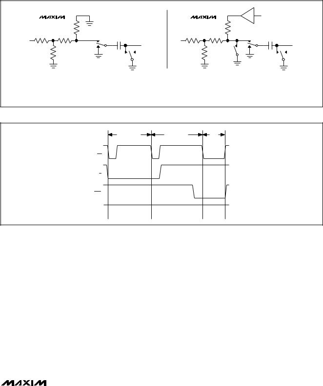
The state of R/C during the second falling edge of CS selects which power-down mode the MAX1157/ MAX1159/MAX1175 enters upon conversion completion. Holding R/C low causes the MAX1157/MAX1159/ MAX1175 to enter standby mode. The reference and buffer are left on after the conversion completes. R/C high causes the MAX1157/MAX1159/MAX1175 to enter shutdown mode and power down the reference and buffer after conversion (see Figures 5 and 6). Set the voltage at REF high during the second falling edge of CS to realize the lowest current operation.
Standby Mode
While in standby mode, the supply current is less than 3.7mA (typ). The next falling edge of CS with R/C low causes the MAX1157/MAX1159/MAX1175 to exit standby mode and begin acquisition. The reference and reference buffer remain active to allow quick turn-on time.
MAX1157/MAX1159/MAX1175
_______________________________________________________________________________________ 9
MAX1157/MAX1159/MAX1175
14-Bit, 135ksps, Single-Supply ADCs with Bipolar Analog Input Range
ACQUISITION CONVERSION
DATA
OUT
CS
R/C
EOC
REF AND
BUFFER
POWER
Figure 6. Selecting Shutdown Mode
+5V |
MAX1157 |
|
MAX1159 |
||
|
MAX1175 |
|
100kΩ |
68kΩ |
|
REFADJ |
||
|
||
|
0.1µF |
|
150kΩ |
|
Figure 7. MAX1157/MAX1159/MAX1175 Reference Adjust
Circuit
Shutdown Mode
In shutdown mode, the reference and reference buffer shut down between conversions. Shutdown mode reduces supply current to 0.5µA (typ) immediately after the conversion. The next falling edge of CS with R/C low causes the reference and buffer to wake up and enter acquisition mode. To achieve 14-bit accuracy, allow 12ms (CREFADJ = 0.1µF, CREF = 10µF) for the internal reference to wake up.
Internal and External Reference
Internal Reference
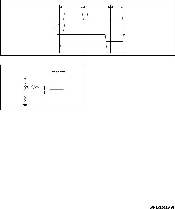
The internal reference of the MAX1157/MAX1159/ MAX1175 is internally buffered to provide +4.096V output at REF. Bypass REF to AGND and REFADJ to AGND with 10µF and 0.1µF, respectively.
Sink or source current at REFADJ to make fine adjustments to the internal reference. The input impedance of REFADJ is nominally 5kΩ. Use the circuit of Figure 7 to adjust the internal reference to ±1.5%.
External Reference
An external reference can be placed at either the input (REFADJ) or the output (REF) of the MAX1157/ MAX1159/MAX1175’s internal buffer amplifier. Using the buffered REFADJ input makes buffering the external reference unnecessary. The input impedance of REFADJ is typically 5kΩ. The internal buffer output must be bypassed at REF with a 10µF capacitor.
Connect REFADJ to AVDD to disable the internal buffer. Directly drive REF using an external 3.8V to 4.2V reference. During conversion, the external reference must be able to drive 100µA of DC load current and have an output impedance of 10Ω or less.
For optimal performance, buffer the reference through an op amp and bypass REF with a 10µF capacitor. Consider the MAX1157/MAX1159/MAX1175’s equivalent input noise (0.6LSB) when choosing a reference.
Reading the Conversion Result
EOC flags the microprocessor when a conversion is complete. The falling edge of EOC signals that the data is valid and ready to be output to the bus. D0–D13 are the parallel outputs of the MAX1157/MAX1159/ MAX1175. These three-state outputs allow for direct connection to a microcontroller I/O bus. The outputs remain high-impedance during acquisition and conversion. Data is loaded onto the bus with the third falling edge of CS with R/C high (after tDO). Bringing CS high forces the output bus back to high impedance. The MAX1157/MAX1159/MAX1175 then wait for the next falling edge of CS to start the next conversion cycle (see Figure 2).
10 ______________________________________________________________________________________