

бакМИТ_КП2015 / Компоненты по вариантам / АЦП / MAX194
.pdf19-0345; Rev 4; 12/97
KIT
EVALUATION
AVAILABLE
Description
-approximation anathat combines high consumption, and a calibration circuitry corto maintain the full rated temperature range
. The capacitive-DAC 85ksps track/hold
reference (up to +5V), bipolar (-VREF to VREF) analog and digital
coupling.
____________________________Features
♦ True 14-Bit Accuracy: 1⁄2LSB INL
82dB SINAD
♦9.4µs Conversion Time
♦10µA Shutdown Mode
♦Built-In Track/Hold
♦AC and DC Specified
♦Unipolar (0V to VREF) and Bipolar (-VREF to VREF) Input Range
♦Three-State Serial-Data Output
♦Small 16-Pin DIP, SO, and Ceramic SB Packages
♦Pin-Compatible 16-Bit Upgrade (MAX195)
|
|
|
the three-state seri- |
______________Ordering Information |
||||||||
|
|
|
be read either during |
|||||||||
|
|
|
|
or following con- |
PART |
TEMP. RANGE |
PIN-PACKAGE |
|
||||
|
|
|
the serial clock (SCLK). |
|
||||||||
|
|
|
output can be used to |
MAX194ACPE |
0°C to +70°C |
16 Plastic DIP |
|
|||||
|
|
|
connected directly to |
MAX194BCPE |
0°C to +70°C |
16 Plastic DIP |
|
|||||
|
|
|
continuous, full-speed |
MAX194ACWE |
0°C to +70°C |
16 Wide SO |
|
|||||
|
|
|
|
|
|
|||||||
|
|
|
-pin DIP, wide SO, and |
MAX194BCWE |
0°C to +70°C |
16 Wide SO |
|
|||||
|
|
|
MAX194AEPE |
-40°C to +85°C |
16 Plastic DIP |
|
||||||
|
|
|
The output data format |
|
||||||||
|
|
|
MAX194BEPE |
-40°C to +85°C |
16 Plastic DIP |
|
||||||
|
|
|
|
compatibility with |
|
|||||||
|
|
|
|
MAX194AEWE |
-40°C to +85°C |
16 Wide SO |
|
|||||
|
|
|
|
|
|
|||||||
________________________Applications |
MAX194BEWE |
-40°C to +85°C |
16 Wide SO |
|
||||||||
MAX194AMDE |
-55°C to +125°C |
16 Ceramic SB |
|
|||||||||
|
|
|
Audio |
MAX194BMDE |
-55°C to +125°C |
16 Ceramic SB |
|
|||||
Industrial Controls |
|
Robotics |
|
|
|
|
|
|
|
|
||
Multiple Transducer |
|
Medical Signal |
________________Functional Diagram |
|||||||||
Measurements |
|
|
Acquisition |
|||||||||
Vibrations Analysis |
|
Digital Signal |
|
|
|
|
|
|
|
|
||
|
|
|
Processing |
|
13 |
|
|
|
|
|
|
|
__________________Pin Configuration |
AIN |
|
|
|
4 |
VDDD |
|
|||||
|
MAIN DAC |
Σ |
|
|
||||||||
|
12 |
|
6 |
|
||||||||
REF |
|
DGND |
|
|||||||||
|
|
|
||||||||||
|
|
|
|
|
|
|
|
|
|
11 |
VSSD |
|
TOP VIEW |
|
|
|
|
|
|
|
|
|
16 |
VDDA |
|
|
|
|
|
|
|
|
|
|
COMPARATOR |
14 |
AGND |
|
BP/UP/SHDN |
1 |
|
16 |
VDDA |
|
|
CALIBRATION |
|
15 |
VSSA |
|
|
|
|
|
|
|
|
|||||||
|
|
|
|
|
|
|
DACs |
|
|
|
|
|
CLK |
2 |
|
15 |
VSSA |
|
|
|
|
|
|
|
|
SCLK |
3 |
|
14 |
AGND |
|
|
SAR |
|
|
|
|
|
VDDD |
4 |
MAX194 |
13 |
AIN |
|
|
|
|
|
|
|
|
|
|
|
|
MAX194 |
|
|
|
|||||
DOUT |
|
|
|
REF |
|
2 |
|
|
|
|
|
|
5 |
|
12 |
CLK |
|
|
|
|
|
|
|||
|
3 |
|
|
|
5 |
|
|
|||||
DGND |
|
|
|
VSSD |
SCLK |
|
|
|
DOUT |
|
||
6 |
|
11 |
9 |
|
|
|
|
|
||||
|
CONV |
|
|
|
|
|
|
|||||
EOC |
|
|
|
RESET |
1 |
CONTROL LOGIC |
THREE-STATE BUFFER |
|
|
|
||
7 |
|
10 |
BP/UP/SHDN |
|
|
|
||||||
|
|
|
|
|
|
|||||||
|
|
|
|
|
8 |
|
|
|
7 |
|
|
|
CS |
8 |
|
9 |
CONV |
CS |
|
|
|
EOC |
|
||
|
10 |
|
|
|
|
|
||||||
|
|
|
|
|
RESET |
|
|
|
|
|
|
|
|
|
|
|
|
|
|
|
|
|
|
|
|
DIP/Wide SO/Ceramic SB |
|
|
|
|
|
|
|
|
||||
________________________________________________________________ Maxim Integrated Products |
1 |
|||||||||||
For free samples & the latest literature: http://www.maxim-ic.com, or phone 1-800-998-8800. |
||||||||||||
For small orders, phone 408-737-7600 ext. 3468. |
|
|
|
|
|
|
|
|
||||
MAX194

MAX194
14-Bit, 85ksps ADC with 10µA Shutdown
ABSOLUTE MAXIMUM RATINGS
VDDD to DGND ..................................................................... |
+7V |
VDDA to AGND...................................................................... |
+7V |
VSSD to DGND......................................................... |
+0.3V to -6V |
VSSA to AGND ......................................................... |
+0.3V to -6V |
VDDD to VDDA, VSSD to VSSA .......................................... |
±0.3V |
AIN, REF .................................... |
(VSSA - 0.3V) to (VDDA + 0.3V) |
AGND to DGND .................................................................. |
±0.3V |
Digital Inputs to DGND............................... |
-0.3V, (VDDA + 0.3V) |
Digital Outputs to DGND............................ |
-0.3V, (VDDA + 0.3V) |
Continuous Power Dissipation (TA = +70°C) |
|
|
Plastic DIP (derate 10.53mW/°C above +70°C) ............ |
842mW |
|
Wide SO (derate 9.52mW/°C above +70°C) |
.................. |
762mW |
Ceramic SB (derate 10.53mW/°C above +70°C)........... |
842mW |
|
Operating Temperature Ranges |
|
|
MAX194_C_E ........................................................ |
|
0°C to +70°C |
MAX194_E_E ..................................................... |
- 40°C to +85°C |
|
MAX194_MDE.................................................. |
- 55°C to +125°C |
|
Storage Temperature Range ............................. |
- 65°C to +160°C |
|
Lead Temperature (soldering, 10sec) ............................. |
|
+300°C |
Stresses beyond those listed under “Absolute Maximum Ratings” may cause permanent damage to the device. These are stress ratings only, and functional operation of the device at these or any other conditions beyond those indicated in the operational sections of the specifications is not implied. Exposure to absolute maximum rating conditions for extended periods may affect device reliability.
ELECTRICAL CHARACTERISTICS
(VDDD = VDDA = +5V, VSSD = VSSA = -5V, fCLK = 1.7MHz, VREF = +5V, TA = TMIN to TMAX, unless otherwise noted. Typical values are at TA = +25°C.)
PARAMETER |
SYMBOL |
CONDITIONS |
|
MIN |
TYP |
MAX |
|
UNITS |
|||
|
|
|
|
|
|
|
|
|
|
|
|
ACCURACY (Note 1) |
|
|
|
|
|
|
|
|
|
|
|
|
|
|
|
|
|
|
|
|
|
|
|
Resolution |
RES |
|
|
14 |
|
|
|
Bits |
|||
|
|
|
|
|
|
|
|
|
|
|
|
Differential Nonlinearity |
DNL |
|
|
|
|
±1 |
|
LSB |
|||
|
|
|
|
|
|
|
|
|
|
|
|
Integral Nonlinearity |
INL |
MAX194A |
|
|
|
±1⁄2 |
|
LSB |
|||
|
|
|
|
|
|
||||||
MAX194B |
|
|
|
±1 |
|
||||||
|
|
|
|
|
|
|
|
|
|
||
|
|
|
|
|
|
|
|
|
|
|
|
Unipolar/Bipolar Offset Error |
|
|
MAX194A, VREF = 4.75V |
|
|
|
±1 |
|
LSB |
||
|
|
|
|
|
|
|
|
||||
|
|
MAX194B, VREF = 4.75V |
|
|
|
±2 |
|
||||
|
|
|
|
|
|
|
|
|
|
||
|
|
|
|
|
|
|
|
|
|
|
|
Unipolar/Bipolar Offset Tempco |
|
|
|
|
|
0.4 |
|
|
ppm/°C |
||
|
|
|
|
|
|
|
|
|
|
|
|
Unipolar Full-Scale Error |
|
|
MAX194A, VREF = 4.75V |
|
|
|
±1 |
|
LSB |
||
|
|
|
|
|
|
|
|
||||
|
|
MAX194B, VREF = 4.75V |
|
|
|
±2 |
|
||||
|
|
|
|
|
|
|
|
|
|
||
|
|
|
|
|
|
|
|
|
|
|
|
Bipolar Full-Scale Error |
|
|
|
MAX194A, VREF = 4.75V |
|
|
|
±2 |
|
LSB |
|
|
|
|
|
|
|
|
|
|
|
||
|
|
MAX194B, VREF = 4.75V |
|
|
|
±4 |
|
||||
|
|
|
|
|
|
|
|
|
|
||
|
|
|
|
|
|
|
|
|
|
|
|
Full-Scale Tempco |
|
|
|
|
|
0.1 |
|
|
ppm/°C |
||
|
|
|
|
|
|
|
|
|
|
|
|
Power-Supply Rejection |
|
|
VDDA = 4.75V to 5.25V, VREF = 4.75V |
|
65 |
|
|
|
dB |
||
Ratio (VDDA and VSSA only) |
|
|
VSSA = -5.25V to -4.75V, VREF = 4.75V |
|
65 |
|
|
|
|||
|
|
|
|
|
|
|
|
||||
|
|
|
|
|
|
|
|
|
|
|
|
ANALOG INPUT |
|
|
|
|
|
|
|
|
|
|
|
|
|
|
|
|
|
|
|
|
|
|
|
Input Range |
|
|
Unipolar |
0 |
|
VREF |
V |
||||
|
|
|
|
|
|
|
|
||||
|
|
Bipolar |
|
-VREF |
|
VREF |
|
||||
|
|
|
|
|
|
|
|
|
|||
|
|
|
|
|
|
|
|
|
|
|
|
Input Capacitance |
|
|
|
Unipolar |
|
|
250 |
|
|
pF |
|
|
|
|
|
|
|
|
|
|
|
||
|
|
|
Bipolar |
|
|
125 |
|
|
|
||
|
|
|
|
|
|
|
|
|
|
||
|
|
|
|
|
|
|
|
|
|
|
|
DYNAMIC PERFORMANCE (fs = 85kHz, bipolar range AIN = -5V to +5V, 1kHz) (Note 1) |
|
|
|
|
|
|
|
||||
|
|
|
|
|
|
|
|
|
|
|
|
Signal-to-Noise plus Distortion |
|
SINAD |
|
|
|
82 |
|
|
|
dB |
|
Ratio |
|
|
|
|
|
|
|
|
|||
|
|
|
|
|
|
|
|
|
|
|
|
|
|
|
|
|
|
|
|
|
|
|
|
Total Harmonic Distortion |
THD |
|
|
|
|
-90 |
|
dB |
|||
(up to the 5th harmonic) |
|
|
|
|
|
||||||
|
|
|
|
|
|
|
|
|
|
||
|
|
|
|
|
|
|
|
|
|
|
|
Peak Spurious Noise |
|
|
|
|
|
|
-90 |
|
dB |
||
|
|
|
|
|
|
|
|
|
|
|
|
Conversion Time |
tCONV |
16(tCLK) |
9.4 |
|
|
|
µs |
||||
|
|
|
|
|
|
|
|
|
|
|
|
Clock Frequency |
fCLK |
|
|
|
|
1.7 |
|
MHz |
|||
(Notes 2, 3) |
|
|
|
|
|
||||||
|
|
|
|
|
|
|
|
|
|
||
|
|
|
|
|
|
|
|
|
|
|
|
Serial Clock Frequency |
|
fSCLK |
|
|
|
|
|
5 |
|
MHz |
|
|
|
|
|
|
|
|
|
|
|
|
|
2 _______________________________________________________________________________________

14-Bit, 85ksps ADC with 10µA Shutdown
ELECTRICAL CHARACTERISTICS (continued)
(VDDD = VDDA = +5V, VSSD = VSSA = -5V, fCLK = 1.7MHz, VREF = +5V, TA = TMIN to TMAX, unless otherwise noted. Typical values are at TA = +25°C.)
PARAMETER |
SYMBOL |
CONDITIONS |
MIN |
TYP |
MAX |
UNITS |
|
|
|
|
|
|
|
|
|
DIGITAL INPUTS (CLK, CS, CONV, RESET, |
SCLK, BP/UP/SHDN) |
|
|
|
|
|
|
|
|
|
|
|
|
|
|
CLK, CS, CONV, RESET, SCLK |
VIH |
VDDD = 5.25V |
2.4 |
|
|
V |
|
Input High Voltage |
|
|
|||||
|
|
|
|
|
|
|
|
|
|
|
|
|
|
|
|
CLK, CS, CONV, RESET, SCLK |
VIL |
VDDD = 4.75V |
|
|
0.8 |
V |
|
Input Low Voltage |
|
|
|
||||
|
|
|
|
|
|
|
|
|
|
|
|
|
|
|
|
CLK, CS, CONV, RESET, SCLK |
|
|
|
|
10 |
pF |
|
Input Capacitance (Note 2) |
|
|
|
|
|
||
|
|
|
|
|
|
|
|
|
|
|
|
|
|
|
|
CLK, CS, CONV, RESET, SCLK |
|
Digital inputs = 0 or 5V |
|
|
±10 |
µA |
|
Input Current |
|
|
|
|
|||
|
|
|
|
|
|
|
|
|
|
|
|
|
|
|
|
BP/UP/SHDN |
VIH |
|
VDDD - 0.5 |
|
|
V |
|
Input High Voltage |
|
|
|
|
|||
|
|
|
|
|
|
|
|
|
|
|
|
|
|
|
|
BP/UP/SHDN |
VIL |
|
|
|
0.5 |
V |
|
Input Low Voltage |
|
|
|
|
|||
|
|
|
|
|
|
|
|
|
|
|
|
|
|
|
|
BP/UP/SHDN |
IIH |
BP/UP/SHDN = VDDD |
|
|
4.0 |
µA |
|
Input Current, High |
|
|
|
||||
|
|
|
|
|
|
|
|
|
|
|
|
|
|
|
|
BP/UP/SHDN |
IIL |
BP/UP/SHDN = 0V |
-4.0 |
|
|
µA |
|
Input Current, Low |
|
|
|
||||
|
|
|
|
|
|
|
|
|
|
|
|
|
|
|
|
BP/UP/SHDN |
VIM |
|
1.5 |
VDDD - 1.5 |
V |
|
|
Mid Input Voltage |
|
|
|||||
|
|
|
|
|
|
|
|
|
|
|
|
|
|
|
|
BP/UP/SHDN Voltage, |
VFLT |
BP/UP/SHDN = open |
|
2.75 |
|
V |
|
Floating |
|
|
|
||||
|
|
|
|
|
|
|
|
|
|
|
|
|
|
|
|
BP/UP/SHDN Max Allowed |
|
BP/UP/SHDN = open |
-100 |
|
+100 |
nA |
|
Leakage, Mid Input |
|
|
|
||||
|
|
|
|
|
|
|
|
|
|
|
|
|
|
|
|
DIGITAL OUTPUTS (DOUT, EOC |
) |
|
|
|
|
|
|
|
|
|
|
|
|
|
|
Output Low Voltage |
VOL |
VDDD = 4.75V, ISINK = 1.6mA |
|
|
0.4 |
V |
|
|
|
|
|
|
|
|
|
Output High Voltage |
VOH |
VDDD = 4.75V, ISOURCE = 1mA |
VDDD - 0.5 |
|
|
V |
|
|
|
|
|
|
|
|
|
DOUT Leakage Current |
ILKG |
DOUT = 0 or 5V |
|
|
±10 |
µA |
|
|
|
|
|
|
|
|
|
Output Capacitance (Note 4) |
|
|
|
|
10 |
pF |
|
|
|
|
|
|
|
|
|
POWER REQUIREMENTS |
|
|
|
|
|
|
|
|
|
|
|
|
|
|
|
VDDD |
|
|
4.75 |
|
5.25 |
V |
|
|
|
|
|
|
|
|
|
VSSD |
|
|
-5.25 |
|
-4.75 |
V |
|
|
|
|
|
|
|
|
|
VDDA |
|
By supply-rejection test |
4.75 |
|
5.25 |
V |
|
|
|
|
|
|
|
|
|
VSSA |
|
By supply-rejection test |
-5.25 |
|
-4.75 |
V |
|
|
|
|
|
|
|
|
|
VDDD Supply Current |
IDDD |
VDDD = VDDA = 5.25V, VSSD = VSSA = -5.25V |
|
2.5 |
4 |
mA |
|
|
|
|
|
|
|
|
|
VSSD Supply Current |
ISSD |
VDDD = VDDA = 5.25V, VSSD = VSSA = -5.25V |
|
0.9 |
2 |
mA |
|
|
|
|
|
|
|
|
|
VDDA Supply Current |
IDDA |
VDDD = VDDA = 5.25V, VSSD = VSSA = -5.25V |
|
3.8 |
5 |
mA |
|
|
|
|
|
|
|
|
|
VSSA Supply Current |
ISSA |
VDDD = VDDA = 5.25V, VSSD = VSSA = -5.25V |
|
3.8 |
5 |
mA |
|
|
|
|
|
|
|
|
|
MAX194
_______________________________________________________________________________________ 3

MAX194
14-Bit, 85ksps ADC with 10µA Shutdown
ELECTRICAL CHARACTERISTICS (continued)
(VDDD = VDDA = +5V, VSSD = VSSA = -5V, fCLK = 1.7MHz, VREF = +5V, TA = TMIN to TMAX, unless otherwise noted. Typical values are at TA = +25°C.)
PARAMETER |
SYMBOL |
CONDITIONS |
MIN |
TYP |
MAX |
UNITS |
|
|
|
|
|
|
|
POWER REQUIREMENTS (cont.) |
|
|
|
|
|
|
|
|
|
|
|
|
|
Power Dissipation |
|
VDDD = VDDA = 5.25V, VSSD = VSSA = -5.25V |
|
|
80 |
mW |
|
|
|
|
|
|
|
VDDD Shutdown Supply Current |
IDDD |
VDDD = VDDA = 5.25V, VSSD = VSSA = -5.25V, |
|
1.6 |
5 |
µA |
|
||||||
(Note 5) |
BP/UP/SHDN = 0V |
|
||||
|
|
|
|
|
||
|
|
|
|
|
|
|
VSSD Shutdown Supply Current |
ISSD |
VDDD = VDDA = 5.25V, VSSD = VSSA = -5.25V, |
|
0.1 |
5 |
µA |
|
||||||
BP/UP/SHDN = 0V |
|
|||||
|
|
|
|
|
|
|
|
|
|
|
|
|
|
VDDA Shutdown Supply Current |
IDDA |
VDDD = VDDA = 5.25V, VSSD = VSSA = -5.25V, |
|
0.1 |
5 |
µA |
BP/UP/SHDN = 0V |
|
|||||
|
|
|
|
|
|
|
|
|
|
|
|
|
|
VSSA Shutdown Supply Current |
ISSA |
VDDD = VDDA = 5.25V, VSSD = VSSA = -5.25V, |
|
0.1 |
5 |
µA |
BP/UP/SHDN = 0V |
|
|||||
|
|
|
|
|
|
|
|
|
|
|
|
|
|
Note 1: Accuracy and dynamic performance tests performed after calibration.
Note 2: Tested with 50% duty cycle. Duty cycles from 25% to 75% at 1.7MHz are acceptable.
Note 3: See External Clock section.
Note 4: Guaranteed by design, not tested.
Note 5: Measured in shutdown mode with CLK and SCLK low.
TIMING CHARACTERISTICS
(VDDD = VDDA = +5V, VSSD = VSSA = -5V, unless otherwise noted.)
|
|
|
TA = +25°C |
TA = 0°C to |
TA = -40°C to |
TA = -55°C to |
|
|||
PARAMETER |
SYMBOL |
CONDITIONS |
+70°C |
+85°C |
+125°C |
UNITS |
||||
|
|
|
TYP |
MIN |
MAX |
MIN |
MAX |
MIN |
MAX |
|
|
|
|
|
|
||||||
|
|
|
|
|
|
|
|
|
|
|
CONV Pulse Width |
tCW |
|
|
20 |
|
30 |
|
35 |
|
ns |
|
|
|
|
|
|
|
|
|
|
|
CONV to CLK Falling |
tCC1 |
|
|
|
10 |
|
10 |
|
10 |
ns |
Synchronization (Note 4) |
|
|
|
|
|
|||||
|
|
|
|
|
|
|
|
|
|
|
|
|
|
|
|
|
|
|
|
|
|
CONV to CLK Rising |
tCC2 |
|
|
|
40 |
|
40 |
|
40 |
ns |
Synchronization (Note 4) |
|
|
|
|
|
|||||
|
|
|
|
|
|
|
|
|
|
|
|
|
|
|
|
|
|
|
|
|
|
Data Access Time |
tDV |
CL = 50pF |
|
|
80 |
|
80 |
|
90 |
ns |
|
|
|
|
|
|
|
|
|
|
|
Bus Relinquish Time |
tDH |
CL = 10pF |
|
|
40 |
|
40 |
|
40 |
ns |
|
|
|
|
|
|
|
|
|
|
|
CLK to EOC High |
tCEH |
CL = 50pF |
|
|
300 |
|
300 |
|
350 |
ns |
|
|
|
|
|
|
|
|
|
|
|
CLK to EOC Low |
tCEL |
CL = 50pF |
|
|
300 |
|
300 |
|
350 |
ns |
|
|
|
|
|
|
|
|
|
|
|
CLK to DOUT Valid |
tCD |
CL = 50pF |
|
100 |
350 |
100 |
375 |
100 |
400 |
ns |
|
|
|
|
|
|
|
|
|
|
|
SCLK to DOUT Valid |
tSD |
CL = 50pF |
|
20 |
140 |
20 |
160 |
20 |
160 |
ns |
|
|
|
|
|
|
|
|
|
|
|
CS to SCLK Setup Time |
tCSS |
|
|
75 |
|
75 |
|
75 |
|
ns |
|
|
|
|
|
|
|
|
|
|
|
CS to SCLK Hold Time |
tCSH |
|
|
-10 |
|
-10 |
|
-10 |
|
ns |
|
|
|
|
|
|
|
|
|
|
|
Acquisition Time |
tAQ |
|
|
2.4 |
|
2.4 |
|
2.4 |
|
µs |
|
|
|
|
|
|
|
|
|
|
|
Calibration Time |
tCAL |
14,000(CLK) |
|
8.2 |
|
8.2 |
|
8.2 |
|
ms |
|
|
|
|
|
|
|
|
|
|
|
RESET to CLK Setup Time |
tRCS |
|
|
-40 |
|
-40 |
|
-40 |
|
ns |
|
|
|
|
|
|
|
|
|
|
|
RESET to CLK Hold Time |
tRCH |
|
|
120 |
|
120 |
|
120 |
|
ns |
|
|
|
|
|
|
|
|
|
|
|
Start-Up Time (Note 6) |
tSU |
Exiting |
3.2 |
|
|
|
|
|
|
µs |
shutdown |
|
|
|
|
|
|
||||
|
|
|
|
|
|
|
|
|
|
|
|
|
|
|
|
|
|
|
|
||
Note 6: Settling time required after deasserting shutdown to achieve less than 0.1LSB additional error. |
|
|
|
|||||||
4 _______________________________________________________________________________________

14-Bit, 85ksps ADC with 10µA Shutdown
______________________________________________________________Pin Description
PIN |
NAME |
FUNCTION |
|
|
|
|
|
1 |
BP/UP/SHDN |
Bipolar/Unipolar/Shutdown Input. Three-state input selects bipolar or unipolar input range, or shutdown. |
|
0V = shutdown, +5V = unipolar, floating = bipolar. |
|||
|
|
|
|
2 |
CLK |
Conversion Clock Input |
|
|
|
|
|
3 |
SCLK |
Serial Clock Input is used to shift data out between conversions. May be asynchronous to CLK. |
|
|
|
|
|
4 |
VDDD |
+5V Digital Power Supply |
|
|
|
|
|
5 |
DOUT |
Serial Data Output, MSB first |
|
|
|
|
|
6 |
DGND |
Digital Ground |
|
|
|
|
|
7 |
EOC |
End-of-Conversion/Calibration Output—normally low. Rises at beginning of conversion or calibration and |
|
falls at the end of either. May be used as an output framing signal. |
|||
|
|
||
|
|
|
|
8 |
CS |
Chip-Select Input—active low. Enables the serial interface and the three-state data output (DOUT). |
|
|
|
|
|
9 |
CONV |
Convert-Start Input—active low. Conversion begins on the falling edge after CONV goes low if input signal |
|
has been acquired; otherwise, on the falling clock edge after acquisition. |
|||
|
|
||
|
|
|
|
10 |
RESET |
Reset Input. Pulling RESET low places ADC in inactive state. Rising edge resets control logic and begins |
|
calibration. |
|||
|
|
||
|
|
|
|
11 |
VSSD |
-5V Digital Power Supply |
|
|
|
|
|
12 |
REF |
Reference Input, 0 to 5V |
|
|
|
|
|
13 |
AIN |
Analog Input, 0 to VREF unipolar or ±VREF bipolar range |
|
|
|
|
|
14 |
AGND |
Analog Ground |
|
|
|
|
|
15 |
VSSA |
-5V Analog Power Supply |
|
|
|
|
|
16 |
VDDA |
+5V Analog Power Supply |
|
|
|
|
_______________Detailed Description
The MAX194 uses a successive-approximation register (SAR) to convert an analog input to a 14-bit digital code, which outputs as a serial data stream. The data bits can be read either during the conversion, at the CLK clock rate, or between conversions asynchronous with CLK, at the SCLK rate (up to 5Mbps).
The MAX194 includes a capacitive digital-to-analog converter (DAC) that provides an inherent track/hold input. The interface and control logic are designed for easy connection to most microprocessors (µPs), limiting the need for external components. In addition to the SAR and DAC, the MAX194 includes a serial interface, a sampling comparator used by the SAR, ten calibration DACs, and control logic for calibration and conversion.
The DAC consists of an array of capacitors with binary weighted values plus one “dummy sub-LSB” capacitor (Figure 1). During input acquisition in unipolar mode, the array’s common terminal is connected to AGND and all free terminals are connected to the input signal (AIN). After acquisition, the common terminal is disconnected from AGND and the free terminals are discon-
nected from AIN, trapping a charge proportional to the input voltage on the capacitor array.
The free terminal of the MSB (largest) capacitor is connected to the reference (REF), which pulls the common terminal (connected to the comparator) positive. Simultaneously, the free terminals of all other capacitors in the array are connected to AGND, which drives the comparator input negative. If the analog input is near VREF, connecting the MSB’s free terminal to REF only pulls the comparator input slightly positive. However, connecting the remaining capacitor’s free terminals to ground drives the comparator input well below ground, so that the comparator input is negative, the comparator output is low, and the MSB is set high. If the analog input is near ground, the comparator output is high and the MSB is low.
Following this, the next largest capacitor is disconnected from AGND and connected to REF, and the comparator determines the next bit. This continues until all bits have been determined. For a bipolar input range, the MSB capacitor is connected to REF rather than AIN during input acquisition, which results in an input range of VREF to -VREF.
MAX194
_______________________________________________________________________________________ 5

14-Bit, 85ksps ADC with 10µA Shutdown
MAX194 |
MSB |
|
LSB |
SUB-LSBs |
|
DUMMY |
32,768C |
16,384C |
4C |
2C |
C |
C |
|
|
|
|
|
|
|
|
|
AIN |
|
|
|
|
|
|
REF |
|
|
|
|
|
|
AGND |
|
|
|
|
|
Figure 1. Capacitor DAC Functional Diagram
|
|
tCAL |
CLK |
|
|
|
tRCH |
|
RESET |
tRCS |
|
|
|
|
EOC |
|
|
|
CALIBRATION |
CALIBRATION |
|
BEGINS |
ENDS |
|
MAX194 |
|
|
OPERATION HALTS |
|
Figure 2. Initiating Calibration
Calibration
In an ideal DAC, each of the capacitors associated with the data bits would be exactly twice the value of the next smaller capacitor. In practice, this results in a range of values too wide to be realized in an economically feasible size. The capacitor array actually consists of two arrays, which are capacitively coupled to reduce the LSB array’s effective value. The capacitors in the MSB array are production trimmed to reduce errors. Small variations in the LSB capacitors contribute insignificant errors to the 14-bit result.
Unfortunately, trimming alone does not yield 14-bit performance or compensate for changes in performance due to changes in temperature, supply voltage, and other parameters. For this reason, the MAX194 includes a calibration DAC for each capacitor in the MSB array. These DACs are capacitively coupled to the main DAC
output and offset the main DAC’s output according to the value on their digital inputs. During calibration, the correct digital code to compensate for the error in each MSB capacitor is determined and stored. Thereafter, the stored code is input to the appropriate calibration DAC whenever the corresponding bit in the main DAC is high, compensating for errors in the associated capacitor.
The MAX194 calibrates automatically on power-up. To reduce the effects of noise, each calibration experiment is performed many times and the results are averaged. Calibration requires about 14,000 clock cycles, or 8.2ms at the highest clock (CLK) speed (1.7MHz). In addition to the power-up calibration, bringing RESET low halts MAX194 operation, and bringing it high again initiates a calibration (Figure 2).
6 _______________________________________________________________________________________

14-Bit, 85ksps ADC with 10µA Shutdown
|
tCC1 |
MAX194 |
|
tCC2 |
|
CLK |
|
|
tCEL |
tCEH |
|
EOC |
|
|
|
* |
|
CONV |
|
|
|
tCW |
|
TRACK/HOLD |
tAQ |
|
CONVERSION |
CONVERSION |
|
ENDS |
BEGINS |
|
* THE FALLING EDGE OF CONV MUST OCCUR IN THIS REGION |
|
|
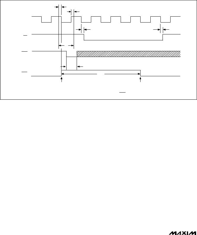
Figure 3. Initiating Conversions—At least 3 CLK cycles since end of previous conversion.
If the power supplies do not settle within the MAX194’s power-on delay (500ns minimum), power-up calibration may begin with supply voltages that differ from the final values and the converter may not be properly calibrated. If so, recalibrate the converter (pulse RESET low) before use. For best DC accuracy, calibrate the MAX194 any time there is a significant change in supply voltages, temperature, reference voltage, or clock characteristics (see External Clock section) because these parameters affect the DC offset. If linearity is the only concern, much larger changes in these parameters can be tolerated.
Because the calibration data is stored digitally, there is no need either to perform frequent conversions to maintain accuracy or to recalibrate if the MAX194 has been held in shutdown for long periods. However, recalibration is recommended if it is likely that supply voltages or ambient temperature has significantly changed since the previous calibration.
Digital Interface
The digital interface pins consist of BP/UP/SHDN, CLK, SCLK, EOC, CS, CONV, and RESET.
BP/UP/SHDN is a three-level input. Leave it floating to configure the MAX194’s analog input in bipolar mode (AIN = -VREF to VREF) or connect it high for a unipolar
input (AIN = 0V to VREF). Bringing BP/UP/SHDN low places the MAX194 in its 10µA shutdown mode.
A logic low on RESET halts MAX194 operation. The rising edge of RESET initiates calibration as described in
the Calibration section above.
Begin a conversion by bringing CONV low. The convert signal must be synchronized with CLK. The falling edge of CONV must occur during the period shown in Figures 3 and 4. When CLK is not directly controlled by your processor, two methods of ensuring synchronization are to drive CONV from EOC (continuous conversions) or to gate the conversion-start signal with the conversion clock so that CONV can go low only while CLK is low (Figure 5). Ensure that the maximum propagation delay through the gate is less than 40ns.
The MAX194 automatically ensures four CLK periods for track/hold acquisition. If, when CONV is asserted, at least three clock (CLK) cycles have passed since the end of the previous conversion, a conversion will begin on CLK’s next falling edge and EOC will go high on the following falling CLK edge (Figure 3). After conversion begins, additional convert start pulses are ignored. If, when convert is asserted, less than three clock cycles have passed, a conversion will begin on the fourth falling clock edge after the end of the previous conver-
_______________________________________________________________________________________ 7
14-Bit, 85ksps ADC with 10µA Shutdown
MAX194 |
tCC1 |
|
tCC2 |
|
|
CLK |
|
|
tCEL |
tCEH |
|
EOC |
|
|
|
|
|
|
* |
|
|
CONV |
|
|
tCW |
|
|
TRACK/HOLD |
tAQ |
|
CONVERSION |
CONVERSION |
|
ENDS |
BEGINS |
|
* THE FALLING EDGE OF CONV MUST OCCUR IN THIS REGION |
|
Figure 4. Initiating Conversions—Less than 3 CLK cycles since end of previous conversion.
sion and EOC will go high on the following CLK falling edge (Figure 4). CONV is ignored during conversions.
External Clock
The conversion clock (CLK) should have a duty cycle between 25% and 75% at 1.7MHz (the maximum clock frequency). For lower frequency clocks, ensure the minimum high and low times exceed 150ns. The minimum clock rate for accurate conversion is 125Hz for temperatures up to +70°C or 1kHz at +125°C due to leakage of the sampling capacitor array. In addition, CLK should not remain high longer than 50ms at tem-
peratures up to +70°C or 500µs at +125°C. If CLK is held high longer than this, RESET must be pulsed low
to initiate a recalibration because it is possible that state information stored in internal dynamic memory may be lost. The MAX194’s clock can be stopped indefinitely if it is held low.
If the frequency, duty cycle, or other aspects of the clock signal’s shape change, the offset created by coupling between CLK and the analog inputs (AIN and REF) changes. Recalibration corrects for this offset and restores DC accuracy.
SPI/QSPI are trademarks of Motorola Corp.
Output Data
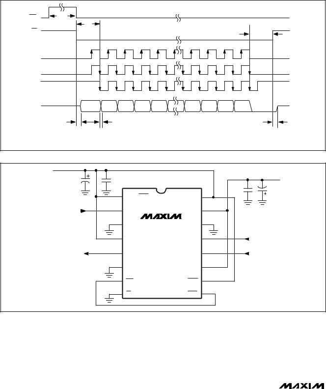
The conversion result is clocked out MSB first, formatted as 14 data bits plus two sub-LSBs. Serial data is available on DOUT only when CS is held low. Otherwise, DOUT is in a high-impedance state. There are two ways to read the data on DOUT. To read the data bits as they are determined (at the CLK clock rate), hold CS low during the conversion. To read results between conversions, hold CS low and clock SCLK at up to 5MHz.
If you read the serial data bits as they are determined (at the conversion-clock rate), EOC frames the data bits
(Figure 6). Conversion begins with the first falling CLK edge, after CONV goes low and the input signal has
been acquired. Data bits are shifted out of DOUT on subsequent falling CLK edges. Clock data in on CLK’s rising edge or, if the clock speed is greater than 1MHz, on the following falling edge of CLK to meet the maximum CLK-to-DOUT timing specification. See the
Operating Modes and SPI™/QSPI™ Interfaces section for additional information. Reading the serial data during the conversion results in the maximum conversion throughput, because a new conversion can begin immediately after the input acquisition period following the previous conversion.
8 _______________________________________________________________________________________

14-Bit, 85ksps ADC with 10µA Shutdown
START |
MAX194 |
|
CONV |
|
CLK |
START
CLK
CONV
MAX194
SEE DIGITAL INTERFACE SECTION
Figure 5. Gating CONV to Synchronize with CLK
CS |
|
|
|
|
|
|
|
|
|
|
CONV |
|
|
|
|
|
|
|
|
|
|
|
tCW |
|
|
|
|
|
|
|
|
|
CLK |
|
|
|
|
|
|
|
|
|
|
(CASE 1) |
|
|
|
|
|
|
|
|
|
|
CLK |
|
|
|
|
|
|
|
|
|
|
(CASE 2) |
|
|
tCEH |
|
|
|
|
|
tCEL |
|
EOC |
|
|
|
|
|
|
|
|||
|
|
|
|
|
|
|
|
|
||
|
tDV |
|
tCD |
|
|
|
|
|
|
|
DOUT |
B13 FROM PREVIOUS |
B13 |
B12 |
B11 |
B10 |
B0 |
S1 |
S0 |
B13 |
|
CONVERSION |
||||||||||
|
|
|
|
|
|
|
|
|
||
|
|
MSB |
|
|
LSB |
SUB-LSBs |
tDH |
|||
CONVERSION
BEGINS CONVERSION
ENDS
CASE 1: CLK IDLES LOW, DATA LATCHED ON RISING EDGE (CPOL = 0, CPHA = 0)
CASE 2: CLK IDLES LOW, DATA LATCHED ON FALLING EDGE (CPOL = 0, CPHA = 1)
NOTE: ARROWS ON CLK TRANSITIONS INDICATE LATCHING EDGE
Figure 6. Output Data Format, Reading Data During Conversion (Mode 1)
If you read the data bits between conversions, you can
1)count CLK cycles until the end of the conversion, or
2)poll EOC to determine when the conversion is finished, or
3)generate an interrupt on EOC’s falling edge.
Note that the MSB conversion result appears at DOUT after CS goes low but before the first SCLK pulse. Each subsequent SCLK pulse shifts out the next conversion
bit. The 15th SCLK pulse shifts out the sub-LSB (S0). Additional clock pulses shift out zeros.
Data is clocked out on SCLK’s falling edge. Clock data in on SCLK’s rising edge or, for clock speeds above 2.5MHz, on the following falling edge to meet the maximum SCLK-to-DOUT timing specification (Figure 7). The maximum SCLK speed is 5MHz. See the Operating Modes and SPI/QSPI Interfaces section for additional information. When the conversion clock is near its maxi-
_______________________________________________________________________________________ 9
MAX194
14-Bit, 85ksps ADC with 10µA Shutdown
EOC |
tCONV |
|
|
|
|
|
|
|
|
|
|
|
|
|
|
|
|
|
|
|
|
|
|
tCSS |
|
|
|
|
|
|
|
|
CS |
|
|
|
|
|
|
|
|
|
tCSH |
|
|
|
|
|
|
|
|
|
|
|
SCLK |
|
|
|
|
|
|
|
|
|
|
(CASE 1) |
|
|
|
|
|
|
|
|
|
|
SCLK |
|
|
|
|
|
|
|
|
|
|
(CASE 2) |
|
|
|
|
|
|
|
|
|
|
SCLK |
|
|
|
|
|
|
|
|
|
|
(CASE 3) |
|
|
|
|
|
|
|
|
|
|
DOUT |
|
B13 |
B12 |
B11 |
B10 |
B9 |
B1 |
B0 |
S1 |
S0 |
|
|
MSB |
|
|
|
|
|
LSB |
SUB-LSBs |
|
|
tDV |
|
|
tSD |
|
|
|
|
|
tDH |
CASE 1: SCLK IDLES LOW, DATA LATCHED ON RISING EDGE (CPOL = 0, CPHA = 0) |
|
|
|
|
||||||
CASE 2: SCLK IDLES LOW, DATA LATCHED ON FALLING EDGE (CPOL = 0, CPHA = 1) |
NOTE: ARROWS ON SCLK TRANSITIONS INDICATE LATCHING EDGE |
|||||||||
CASE 3: SCLK IDLES HIGH, DATA LATCHED ON FALLING EDGE (CPOL = 1, CPHA = 0) |
||||||||||
Figure 7. Output Data Format, Reading Data Between Conversions (Mode 2)
+5V |
|
|
|
|
|
|
10μF |
0.1μF |
|
|
|
|
-5V |
|
1 |
|
|
|
0.1μF |
10μF |
|
BP/UP/SHDN |
|
VDDA |
16 |
|
|
|
|
|
|
|
||
CONVERSION CLOCK |
2 |
CLK |
|
VSSA |
15 |
|
|
|
|
|
|||
|
3 |
SCLK |
MAX194 |
AGND |
14 |
|
|
|
|
|
|||
|
4 |
VDDD |
|
AIN |
13 |
ANALOG INPUT |
|
|
|
|
|||
|
5 |
DOUT |
|
REF |
12 |
REFERENCE (0V TO VDDA) |
|
|
|
|
|||
|
6 |
DGND |
|
VSSD |
11 |
|
|
|
|
|
|
||
|
7 |
EOC |
|
RESET |
10 |
|
|
|
|
|
|
||
|
8 |
CS |
|
CONV |
9 |
|
|
|
|
|
|
Figure 8. MAX194 in the Simplest Operating Configuration
mum (1.7MHz), reading the data after each conversion (during the acquisition time) results in lower throughput (about 70ksps max) than reading the data during conversions, because it takes longer than the minimum input acquisition time (four cycles at 1.7MHz) to clock 16 data bits at 5Mbps. After the data has been clocked
in, leave some time (about 1µs) for any coupled noise on AIN to settle before beginning the next conversion.
Whichever method is chosen for reading the data, conversions can be individually initiated by bringing CONV low, or they can occur continuously by connecting EOC to CONV. Figure 8 shows the MAX194 in its simplest operational configuration.
10 ______________________________________________________________________________________