

бакМИТ_КП2015 / Компоненты по вариантам / АЦП / MAX194
.pdf14-Bit, 85ksps ADC with 10µA Shutdown
Table 1. Low-ESR Capacitor Suppliers
COMPANY |
CAPACITOR |
FACTORY FAX [COUNTRY CODE] |
USA TELEPHONE |
|
|
|
|
|
|
Sprague |
595D series, |
[1]-603-224-1430 |
603-224-1961 |
|
592D series |
||||
|
|
|
||
|
|
|
|
|
AVX |
TPS series |
[1]-207-283-1941 |
800-282-4975 |
|
|
|
|
|
|
Sanyo |
OS-CON series, |
[81]-7-2070-1174 |
619-661-6835 |
|
MV-GX series |
||||
|
|
|
||
|
|
|
|
|
Nichicon |
PL series |
[1]-708-843-2798 |
708-843-7500 |
|
|
|
|
|
MAX194
BRIDGE |
+5V |
|
|
||
INSTRUMENTATION |
VDDA |
|
AMPLIFIER |
||
|
||
|
MAX194 |
|
|
AIN |
|
|
REF |
|
47μF |
0.1μF |
|
LOW |
||
CERAMIC |
||
ESR |
|
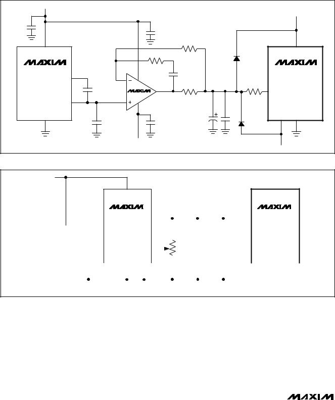
Figure 9. Ratiometric Measurement Without an Accurate Reference
__________Applications Information
Reference
The MAX194 reference voltage range is 0V to VDDA. When choosing the reference voltage, the MAX194’s equivalent input noise (40µVRMS in unipolar mode, 80µVRMS in bipolar mode) should be considered. Also, if VREF exceeds VDDA, errors will occur due to the internal protection diodes that will begin to conduct, so use caution when using a reference near VDDA (unless VREF and VDDA are virtually identical). VREF must never exceed its absolute maximum rating (VDDA + 0.3V).
The MAX194 needs a good reference to achieve its rated performance. The most important requirement is that the reference must present a low impedance to the REF input. This is often achieved by buffering the reference through an op amp and bypassing the REF input with a large (1µF to 47µF), low-ESR capacitor in parallel with a 0.1µF ceramic capacitor. Low-ESR capacitors are available from the manufacturers listed in Table 1.
The reference must drive the main conversion DAC capacitors as well as the capacitors in the calibration
DACs, all of which may be switching between GND and REF at the conversion clock frequency. The total capacitive load presented can exceed 1000pF and, unlike the analog input (AIN), REF is sampled continuously throughout the conversion.
The first step in choosing a reference circuit is to decide what kind of performance is required. This often suggests compromises made in the interests of cost and size. It is possible that a system may not require an accurate reference at all. If a system makes a ratiometric measurement such as Figure 9’s bridge circuit, any relatively noise-free voltage that presents a low impedance at the REF input will serve as a reference. The +5V analog supply suffices if you use a large, lowimpedance bypass capacitor to keep REF stable during switching of the capacitor arrays. Do not place a resistance between the +5V supply and the bypass capacitor, because it will cause linearity errors due to the dynamic REF input current, which typically ranges from 300µA to 400µA.
Figure 10 shows a more typical scheme that provides good AC accuracy. The MAX874’s initial accuracy can
______________________________________________________________________________________ 11
14-Bit, 85ksps ADC with 10µA Shutdown
MAX194 |
+15V |
|
|
|
|
|
|
|
|
|
|
|
|
|
|
|
|
|
|
+5V |
|
0.1mF |
|
|
|
|
0.1mF |
|
|
|
|
|
|
|
|
|
|
|
|
|
|
||
2 |
|
|
|
|
|
1k |
|
|
16 |
|
VIN |
|
|
|
|
2k |
|
|
|
VDDA |
|
|
|
|
|
|
|
1N914 |
|
|
||
|
|
|
|
|
|
|
|
|
||
|
|
|
|
|
|
|
|
|
|
|
|
MAX874 |
8 |
|
2 |
|
|
0.1mF |
|
MAX194 |
|
|
COMP |
|
7 |
|
|
|
|
|||
|
|
|
|
|
|
|
||||
|
|
|
|
|
|
|
|
|
|
|
|
|
|
1000pF |
|
|
6 |
|
10W |
REF |
|
|
|
|
|
|
|
|
|
|
||
|
|
|
|
|
MAX427 |
|
|
|
|
|
|
VOUT |
6 |
4.096V |
3 |
|
10W |
|
12 |
|
|
|
4 |
|
|
|
|
|||||
|
|
|
|
|
|
|
|
|
||
|
|
|
|
|
|
47mF |
0.1mF |
|
|
|
|
|
|
|
|
|
|
|
|
||
|
GND |
|
0.1mF |
|
|
0.1mF |
LOW |
|
VSSA |
AGND |
|
|
|
|
|
|
|
|
|||
|
4 |
|
|
|
ESR |
1N914 |
15 |
14 |
||
|
|
|
|
|
|
|||||
|
|
|
|
|
-15V |
|
|
|
|
|
|
|
|
|
|
|
|
|
|
-5V |
|
Figure 10. Typical Reference Circuit for AC Accuracy
VIN ³ 8V
2
IN
|
|
|
|
|
|
|
|
|
|
|
|
|
|
|
|
|
|
|
|
|
|
|
|
|
|
|
|
|
|
|
|
|
|
|
|
|
|
|
|
|
|
|
|
|
|
|
MAX6241 |
OUT |
6 |
|
|
|
|
|
12 |
|
|
MAX194 |
|
||||||||||||
|
|
|
|
|
|
|
|
|
|
|
|
|
|
|
|
|
|
|
|
REF |
|
||||||||||||||
2.2mF |
|
|
|
|
|
|
|
|
|
|
|
|
|
|
|
|
|
|
|
|
|
|
|
|
|
||||||||||
|
|
|
|
|
|
|
|
|
|
|
|
|
|
|
|
|
|
|
|
|
|
|
|
|
|
|
|
|
|
|
|
|
|
|
|
|
|
|
|
|
|
|
|
|
|
|
|
|
|
|
|
|
|
|
|
|
|
|
|
|
|
|
|||||||||
|
3 |
|
NR |
GND |
TRIM |
5 |
|
10k |
|
|
2.2mF |
|
|
0.1mF |
|
AGND |
|
||||||||||||||||||
|
|
|
|
|
|
|
|
|
|||||||||||||||||||||||||||
|
|
|
|
|
|
||||||||||||||||||||||||||||||
|
|
|
|
1mF |
|
|
|
|
|
|
|
|
|
|
|
|
|
|
|
|
|
|
|||||||||||||
|
|
|
|
|
|
|
|
|
|
|
|
|
|
|
|
|
|
|
|
|
|
|
|
|
|
|
|
|
|||||||
|
|
|
|
|
|
|
|
|
|
|
|
|
|
|
|
|
|
|
|
|
|
|
|
|
|
|
|
|
|||||||
|
|
|
|
|
|
|
|
|
|
|
4 |
|
|
|
|
|
|
|
|
|
|
|
|
|
|
|
|
|
|
|
|
14 |
|
||
|
|
|
|
|
|
|
|
|
|
|
|
|
|
|
|
|
|
|
|
|
|
|
|
|
|
|
|
|
|
|
|
|
|
|
|
|
|
|
|
|
|
|
|
|
|
|
|
|
|
|
|
|
|
|
|
|
|
|
|
|
|
|
|
|
|
|
|
|
|
|
|
|
|
|
|
|
|
|
|
|
|
|
|
|
|
|
|
|
|
|
|
|
|
|
|
|
|
|
|
|
|
|
|
|
|
|
|
|
|
|
|
|
|
|
|
|
|
|
|
|
|
|
|
|
|
|
|
|
|
|
|
|
|
|
|
|
|
|
|
|
|
|
|
Figure 11. High-Accuracy Reference
be improved by trimming, but the drift is too great to provide good stability over temperature. The MAX427 buffer provides the necessary drive current to stabilize the REF input quickly after capacitance changes.
The reference inaccuracies contribute additional fullscale error. A reference with less than 1⁄214 total error (61 parts per million) over the operating temperature range is required to maintain full 14-bit accuracy. The MAX6241 achieves a drift specification of 1ppm/°C
(typ) and easily drives the REF input directly. This allows large temperature changes with less than 1LSB error. While the MAX6241’s initial-accuracy specification (0.02%) results in a maximum error of about ±4LSB, the reference voltage can be trimmed or the offset can be corrected in software if absolute DC accuracy is essential. Figure 11’s circuit provides outstanding temperature stability and also provides excellent DC accuracy if the initial error is corrected.
12 ______________________________________________________________________________________
14-Bit, 85ksps ADC with 10µA Shutdown
+5V
VDDA
+15V
MAX194
10Ω
AIN
INPUT |
|
|
|
|
|
|
1N914 |
|
|
|||
SIGNAL |
|
|
|
|
|
|
|
|
|
|||
|
|
|
DIODE |
|
|
|||||||
|
|
|
|
|
|
|
|
|
||||
|
|
|
|
|
|
|
CLAMPS |
VSSA |
||||
|
|
|
|
|
|
|
|
|
|
|
||
|
|
|
|
|
|
-15V |
|
|
||||
|
|
|
|
|
|
|||||||
|
|
|
|
|
|
|
|
|
|
|
|
|
|
|
|
|
|
|
|
|
|
|
|
|
|
|
|
|
|
|
|
|
|
|
|
|
-5V |
|
Figure 12. Analog Input Protection for Overvoltage or Improper Supply Sequence
MAX194
A0 A1
IN1
|
|
|
|
|
|
|
|
|
|
|
|
|
|
|
|
|
|
|
|
|
|
|
|
|
|
|
|
|
|
|
|
|
|
IN2 |
4-TO-1 |
|
|
|
|
|
|
|
|
|
|
|
|
MAX194 |
|
|
|
|
|
|
|
|
|
|
|
|
|
|
|
|
|
||
|
MUX |
|
|
|
|
|
|
|
|
|
|
|
|
|
|
|
IN3 |
OUT |
|
|
|
|
|
|
|
|
|
|
AIN |
|
|||
|
|
|
|
|
|
|
|
|
|
|
||||||
IN4 |
|
|
|
|
|
|
|
|
|
|
|
|
|
|
|
|
|
|
|
|
|
|
|
|
|
|
EOC |
|
|||||
|
|
|
|
|
|
|
|
|
|
|
|
|||||
CLK
CONVERSION |
AQUISITION |
EOC
A0
A1
CHANGE MUX INPUT HERE
Figure 13. Change multiplexer input near beginning of conversion to allow time for slewing and settling.
______________________________________________________________________________________ 13
MAX194
14-Bit, 85ksps ADC with 10µA Shutdown
|
|
1k |
|
+15V |
+5V |
|
0.1μF |
1000pF |
2 |
7 |
1N914 |
|
||
|
6 |
10Ω |
|
AIN |
|
|
MAX400 |
|
3 |
100Ω |
|
IN |
4 |
1N914 |
|
||
|
|
|
|
0.1μF |
1.0μF |
|
|
|
|
-15V |
-5V |
Figure 14. MAX400 Drives AIN for Low-Frequency Use
|
|
1k |
|
|
|
|
|
+15V |
|
|
+15V |
|
+5V |
|
|
|
|
|
||
|
0.1μF |
100pF |
|
|
0.1μF |
1N914 |
2 |
7 |
|
|
|
1 |
|
|
|
|
|
|||
|
6 |
|
2 |
ELANTEC |
7 |
10Ω |
|
|
AIN |
||||
|
MAX427 |
|
|
EL2003 |
|
|
3 |
1k |
|
|
|
||
IN |
4 |
|
|
|
4 |
1N914 |
|
|
|
|
|
0.0033μF |
|
|
0.1μF |
|
|
|
0.1μF |
|
|
-15V |
|
|
-15V |
|
-5V |
Figure 15. AIN Buffer for AC/DC Use
REF and AIN Input Protection
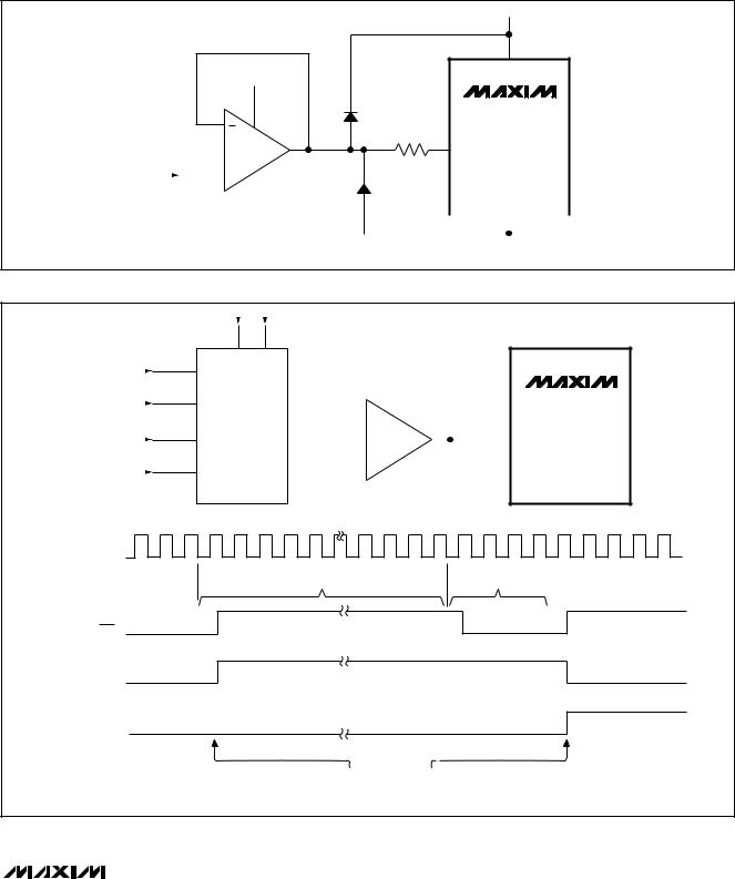
The REF and AIN signals should not exceed the MAX194 supply rails. If this can occur, diode clamp the signal to the supply rails. Use silicon diodes and a 10Ω current-limiting resistor (Figures 10 and 12) or Schottky diodes without the resistor.
When using the current-limiting resistor, place the resistor between the appropriate input (AIN or REF) and any bypass capacitor. While this results in AC transients at the input due to dynamic input currents, the transients settle quickly and do not affect conversion results. Improperly placing the bypass capacitor directly at the input forms an RC lowpass filter with the current-limiting resistor, which averages the dynamic input current and causes linearity errors.
Analog Input
The MAX194 uses a capacitive DAC that provides an inherent track/hold function. The input impedance is typically 30Ω in series with 250pF in unipolar mode and 50Ω in series with 125pF in bipolar mode.
Input Range
The analog input range can be either unipolar (0V to VREF) or bipolar (-VREF to VREF), depending on the state of the BP/UP/SHDN pin (see Digital Interface section). The reference range is 0V to VDDA. When choosing the reference voltage, the equivalent MAX194 input noise (40µVRMS in unipolar mode, 80µVRMS in bipolar mode) should be considered.
14 ______________________________________________________________________________________
14-Bit, 85ksps ADC with 10µA Shutdown
|
510Ω |
|
|
+5V |
|
|
|
0.1μF |
2 |
7 |
|
|
6 |
22Ω |
|
|
 AIN
AIN
3 |
MAX410 |
|
|
|
|
|
|||||||||||||||
IN |
|
|
|
|
|
|
4 |
|
|
|
|
|
|
|
|
|
|
|
|
|
|
|
|
|
|
|
|
|
|
|
|
|
|
|
|
|
|
|
|
|
|
||
|
|
|
|
|
|
|
|
|
|
|
|
|
|
|
|
|
|
|
|
||
|
|
|
|
|
|
|
|
|
|
|
|
|
|
0.1μF |
|
|
|
|
|
0.01μF |
|
|
|
|
|
|
|
|
|
|
|
|
|
|
|
|
|
|
|
|
|||
|
|
|
|
|
|
|
|
|
|
|
|
|
|
|
|
|
|
|
|||
|
|
|
|
|
|
|
|
|
|
|
|
|
|
|
|
|
|
|
|
|
|
|
|
|
|
|
|
-5V |
|
|
|
|
|
|
|
|
|
|
|
||||
|
|
|
|
|
|
|
|
|
|
|
|
|
|||||||||
Figure 16. ±5V Buffer for AC/DC Use Has ±3.5V Swing
Input Acquisition and Settling
Four conversion-clock periods are allocated for acquiring the input signal. At the highest conversion rate, four clock periods is 2.4µs. If more than three clock cycles have occurred since the end of the previous conversion, conversion begins on the next falling clock edge after CONV goes low. Otherwise, bringing CONV low begins a conversion on the fourth falling clock edge after the previous conversion. This scheme ensures the minimum input acquisition time is four clock periods.
Most applications require an input buffer amplifier. If the input signal is multiplexed, the input channel should be switched near the beginning of a conversion, rather than near the end of or after a conversion (Figure 13). This allows time for the input buffer amplifier to respond to a large step change in input signal. The input amplifier must have a high enough slew rate to complete the required output voltage change before the beginning of the acquisition time.
At the beginning of acquisition, the capacitive DAC is connected to the amplifier output, causing some output disturbance. Ensure that the sampled voltage has settled to within the required limits before the end of the acquisition time. If the frequency of interest is low, AIN can be bypassed with a large enough capacitor to charge the capacitive DAC with very little change in voltage (Figure 14). However, for AC use, AIN must be driven by a wideband buffer (at least 10MHz), which must be stable with the DAC’s capacitive load (in parallel with any AIN bypass capacitor used) and also must settle quickly (Figure 15 or 16).
Digital Noise
Digital noise can easily be coupled to AIN and REF. The conversion clock (CLK) and other digital signals
that are active during input acquisition contribute noise to the conversion result. If the noise signal is synchronous to the sampling interval, an effective input offset is produced. Asynchronous signals produce random noise on the input, whose high-frequency components may be aliased into the frequency band of interest. Minimize noise by presenting a low impedance (at the frequencies contained in the noise signal) at the inputs. This requires bypassing AIN to AGND, or buffering the input with an amplifier that has a small-signal bandwidth of several megahertz, or preferably both. AIN has a bandwidth of about 16MHz.
Offsets resulting from synchronous noise (such as the conversion clock) are canceled by the MAX194’s calibration scheme. However, because the magnitude of the offset produced by a synchronous signal depends on the signal’s shape, recalibration may be appropriate if the shape or relative timing of the clock or other digital signals change, as might occur if more than one clock signal or frequency is used.
Distortion
Avoid degrading dynamic performance by choosing an amplifier with distortion much less than the MAX194’s THD (-90dB, or 0.0032%) at frequencies of interest. If the chosen amplifier has insufficient common-mode rejection, which results in degraded THD performance, use the inverting configuration (positive input grounded) to eliminate errors from this source. Low tempera- ture-coefficient, gain-setting resistors reduce linearity errors caused by resistance changes due to self-heat- ing. Also, to reduce linearity errors due to finite amplifier gain, use an amplifier circuit with sufficient loop gain at the frequencies of interest (Figures 14, 15, 16).
MAX194
______________________________________________________________________________________ 15
MAX194
14-Bit, 85ksps ADC with 10µA Shutdown
QSPI |
MAX194 |
|
|
PCS0 |
CS |
|
CONV |
SCK |
CLK |
MISO |
DOUT |
GPT |
SCLK |
|
|
*OC3 |
BP/UP/SHDN |
*IC1 |
EOC |
*OC2 |
RESET |
*THE USE OF THESE SIGNALS ADDS FLEXIBILITY AND FUNCTIONALITY BUT IS NOT REQUIRED TO IMPLEMENT THE INTERFACE.
Figure 17. MAX194 Connection to QSPI Processor Clocking Data Out During Conversions
DC Accuracy
If DC accuracy is important, choose a buffer with an offset much less than the MAX194’s maximum offset (±1 LSB = ±488µV for a ±4V input range), or whose offset can be trimmed while maintaining good stability over the required temperature range.
Recommended Circuits
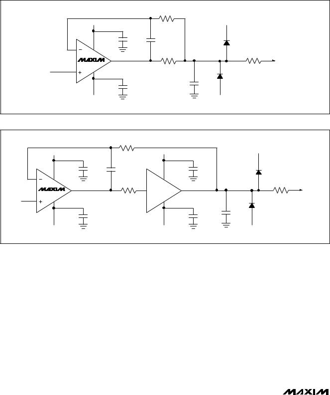
Figure 14 shows a good circuit for DC and low-frequen- cy use. The MAX400 has very low offset (10µV) and drift (0.2µV/°C), and low voltage noise (10nV/√Hz) as well. However, its gain-bandwidth product (GBW) is much too low to drive AIN directly, so the analog input is bypassed to present a low impedance at high frequencies. The large bypass capacitor is isolated from the amplifier output by a 100Ω resistor, which provides additional noise filtering. Since the ±15V supplies exceed the AIN range, add protection diodes at AIN.
Figure 15 shows a wide-bandwidth amplifier (MAX427) driving a wideband video buffer, which is capable of driving AIN and a small bypass capacitor (for noise reduction) directly. The video buffer is inside the MAX427’s feedback loop, providing good DC accuracy, while the buffer’s low output impedance and high current capabil-
ity provide good AC performance. AIN is diodeclamped to the ±5V rails to prevent overvoltage. The MAX427’s 15µV maximum offset voltage, 0.8µV/°C maximum drift, and less than 5nV/√Hz noise specifications make this an excellent choice for AC/DC use.
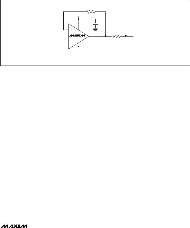
If ±15V supplies are unavailable, Figure 16’s circuit works very well with the ±5V analog supplies used by the MAX194. The MAX410 has a minimum ±3.5V commonmode input range, with a similar output voltage swing, which allows use of a reference voltage to 3.5V. The offset voltage (250µV), drift (1µV/°C), unity-gain bandwidth (28MHz), and low voltage noise (2.4nV/√Hz) are appropriate for 14-bit performance. The 0.01µF bypass capacitor improves the noise performance.
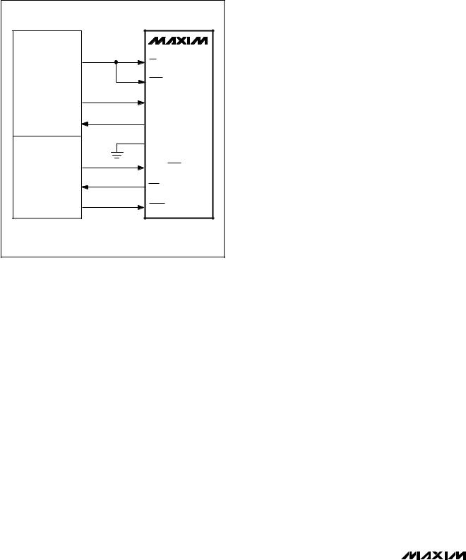
Operating Modes and SPI/QSPI Interfaces
The two basic interface modes are defined according to whether serial data is received during the conversion (clocked with CLK, SCLK unused) or in bursts between conversions (clocked with SCLK). Each mode is presented interfaced to a QSPI processor, but is also compatible with SPI.
Mode 1 (Simultaneous Conversion and Data Transfer)
In this mode, each data bit is read from the MAX194 during the conversion as it is determined. SCLK is grounded and CLK is used as both the conversion clock and the serial data clock. Figure 17 shows a QSPI processor connected to the MAX194 for use in this mode and Figure 18 is the associated timing diagram.
In addition to the standard QSPI interface signals, gener-
al I/O lines are used to monitor EOC and to drive BP/UP/SHDN and RESET. The two general output pins
may not be necessary for a given application and, if I/O lines are unavailable, the EOC connection can be omitted as well.
The EOC signal is monitored during calibration to determine when calibration is finished and before beginning a conversion to ensure the MAX194 is not in mid-con- version, but it is possible for a system to ignore EOC completely. On power-up or after pulsing RESET low, the µP must provide 14,000 CLK cycles to complete the calibration sequence (Figure 2). One way to do this is to toggle CLK and monitor EOC until it goes low, but it is possible to simply count 14,000 CLK cycles to complete the calibration. Similarly, it is unnecessary to check the status of EOC before beginning a conversion if you are sure the last conversion is complete. This can be done by ensuring that every conversion consists of at least 20 CLK cycles.
16 ______________________________________________________________________________________

14-Bit, 85ksps ADC with 10µA Shutdown
CS, CONV |
|
|
|
|
|
|
MAX194 |
|
CLK |
|
|
|
|
|
|
||
|
|
|
|
|
|
|
||
EOC |
|
|
|
|
|
|
|
|
DOUT |
B13 FROM PREVIOUS |
B13 |
B12 |
B0 |
S1 |
S0 |
B13 |
|
CONVERSION |
||||||||
|
|
|
|
|
|
|
||
tDV |
|
tCD |
|
|
|
|
tDH |
|
|
|
|
|
|
|
|||
DATA LATCHED: |
|
|
|
|
|
|
|
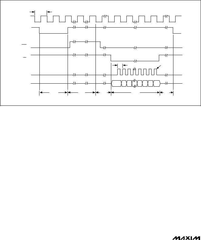
Figure 18. Timing Diagram for Circuit of Figure 17
QSPI |
|
MAX194 |
|
|
|
|
PCS0 |
CS |
|
SCK |
SCLK |
|
MISO |
DOUT |
GPT |
OC3 |
BP/UP/SHDN |
|
IC1 |
EOC |
|
OC2 |
RESET |
|
|
CONV |
IC3 |
|
CLK |
|
|
74HC32 |
|
|
1.7MHz |
|
1.3μs |
|
START |
|
|
Figure 19. MAX194 Connection to QSPI Processor Clocking Data Out with SCLK Between Conversions
MicroWire is a trademark of National Semiconductor Corp.
Data is clocked out of the MAX194 on CLK’s falling edge and can be clocked into the µP on the rising edge or the following falling edge. If you clock data in on the rising edge (SPI/QSPI with CPOL = 0 and CPHA = 0; standard MicroWire™: Hitachi H8), the maximum CLK rate is given by:
fCLK(max) |
= 1/ 2 |
· |
æ |
|
1 |
ö |
ç |
|
|
÷ |
|||
|
|
|||||
|
|
|
è tCD |
+ tSD ø |
||
where tCD is the MAX194’s CLK-to-DOUT valid delay and tSD is the data setup time for your µP.
If clocking data in on the falling edge (CPOL = 0, CPHA = 1), the maximum CLK rate is given by:
1 fCLK(max) = tCD + tSD
Do not exceed the maximum CLK frequency given in the Electrical Characteristics table. To clock data in on the falling edge, your processor hold time must not exceed tCD minimum (100ns).
While QSPI can provide the required 20 CLK cycles as two continuous 10-bit transfers, SPI is limited to 8-bit transfers. This means that with SPI, a conversion must consist of three 8-bit transfers. Ensure that the pauses between 8-bit operations at your selected clock rate are short enough to maintain a 20ms or shorter conversion time, or the leakage of the capacitive DAC may cause errors.
______________________________________________________________________________________ 17
14-Bit, 85ksps ADC with 10µA Shutdown
MAX194 |
588ns |
|
|
|
|
|
|
|
CLK |
|
|
|
|
|
|
|
|
START |
|
|
|
|
|
|
|
|
|
|
|
|
|
|
|
|
|
|
EOC |
|
|
|
|
|
|
|
|
CS |
|
|
|
|
|
|
|
|
|
|
|
239ns |
|
|
|
4.19MHz |
|
SCLK |
|
|
|
|
|
|
|
|
DOUT |
|
B13 |
B12 B11 |
B1 |
B0 |
S1 |
S0 |
|
|
CONVERSION TIME |
|
|
|
|
|
4μs |
|
1.3μs |
9.4μs |
17μs |
5.1μs |
|
|
|
Figure 20. Timing Diagram for Circuit of Figure 19
Complete source code for the Motorola 68HC16 and the MAX194 evaluation kit (EV kit) using this mode is available in the MAX194 EV kit manual.
Mode 2 (Asynchronous Data Transfer)
This mode uses a conversion clock (CLK) and a serial clock (SCLK). The serial data is clocked out between conversions, which reduces the maximum throughput for high CLK rates, but may be more convenient for some applications. Figure 19 is a block diagram with a QSPI processor (Motorola 68HC16) connected to the MAX194. Figure 20 shows the associated timing diagram. Figure 21 gives an assembly language listing for this arrangement.
An OR gate is used to synchronize the “start” signal to the asynchronous CLK, as described in the External Clock section. As with Mode 1, the QSPI processor must run CLK during calibration and either count CLK cycles or, as is done here, monitor EOC to determine when calibration is complete. Also, EOC is polled by the µP to determine when a conversion result is available. When EOC goes low, data is clocked out at the highest QSPI data rate (4.19Mbps). After the data is transferred, a new conversion can be initiated whenever desired.
The timing specification for SCLK-to-DOUT valid (tSD) imposes some constraints on the serial interface. At SCLK rates up to 2.5Mbps, data is clocked out of the MAX194 by a falling edge of SCLK and may be clocked into the µP by the next rising edge (CPOL = 0, CPHA = 0). For data rates greater than 2.5Mbps (or for lower rates, if desired) it is necessary to clock data out of the MAX194 on SCLK’s falling edge and to clock it into the µP on SCLK’s next falling edge (CPOL = 0, CPHA = 1). Also, your processor hold time must not exceed tSD minimum (20ns). As with CLK in mode 1, maximum SCLK rates may not be possible with some interface specifications that are subsets of SPI.
Supplies, Layout, Grounding and Bypassing
For best system performance, use printed circuit boards with separate analog and digital ground planes. Wirewrap boards are not recommended. The two ground planes should be tied together at the low-impedance power-supply source and at the MAX194, as shown in Figure 22. If the analog and digital supplies come from the same source, isolate the digital supply from the analog supply with a low-value resistor (10Ω ).
18 ______________________________________________________________________________________
14-Bit, 85ksps ADC with 10µA Shutdown
MAX194
Figure 21. MAX194 Code Listing for 68HC16 Module and Circuit of Figure 19
______________________________________________________________________________________ 19
14-Bit, 85ksps ADC with 10µA Shutdown
MAX194
Figure 21. MAX194 Code Listing for 68HC16 Module and Circuit of Figure 19 (continued)
20 ______________________________________________________________________________________