

бакМИТ_КП2015 / Компоненты по вариантам / АЦП / MAX1165
.pdf19-2551; Rev 2; 8/08
Low-Power, 16-Bit Analog-to-Digital Converters
with Parallel Interface
General Description
The MAX1165/MAX1166 16-bit, low-power, successiveapproximation analog-to-digital converters (ADCs) feature automatic power-down, factory-trimmed internal clock, and a 16-bit wide (MAX1165) or byte wide (MAX1166) parallel interface. The devices operate from a single +4.75V to +5.25V analog supply and a +2.7V to +5.25V digital supply.
The MAX1165/MAX1166 use an internal 4.096V reference or an external reference. The MAX1165/MAX1166 consume only 1.8mA at a sampling rate of 165ksps with external reference and 2.7mA with internal reference. AutoShutdown™ reduces supply current to 0.1mA at 10ksps.
The MAX1165/MAX1166 are ideal for high-perfor- mance, battery-powered, data-acquisition applications. Excellent dynamic performance and low power consumption in a small package make the MAX1165/ MAX1166 ideal for circuits with demanding power consumption and space requirements.
The 16-bit wide MAX1165 is available in a 28-pin TSSOP package and the byte wide MAX1166 is available in a 20-pin TSSOP package. Both devices are available in either the 0°C to +70°C commercial, or the -40°C to +85°C extended temperature range.
AutoShutdown is a trademark of Maxim Integrated Products, Inc.
Applications
Temperature Sensor/Monitor
Industrial Process Control
I/O Boards
Data-Acquisition Systems
Cable/Harness Tester
Accelerometer Measurements
Digital Signal Processing
Pin Configurations and Functional Diagram appear at end of data sheet.
Features
♦16-Bit Wide (MAX1165) and Byte Wide (MAX1166) Parallel Interface
♦High Speed: 165ksps Sample Rate
♦Accurate: ±2.5 LSB INL, 16 Bit No Missing Codes
♦4.096V, 25ppm/°C Internal Reference
♦External Reference Range: +3.8V to +5.25V
♦Single +4.75V to +5.25V Analog Supply Voltage
♦+2.7V to +5.25V Digital Supply Voltage
♦Low Supply Current
1.8mA (External Reference)
2.7mA (Internal Reference)
0.1µA (10ksps, External Reference)
♦ Small Footprint
28-Pin TSSOP Package (16-Bit Wide)
20-Pin TSSOP Package (Byte Wide)
Ordering Information
PART |
TEMP RANGE |
PIN- |
INL |
|
PACKAGE |
||||
|
|
|
||
MAX1165ACUI |
0°C to +70°C |
28 TSSOP |
±2 |
|
MAX1165BCUI |
0°C to +70°C |
28 TSSOP |
±2 |
|
MAX1165CCUI |
0°C to +70°C |
28 TSSOP |
±4 |
|
MAX1165AEUI |
-40°C to +85°C |
28 TSSOP |
±2.5 |
|
MAX1165BEUI |
-40°C to +85°C |
28 TSSOP |
±2.5 |
|
MAX1165CEUI |
-40°C to +85°C |
28 TSSOP |
±4 |
|
|
|
|
|
Ordering Information continued at end of data sheet.
Typical Operating Circuit
|
|
|
|
|
|
|
|
+5V ANALOG |
|
|
|
+5V DIGITAL |
|
|
|
|
|
|
|
|
||||||||||||||||||
|
0.1 F |
|
|
|
|
|
|
|
|
|
|
|
|
|
|
|
|
|
|
|
|
|
|
|
0.1 F |
|
|
|
|
|||||||||
|
|
|
|
|
|
|
|
|
|
|
|
|
|
|
|
|
|
|
|
|
|
|
|
|
|
|
|
|
||||||||||
|
|
|
|
|
|
|
|
|
|
|
|
|
|
|
|
|
|
|
|
|
|
|
|
|
|
|
|
|
|
|||||||||
|
|
|
|
|
|
|
|
|
|
|
|
|
|
|
|
|
|
|
|
|
|
|
|
|
|
|
|
|
|
|||||||||
|
|
|
|
|
|
|
|
|
|
|
|
|
|
|
|
|
|
|
|
|
|
|
|
|
|
|
|
|
|
|
P DATA |
|
|
|
|
|||
|
|
|
|
|
|
|
|
|
|
|
|
|
|
|
|
|
|
|
|
|
|
|
|
|
|
|
|
|
|
|
|
|
|
|
||||
|
|
|
|
|
|
|
|
|
|
|
|
|
|
|
|
|
|
|
|
|
|
|
|
|
|
|
|
|
|
|
|
|
|
|
||||
|
|
|
|
|
|
|
|
|
|
|
|
|
|
|
|
|
|
|
|
|
|
|
|
|
|
|
|
|
|
|
|
|
|
|
||||
|
|
|
|
|
|
|
|
|
|
|
|
|
|
|
|
|
|
|
|
|
|
|
|
|
|
|
|
|
|
|
BUS |
|
|
|
|
|||
|
|
|
|
|
|
|
|
|
|
|
AVDD |
|
|
|
|
|
|
|
DVDD |
|
|
|
|
|
|
|
|
|||||||||||
ANALOG INPUT |
|
|
|
|
|
|
AIN |
|
|
|
|
|
|
|
|
D0–D15 |
|
|
|
|
|
|
|
|
||||||||||||||
|
|
|
|
|
|
|
|
|
|
|
|
|
|
|
|
|
|
|
|
|
|
|
|
|
|
|
|
|
|
|||||||||
|
|
|
|
|
|
|
|
|
|
|
|
|
|
|
|
|
|
|
|
|
|
|
|
|
|
|
|
|
|
|
|
|
|
|
|
|
||
|
|
|
|
|
|
|
|
|
|
|
|
|
|
|
|
|
|
|
|
|
|
|
|
|
|
|
|
|
|
|
|
|
|
|
|
|
|
|
|
|
|
|
|
|
|
|
|
|
|
|
MAX1165 |
|
|
|
|
|
|
|
|
|
|
|
|
|
|
|
|
|
|
||||||||
|
|
|
|
|
|
|
|
|
|
|
|
|
|
|
EOC |
|
|
|
|
|
|
|
|
|||||||||||||||
|
|
|
|
|
|
|
R/C |
|
|
|
|
|
|
|
|
|
|
|
|
|
|
|
|
|
|
|||||||||||||
|
|
|
|
|
|
|
|
|
|
|
|
|
|
|
|
|
|
REF |
|
|
|
|
|
|
|
|
||||||||||||
|
|
|
|
|
|
|
|
|
|
|
|
|
|
|
|
|
|
|
|
|
|
|
|
|
|
|||||||||||||
|
|
|
|
|
|
|
|
CS |
|
|
|
|
|
|
|
|
|
REFADJ |
|
|
|
|
|
|
|
|
||||||||||||
|
|
|
|
|
|
|
|
|
|
|
|
|
|
|
|
|
|
|
|
|
|
|
||||||||||||||||
|
|
|
|
|
|
|
RESET |
|
|
|
|
|
|
|
|
|
|
|
|
|
|
|
|
|||||||||||||||
|
|
|
|
|
|
|
AGND DGND |
0.1 F |
|
|
|
|
|
4.7 F |
||||||||||||||||||||||||
|
|
|
|
|
|
|
|
|
|
|
|
|||||||||||||||||||||||||||
|
|
|
|
|
|
|
|
|
|
|
|
|
|
|
|
|
|
|
||||||||||||||||||||
|
|
|
|
|
|
|
|
|
|
|
|
|
|
|
|
|
|
|
||||||||||||||||||||
|
|
|
|
|
|
|
|
|
|
|
|
|
|
|
|
|
|
|
|
|
|
|
|
|
|
|
|
|
|
|
|
|
|
|
|
|
|
|
|
|
|
|
|
|
|
|
|
|
|
|
|
|
|
|
|
|
|
|
|
|
|
|
|
|
|
|
|
|
|
|
|
|
|
|
|
|
|
|
|
|
|
|
|
|
|
|
|
|
|
|
|
|
|
|
|
|
|
|
|
|
|
|
|
|
|
|
|
|
|
|
|
|
|
|
|
|
|
|
|
|
|
|
|
|
|
|
|
|
|
|
|
|
|
|
|
|
|
|
|
|
|
|
|
|
|
|
|
|
|
|
|
|
|
|
|
|
|
|
|
|
|
|
|
|
|
|
|
|
|
|
|
|
|
|
|
|
|
|
|
|
|
|
|
|
|
|
|
|
|
|
|
|
|
|
|
|
|
|
|
|
|
|
|
|
|
|
|
|
|
|
|
|
|
|
|
|
|
|
|
|
|
|
|
|
|
|
|
|
|
|
|
|
|
MAX1165/MAX1166
________________________________________________________________ Maxim Integrated Products 1
For pricing delivery, and ordering information please contact Maxim Direct at 1-888-629-4642, or visit Maxim’s website at www.maxim-ic.com.

MAX1165/MAX1166
Low-Power, 16-Bit Analog-to-Digital Converter with Parallel Interface
ABSOLUTE MAXIMUM RATINGS
AVDD to AGND ......................................................... |
|
- 0.3V to +6V |
DVDD to DGND ........................................ |
-0.3V to (AVDD + 0.3V) |
|
AGND to DGND..................................................... |
|
- 0.3V to +0.3V |
AIN, REF, REFADJ to AGND.................... |
-0.3V to (AVDD + 0.3V) |
|
CS, HBEN, R/C, RESET to DGND ............................ |
|
- 0.3V to +6V |
Digital Output (D15–D0, EOC) |
|
|
to DGND .............................................. |
-0.3V to (DVDD + 0.3V) |
|
Maximum Continuous Current Into Any Pin |
........................50mA |
|
Continuous Power Dissipation (TA = +70°C) |
|
|
20-Pin TSSOP (derate 10.9mW/°C above+70°C) ........ |
879mW |
|
28-Pin TSSOP (derate 12.8mW/°C above +70°C) ..... |
1026mW |
|
Operating Temperature Ranges |
|
|
MAX116_ _CU_................................................... |
0°C to +70°C |
|
MAX116_ _EU_ ................................................ |
-40°C to +85°C |
|
Storage Temperature Range ............................. |
-65°C to +150°C |
|
Junction Temperature ...................................................... |
|
+150°C |
Lead Temperature (soldering, 10s) ................................. |
|
+300°C |
Stresses beyond those listed under “Absolute Maximum Ratings” may cause permanent damage to the device. These are stress ratings only, and functional operation of the device at these or any other conditions beyond those indicated in the operational sections of the specifications is not implied. Exposure to absolute maximum rating conditions for extended periods may affect device reliability.
ELECTRICAL CHARACTERISTICS
(AVDD = DVDD = +5V, external reference = +4.096V, CREF = 4.7µF, CREFADJ = 0.1µF, TA = TMIN to TMAX, unless otherwise noted. Typical values are at TA = +25°C.)
PARAMETER |
SYMBOL |
|
CONDITIONS |
|
MIN |
TYP |
MAX |
UNITS |
|
|
|
|
|
|
|
|
|
|
|
DC ACCURACY |
|
|
|
|
|
|
|
|
|
Resolution |
N |
|
|
|
|
16 |
|
|
Bits |
|
|
|
|
|
|
|
|
|
|
|
|
|
|
MAX116_A |
|
-2.5 |
|
+2.5 |
|
|
|
TA = -40°C |
|
|
|
|
|
|
|
|
|
|
MAX116_B |
|
-2.5 |
|
+2.5 |
|
|
|
|
|
|
MAX116_C |
|
-4 |
|
+4 |
|
Relative Accuracy |
|
|
|
MAX116_A |
|
-2 |
|
+2 |
|
INL |
TA = 0°C |
|
|
|
|
|
|
|
|
|
MAX116_B |
|
-2 |
|
+2 |
LSB |
|||
(Note 1) |
|
|
|
||||||
|
|
|
MAX116_C |
|
-4 |
|
+4 |
|
|
|
|
|
|
|
|
|
|||
|
|
|
|
|
|
|
|
|
|
|
|
|
|
MAX116_A |
|
-2 |
|
+2 |
|
|
|
TA = +85°C |
|
|
|
|
|
|
|
|
|
|
MAX116_B |
|
-2 |
|
+2 |
|
|
|
|
|
|
MAX116_C |
|
-4 |
|
+4 |
|
|
|
|
|
No missing |
MAX116_A |
-1 |
|
+2 |
|
|
|
TA = -40°C |
|
codes |
MAX116_B |
-1 |
|
+2 |
|
|
|
|
|
MAX116_C |
|
-2 |
|
+2 |
|
|
|
|
|
|
|
|
|
|
|
|
|
|
|
No missing |
MAX116_A |
-1 |
|
+1.5 |
|
Differential Nonlinearity |
DNL |
TA = 0°C |
|
codes |
MAX116_B |
-1 |
|
+1.5 |
LSB |
|
|
|
|
MAX116_C |
|
-2 |
|
+2 |
|
|
|
|
|
|
|
|
|
|
|
|
|
|
|
No missing |
MAX116_A |
-1 |
|
+1 |
|
|
|
TA = +85°C |
|
codes |
MAX116_B |
-1 |
|
+1.5 |
|
|
|
|
|
MAX116_C |
|
-2 |
|
+2 |
|
|
|
|
|
|
|
|
|
||
|
|
RMS noise, external reference, includes |
|
0.65 |
|
LSBRMS |
|||
Transition Noise |
|
quantization noise |
|
|
|
||||
|
|
|
|
|
|
||||
|
|
|
|
|
|
|
|
||
|
|
Internal reference |
|
|
0.7 |
|
LSBRMS |
||
Offset Error |
|
|
|
|
|
|
0.05 |
1 |
mV |
|
|
|
|
|
|
|
|
|
|
Gain Error |
|
(Note 2) |
|
|
|
|
±0.002 |
±0.02 |
%FSR |
|
|
|
|
|
|
|
|
|
|
Offset Drift |
|
|
|
|
|
|
0.6 |
|
ppm/°C |
Gain Drift |
|
|
|
|
|
|
0.2 |
|
ppm/°C |
|
|
|
|
|
|
|
|
||
DYNAMIC PERFORMANCE (fIN(SINE-WAVE) = 1kHz, VIN = 4.096VP-P, 165ksps) |
|
|
|
|
|
||||
Signal-to-Noise Plus Distortion |
SINAD |
|
|
|
|
86 |
90 |
|
dB |
|
|
|
|
|
|
|
|
|
|
2 _______________________________________________________________________________________ 


Low-Power, 16-Bit Analog-to-Digital Converter
with Parallel Interface
ELECTRICAL CHARACTERISTICS (continued)
(AVDD = DVDD = +5V, external reference = +4.096V, CREF = 4.7µF, CREFADJ = 0.1µF, TA = TMIN to TMAX, unless otherwise noted. Typical values are at TA = +25°C.)
PARAMETER |
SYMBOL |
CONDITIONS |
MIN |
TYP |
MAX |
|
UNITS |
Signal-to-Noise Ratio |
SNR |
|
87 |
90 |
|
|
dB |
Total Harmonic Distortion |
THD |
|
|
-102 |
-90 |
|
dB |
Spurious-Free Dynamic Range |
SFDR |
|
91 |
105 |
|
|
dB |
Full-Power Bandwidth |
|
-3dB point |
|
4 |
|
|
MHz |
Full-Linear Bandwidth |
|
SINAD > 81dB |
|
33 |
|
|
kHz |
CONVERSION RATE |
|
|
|
|
|
|
|
Sample Rate |
fSAMPLE |
|
|
|
165 |
|
ksps |
Aperture Delay |
|
|
|
27 |
|
|
ns |
Aperture Jitter |
|
|
|
<100 |
|
|
ps |
ANALOG INPUT |
|
|
|
|
|
|
|
Input Range |
VAIN |
|
0 |
|
VREF |
|
V |
Input Capacitance |
CAIN |
|
|
40 |
|
|
pF |
INTERNAL REFERENCE |
|
|
|
|
|
|
|
REF Output Voltage |
VREF |
|
4.054 |
4.096 |
4.136 |
V |
|
REF Output Tempco |
TCREF |
|
|
±25 |
|
|
ppm/°C |
REF Short-Circuit Current |
IREFSC |
|
|
±10 |
|
|
mA |
Capacitive Bypass at REFADJ |
CREFADJ |
|
0.1 |
|
|
|
µF |
Capacitive Bypass at REF |
CREF |
|
1 |
|
|
|
µF |
REFADJ Input Leakage Current |
IREFADJ |
|
|
20 |
|
|
µA |
EXTERNAL REFERENCE |
|
|
|
|
|
|
|
REFADJ Buffer Disable Threshold |
|
To power down the internal reference |
AVDD - |
|
AVDD |
- |
V |
|
0.4 |
|
0.1 |
|
|||
|
|
|
|
|
|
||
|
|
|
|
|
|
|
|
REF Input Voltage Range |
|
Internal reference disabled (Note 3) |
3.8 |
|
AVDD |
- |
V |
|
|
0.2 |
|
||||
|
|
|
|
|
|
|
|
REF Input Current |
IREF |
VREF = +4.096V, fSAMPLE = 165ksps |
|
14 |
25 |
|
µA |
Shutdown mode |
|
±0.1 |
|
|
|||
|
|
|
|
|
|
||
DIGITAL INPUTS/OUTPUTS |
|
|
|
|
|
|
|
Input High Voltage |
VIH |
|
0.7 × |
|
|
|
V |
|
DVDD |
|
|
|
|||
|
|
|
|
|
|
|
|
Input Low Voltage |
VIL |
|
|
|
0.3 × |
|
V |
|
|
|
DVDD |
||||
|
|
|
|
|
|
||
Input Leakage Current |
IIN |
VIH = 0 or DVDD |
|
±0.1 |
±1 |
|
µA |
Input Hysteresis |
VHYST |
|
|
0.1 |
|
|
V |
Input Capacitance |
CIN |
|
|
15 |
|
|
pF |
Output High Voltage |
VOH |
ISOURCE = 0.5mA, DVDD = +2.7V to +5.25V, |
DVDD - |
|
|
|
V |
AVDD = +5.25V |
0.4 |
|
|
|
|||
|
|
|
|
|
|
||
Output Low Voltage |
VOL |
ISINK = 1.6mA, DVDD = +2.7V to +5.25V, |
|
|
0.4 |
|
V |
AVDD = +5.25V |
|
|
|
||||
|
|
|
|
|
|
|
|
Three-State Leakage Current |
IOZ |
D0–D15 |
|
±0.1 |
±10 |
|
µA |
|
|
|
|
|
|
|
|
MAX1165/MAX1166
_______________________________________________________________________________________ 3

MAX1165/MAX1166
Low-Power, 16-Bit Analog-to-Digital Converter with Parallel Interface
ELECTRICAL CHARACTERISTICS (continued)
(AVDD = DVDD = +5V, external reference = +4.096V, CREF = 4.7µF, CREFADJ = 0.1µF, TA = TMIN to TMAX, unless otherwise noted. Typical values are at TA = +25°C.)
PARAMETER |
SYMBOL |
CONDITIONS |
|
MIN |
TYP |
MAX |
UNITS |
Three-State Output Capacitance |
COZ |
|
|
|
15 |
|
pF |
POWER REQUIREMENTS |
|
|
|
|
|
|
|
Analog Supply Voltage |
AVDD |
|
|
4.75 |
|
5.25 |
V |
Digital Supply |
DVDD |
|
|
2.7 |
|
AVDD |
V |
|
|
|
165ksps |
|
3.2 |
3.6 |
|
|
|
Internal reference |
100ksps |
|
2.6 |
|
|
|
|
10ksps |
|
1.9 |
|
|
|
|
|
|
|
|
|
||
Analog Supply Current |
IAVDD |
|
1ksps |
|
1.8 |
|
mA |
|
165ksps |
|
2.4 |
2.8 |
|||
|
|
|
|
|
|||
|
|
External reference |
100ksps |
|
1.8 |
|
|
|
|
10ksps |
|
0.8 |
|
|
|
|
|
|
|
|
|
||
|
|
|
1ksps |
|
0.08 |
|
|
|
|
|
165ksps |
|
0.5 |
0.7 |
|
Digital Supply Current |
IDVDD |
D0–D15 = all zeros |
100ksps |
|
0.3 |
|
mA |
10ksps |
|
0.03 |
|
||||
|
|
|
|
|
|
||
|
|
|
1ksps |
|
0.003 |
|
|
|
|
Full power-down |
IAVDD |
|
0.5 |
5 |
µA |
|
|
IDVDD |
|
0.5 |
6 |
||
|
|
|
|
|
|||
Shutdown Supply Current |
ISHDN |
REF and REF buffer enabled |
IAVDD |
|
1.0 |
1.2 |
mA |
|
|
IDVDD |
|
|
|
|
|
|
|
(standby mode) |
|
0.5 |
5 |
µA |
|
|
|
(Note 4) |
|
||||
|
|
|
|
|
|
|
|
Power-Supply Rejection Ratio |
PSRR |
AVDD = +5V ±5%, full-scale input (Note 5) |
|
68 |
|
dB |
|
|
|
|
|
|
|
|
|
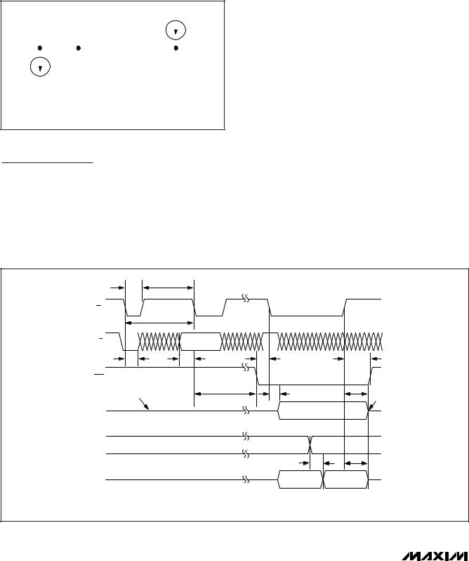
TIMING CHARACTERISTICS (Figures 1 and 2)
(AVDD = +4.75V to +5.25V, DVDD = +2.7V to AVDD, external reference = +4.096V, CREF = 4.7µF, CREFADJ = 0.1µF, CLOAD = 20pF, TA = TMIN to TMAX, unless otherwise noted. Typical values are at TA= +25°C.)
PARAMETER |
SYMBOL |
CONDITIONS |
MIN |
TYP |
MAX |
UNITS |
|
|
|
|
|
|
|
Acquisition Time |
tACQ |
|
1.1 |
|
|
µs |
Conversion Time |
tCONV |
|
|
|
4.7 |
|
|
|
|
|
|||
CS Pulse Width High |
tCSH |
(Note 6) |
40 |
|
|
ns |
CS Pulse Width Low (Note 6) |
tCSL |
VDVDD = 4.75V to 5.25V |
40 |
|
|
ns |
VDVDD = 2.7V to 5.25V |
60 |
|
|
|||
|
|
|
|
|
||
R/C to CS Fall Setup Time |
tDS |
|
0 |
|
|
ns |
R/C to CS Fall Hold Time |
tDH |
VDVDD = 4.75V to 5.25V |
40 |
|
|
ns |
VDVDD = 2.7V to 5.25V |
60 |
|
|
|||
|
|
|
|
|
||
CS to Output Data Valid |
tDO |
VDVDD = 4.75V to 5.25V |
|
|
40 |
ns |
VDVDD = 2.7V to 5.25V |
|
|
80 |
|||
|
|
|
|
|
||
HBEN Transition to Output Data |
tDO1 |
VDVDD = 4.75V to 5.25V |
|
|
40 |
ns |
Valid (MAX1166 Only) |
VDVDD = 2.7V to 5.25V |
|
|
80 |
||
|
|
|
|
|||
EOC Fall to CS Fall |
tDV |
|
0 |
|
|
ns |
|
|
|
|
|
|
|
4 _______________________________________________________________________________________
Low-Power, 16-Bit Analog-to-Digital Converter
with Parallel Interface
TIMING CHARACTERISTICS (Figures 1 and 2) (continued)
(AVDD = +4.75V to +5.25V, DVDD = +2.7V to AVDD, external reference = +4.096V, CREF = 4.7µF, CREFADJ = 0.1µF, CLOAD = 20pF, TA = TMIN to TMAX, unless otherwise noted. Typical values are at TA= +25°C.)
|
PARAMETER |
SYMBOL |
CONDITIONS |
MIN |
TYP |
MAX |
UNITS |
|
CS Rise to EOC Rise |
tEOC |
VDVDD = 4.75V to 5.25V |
|
|
40 |
ns |
|
VDVDD = 2.7V to 5.25V |
|
|
80 |
|||
|
|
|
|
|
|
||
|
Bus Relinquish Time (Note 6) |
tBR |
VDVDD = 4.75V to 5.25V |
|
|
40 |
ns |
|
VDVDD = 2.7V to 5.25V |
|
|
80 |
|||
|
|
|
|
|
|
||
|
|
|
|
|
|
|
|
Note 1: Relative accuracy is the deviation of the analog value at any code from its theoretical value after offset and gain errors have been removed.
Note 2: Offset nulled.
Note 3: Guaranteed by design, not production tested.
Note 4: Shutdown supply currents are typically 0.5µA, maximum specification is limited by automated test equipment. Note 5: Defined as the change in positive full scale caused by a ±5% variation in the nominal supply.
Note 6: To ensure best performance, finish reading the data and wait tBR before starting a new acquisition.
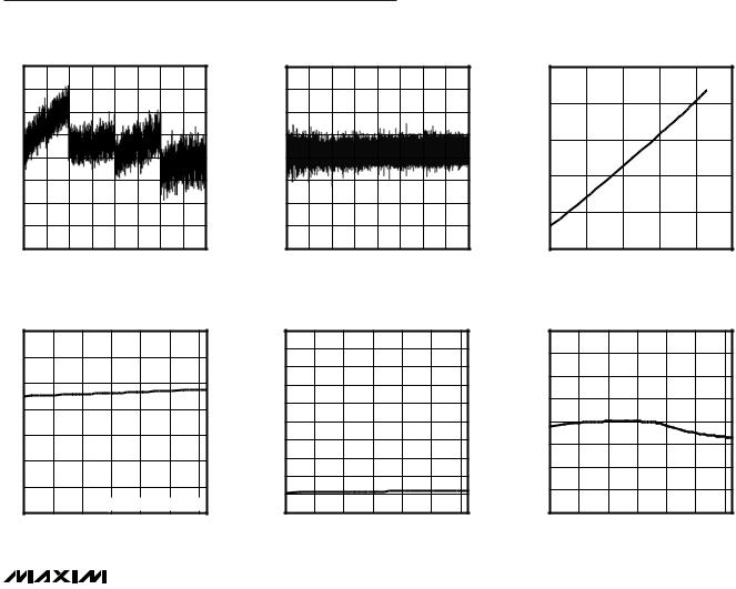
Typical Operating Characteristics
(AVDD = DVDD = +5V, external reference = +4.096V, CREF = 4.7µF, CREFADJ = 0.1µF, TA = +25°C, unless otherwise noted.)
INL vs. OUTPUT CODE |
DNL vs. OUTPUT CODE |
IAVDD + IDVDD SUPPLY CURRENT |
vs. SAMPLE RATE |
INL (LSB)
2.0
1.5
1.0
0.5
0
-0.5
-1.0
-1.5
-2.0
MAX1165/66 toc01
0 |
16384 |
32768 |
49152 |
65536 |
DNL (LSB)
2.0
1.5
1.0
0.5
0
-0.5
-1.0
-1.5
-2.0
MAX1165/66 toc02
0 |
16384 |
32768 |
49152 |
66536 |
|
10 |
|
|
|
|
toc03 |
|
|
|
|
|
|
|
(mA) |
1 |
|
|
|
|
MAX1165/66 |
|
|
|
|
|
||
CURRENT |
0.1 |
|
|
|
|
|
|
|
|
|
|
|
|
SUPPLY |
0.01 |
|
|
|
|
|
|
|
|
|
|
|
|
|
0.001 |
|
|
|
|
|
0.0001 |
|
|
|
|
|
|
|
0.01 |
0.1 |
1 |
10 |
100 |
1000 |
OUTPUT CODE |
OUTPUT CODE |
SAMPLE RATE (ksps) |
IAVDD + IDVDD SUPPLY CURRENT |
IAVDD + IDVDD SHUTDOWN CURRENT |
INTERNAL REFERENCE |
vs. TEMPERATURE |
vs. TEMPERATURE |
vs. TEMPERATURE |
|
3.5 |
|
|
|
|
|
toc04 |
5.0 |
|
|
|
|
|
toc05 |
|
4.136 |
|
|
|
|
|
toc06 |
|
|
|
|
|
|
|
4.5 |
|
|
|
|
|
|
|
|
|
|
|
|
|||
(mA)CURRENTSUPPLY |
3.0 |
|
|
|
|
|
MAX1165/66 |
|
|
|
|
|
MAX1165/66 |
(V)REFERENCEINTERNAL |
4.126 |
|
|
|
|
|
MAX1165/66 |
|
|
|
|
|
|
A)(CURRENTSHUTDOWN |
|
|
|
|
|
|
|
|
|
|
|||||||
|
|
|
|
|
|
|
|
|
|
|
|
|
|
|
|
|
|
|
|
|
||
|
|
|
|
|
|
|
4.0 |
|
|
|
|
|
|
|
|
|
|
|
|
|
|
|
|
|
|
|
|
|
|
|
|
|
|
|
|
|
|
4.116 |
|
|
|
|
|
|
|
|
2.5 |
|
|
|
|
|
|
3.5 |
|
|
|
|
|
|
|
|
|
|
|
|
|
|
|
|
|
|
|
|
|
|
|
|
|
|
|
|
|
|
|
|
|
|
|
||
|
2.0 |
|
|
|
|
|
|
3.0 |
|
|
|
|
|
|
|
4.106 |
|
|
|
|
|
|
|
|
|
|
|
|
|
|
|
|
|
|
|
|
|
|
|
|
|
|
|
||
|
|
|
|
|
|
|
2.5 |
|
|
|
|
|
|
|
4.096 |
|
|
|
|
|
|
|
|
|
|
|
|
|
|
|
|
|
|
|
|
|
|
|
|
|
|
|
|
||
|
1.5 |
|
|
|
|
|
|
2.0 |
|
|
|
|
|
|
|
4.086 |
|
|
|
|
|
|
|
|
|
|
|
|
|
|
|
|
|
|
|
|
|
|
|
|
|
|
|
||
|
|
|
|
|
|
|
|
|
|
|
|
|
|
|
|
|
|
|
|
|
|
|
|
1.0 |
|
|
|
|
|
|
1.5 |
|
|
|
|
|
|
|
4.076 |
|
|
|
|
|
|
|
|
|
|
|
|
|
|
|
|
|
|
|
|
|
|
|
|
|
|
|
||
|
|
|
|
|
|
|
|
1.0 |
|
|
|
|
|
|
|
|
|
|
|
|
|
|
|
0.5 |
|
|
|
|
|
|
|
|
|
|
|
|
|
|
|
|
|
|
|
|
|
|
|
|
|
|
|
|
0.5 |
|
|
|
|
|
|
|
4.066 |
|
|
|
|
|
|
|
|
|
|
|
SAMPLE RATE = 165ksps |
|
|
|
|
|
|
|
|
|
|
|
|
|
|
||||
|
0 |
|
|
0 |
|
|
|
|
|
|
|
4.056 |
|
|
|
|
|
|
||||
|
|
|
|
|
|
|
|
|
|
|
|
|
|
|
|
|
|
|
|
|||
|
-40 |
-20 |
0 |
20 |
40 |
60 |
80 |
-40 |
-20 |
0 |
20 |
40 |
60 |
80 |
|
-40 |
-20 |
0 |
20 |
40 |
60 |
80 |
|
|
|
TEMPERATURE (°C) |
|
|
|
|
TEMPERATURE (°C) |
|
|
|
|
|
TEMPERATURE (°C) |
|
|
||||||
MAX1165/MAX1166
_______________________________________________________________________________________ 5
MAX1165/MAX1166
Low-Power, 16-Bit Analog-to-Digital Converter with Parallel Interface
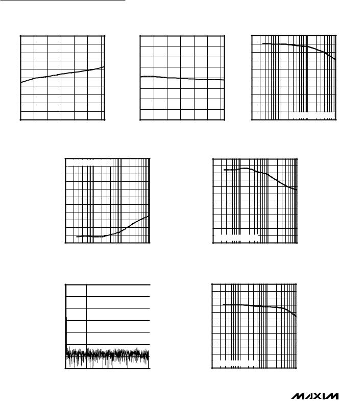
Typical Operating Characteristics (continued)
(AVDD = DVDD = +5V, external reference = +4.096V, CREF = 4.7µF, CREFADJ = 0.1µF, TA = +25°C, unless otherwise noted.)
OFFSET ERROR vs. TEMPERATURE
|
1000 |
|
|
|
|
|
toc07 |
|
800 |
|
|
|
|
|
|
|
|
|
|
|
|
MAX1165/66 |
|
|
600 |
|
|
|
|
|
|
V) |
400 |
|
|
|
|
|
|
( |
200 |
|
|
|
|
|
|
ERROR |
|
|
|
|
|
|
|
0 |
|
|
|
|
|
|
|
OFFSET |
-200 |
|
|
|
|
|
|
-400 |
|
|
|
|
|
|
|
|
|
|
|
|
|
|
|
|
-600 |
|
|
|
|
|
|
|
-800 |
|
|
|
|
|
|
|
-1000 |
|
|
|
|
|
|
|
-40 |
-20 |
0 |
20 |
40 |
60 |
80 |
|
|
|
TEMPERATURE (°C) |
|
|
||
GAIN ERROR |
SINAD vs. FREQUENCY |
vs. TEMPERATURE |
|
0.020 |
|
|
|
|
|
toc08 |
|
100 |
|
|
|
|
|
|
|
|
90 |
|
|
0.015 |
|
|
|
|
|
MAX1165/66 |
|
|
|
|
|
|
|
|
|
|
||
|
0.010 |
|
|
|
|
|
|
80 |
|
|
|
|
|
|
|
|
|
||
GAIN ERROR (%FSR) |
|
|
|
|
|
|
|
70 |
|
|
|
|
|
|
|
|
|
||
0.005 |
|
|
|
|
|
|
SINAD (dB) |
60 |
|
|
|
|
|
|
|
|
|||
0 |
|
|
|
|
|
|
50 |
||
-0.005 |
|
|
|
|
|
|
40 |
||
|
|
|
|
|
|
|
|||
|
|
|
|
|
|
|
30 |
||
|
-0.010 |
|
|
|
|
|
|
|
|
|
|
|
|
|
|
|
|
20 |
|
|
|
|
|
|
|
|
|
|
|
|
-0.015 |
|
|
|
|
|
|
|
10 |
|
|
|
|
|
|
|
|
|
|
|
-0.020 |
|
|
|
|
|
|
|
0 |
|
-40 |
-20 |
0 |
20 |
40 |
60 |
80 |
|
|
TEMPERATURE (°C)
MAX1165/66 toc09 |
SAMPLE RATE = 165ksps
0.1 |
1 |
10 |
100 |
|
FREQUENCY (kHz) |
|
|
THD vs. FREQUENCY |
SFDR vs. FREQUENCY |
THD (dB)
0
SAMPLE RATE = 165ksps
-10 -20 -30 -40 -50 -60 -70 -80 -90
-100 -110
0.1 |
1 |
10 |
|
FREQUENCY (kHz) |
|
MAX1165/66 toc10
100
SFDR (dB)
120
110
100
90
80
70
60
50
40
30
20
10
0
MAX1165/66 toc11 |
SAMPLE RATE = 165ksps |
0.1 |
1 |
10 |
100 |
|
FREQUENCY (kHz) |
|
|
FFT AT 1kHz |
SNR vs. FREQUENCY |
MAGNITUDE (dB)
0
-20
-40
-60
-80
-100
-120
-140
0
|
|
|
toc12 |
|
SAMPLE RATE = 165ksps |
||||
MAX1165/66 |
||||
|
|
|
||
|
|
|
|
|
20 |
40 |
60 |
80 |
|
FREQUENCY (kHz) |
|
|
SNR (dB)
120
110
100
90
80
70
60
50
40
30
20
10
0
MAX1165/66 toc13 |
SAMPLE RATE = 165ksps |
0.1 |
1 |
10 |
100 |
|
FREQUENCY (kHz) |
|
|
6 _______________________________________________________________________________________

Low-Power, 16-Bit Analog-to-Digital Converter
with Parallel Interface
Pin Description
PIN |
NAME |
FUNCTION |
|||
|
|
|
|
||
MAX1165 |
MAX1166 |
MAX1165 |
MAX1166 |
||
|
|||||
|
|
|
|
|
|
1 |
1 |
D8 |
D4/D12 |
Three-State Digital Data Output |
|
|
|
|
|
|
|
2 |
2 |
D9 |
D5/D13 |
Three-State Digital Data Output |
|
|
|
|
|
|
|
3 |
3 |
D10 |
D6/D14 |
Three-State Digital Data Output |
|
4 |
4 |
D11 |
D7/D15 |
Three-State Digital Data Output. D15 is the MSB. |
|
|
|
|
|
|
|
5 |
— |
D12 |
— |
Three-State Digital Data Output |
|
6 |
— |
D13 |
— |
Three-State Digital Data Output |
|
|
|
|
|
|
|
7 |
— |
D14 |
— |
Three-State Digital Data Output |
|
|
|
|
|
|
|
8 |
— |
D15 |
— |
Three-State Digital Data Output (MSB) |
|
|
|
|
|
|
|
|
|
|
|
Read/Convert Input. Power up and put the MAX1165/MAX1166 in acquisition mode |
|
|
|
|
|
by holding R/C low during the first falling edge of CS. During the second falling |
|
|
|
|
|
edge of CS, the level on R/C determines whether the reference and reference |
|
9 |
5 |
R/C |
buffer power down or remain on after conversion. Set R/C high during the second |
||
|
|
|
|
falling edge of CS to power down the reference and buffer, or set R/C low to leave |
|
|
|
|
|
the reference and buffer powered up. Set R/C high during the third falling edge of |
|
|
|
|
|
CS to put valid data on the bus. |
|
|
|
|
|
|
|
10 |
6 |
EOC |
End of Conversion. EOC drives low when conversion is complete. |
||
11 |
7 |
AVDD |
Analog Supply Input. Bypass with a 0.1µF capacitor to AGND. |
||
12 |
8 |
AGND |
Analog Ground. Primary analog ground (star ground). |
||
|
|
|
|
|
|
13 |
9 |
AIN |
Analog Input |
||
|
|
|
|
|
|
14 |
10 |
AGND |
Analog Ground. Connect pin 14 to pin 12 (MAX1165). Connect pin 10 to pin 8 |
||
(MAX1166). |
|||||
|
|
|
|
||
|
|
|
|
|
|
15 |
11 |
REFADJ |
Reference Buffer Output. Bypass REFADJ with a 0.1µF capacitor to AGND for internal |
||
reference mode. Connect REFADJ to AVDD to select external reference mode. |
|||||
|
|
|
|
||
16 |
12 |
REF |
Reference Input/Output. Bypass REF with a 4.7µF capacitor to AGND for internal |
||
reference mode. External reference input when in external reference mode. |
|||||
|
|
|
|
||
|
|
|
|
|
|
17 |
— |
RESET |
Reset Input. Logic high resets the device. |
||
|
|
|
|
|
|
|
|
|
|
High-Byte Enable Input. Used to multiplex the 14-bit conversion result: |
|
— |
13 |
HBEN |
1: Most significant byte available on the data bus. |
||
|
|
|
|
0: Least significant byte available on the data bus. |
|
|
|
|
|
|
|
|
|
|
|
Convert Start. The first falling edge of CS powers up the device and enables |
|
18 |
14 |
CS |
acquire mode when R/C is low. The second falling edge of CS starts conversion. |
||
|
|
|
|
The third falling edge of CS loads the result onto the bus when R/C is high. |
|
|
|
|
|
|
|
19 |
15 |
DGND |
Digital Ground |
||
|
|
|
|
|
|
20 |
16 |
DVDD |
Digital Supply Voltage. Bypass with a 0.1µF capacitor to DGND. |
||
21 |
17 |
D0 |
D0/D8 |
Three-State Digital Data Output |
|
|
|
|
|
|
|
22 |
18 |
D1 |
D1/D9 |
Three-State Digital Data Output |
|
|
|
|
|
|
|
23 |
19 |
D2 |
D2/D10 |
Three-State Digital Data Output |
|
|
|
|
|
|
|
24 |
20 |
D3 |
D3/D11 |
Three-State Digital Data Output |
|
|
|
|
|
|
|
25 |
— |
D4 |
— |
Three-State Digital Data Output |
|
26 |
— |
D5 |
— |
Three-State Digital Data Output |
|
27 |
— |
D6 |
— |
Three-State Digital Data Output |
|
28 |
— |
D7 |
— |
Three-State Digital Data Output |
|
|
|
|
|
|
|
_______________________________________________________________________________________ 7
MAX1165/MAX1166
MAX1165/MAX1166
Low-Power, 16-Bit Analog-to-Digital Converter with Parallel Interface
|
|
|
|
|
|
|
|
|
|
|
|
|
|
|
|
|
|
DVDD |
||||||||
|
|
|
|
|
|
|
|
|
|
|
|
|
|
|
|
|
1mA |
|
|
|
|
|||||
D0–D15 |
|
|
|
|
|
|
|
|
|
|
D0–D15 |
|
|
|
|
|
||||||||||
|
|
|
|
|
|
|
|
|
|
|
CLOAD = 20pF |
|
|
|
|
|
||||||||||
1mA |
|
|
|
|
|
|
|
|
|
|
|
|
|
|
|
|
|
|
CLOAD = 20pF |
|||||||
|
|
|
|
|
|
|
|
|
|
|
|
|
|
|
|
|
|
|||||||||
|
|
|
|
|
|
|
|
|
|
|
|
|
|
|
|
|
|
|
|
|||||||
|
|
|
|
|
|
|
|
DGND |
|
|
|
|
|
|
|
|
DGND |
|||||||||
|
|
|
|
|
|
|
|
|
|
|
|
|
|
|
|
|
|
|||||||||
a) HIGH-Z TO VOH, VOL TO VOH, |
b) HIGH-Z TO VOL, VOH TO VOL, |
|||||||||||||||||||||||||
AND VOH TO HIGH-Z |
AND VOL TO HIGH-Z |
|||||||||||||||||||||||||
Figure 1. Load Circuits
Detailed Description
Converter Operation
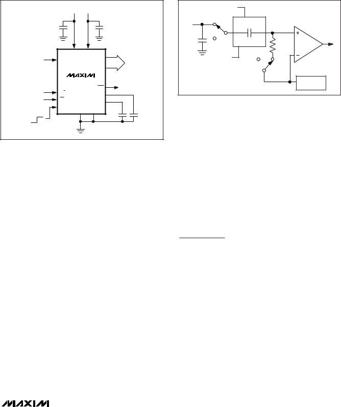
The MAX1165/MAX1166 use a successive-approxima- tion (SAR) conversion technique with an inherent track- and-hold (T/H) stage to convert an analog input into a 16-bit digital output. Parallel outputs provide a highspeed interface to most microprocessors (µPs). The Functional Diagram shows a simplified internal architecture of the MAX1165/MAX1166. Figure 3 shows a typical application circuit for the MAX1166.
Analog Input
The equivalent input circuit is shown in Figure 4. A switched capacitor digital-to-analog converter (DAC) provides an inherent T/H function. The single-ended input is connected between AIN and AGND.
Input Bandwidth
The ADC’s input-tracking circuitry has a 4MHz smallsignal bandwidth, so it is possible to digitize highspeed transient events and measure periodic signals with bandwidths exceeding the ADC’s sampling rate by using undersampling techniques. To avoid aliasing of unwanted high-frequency signals into the frequency band of interest, use anti-alias filtering.
Analog Input Protection
Internal protection diodes, which clamp the analog input to AVDD and/or AGND, allow the input to swing from AGND - 0.3V to AVDD + 0.3V, without damaging the device.
If the analog input exceeds 300mV beyond the supplies, limit the input current to 10mA.
|
tCSH |
|
|
tCSL |
|
CS |
|
|
|
tACQ |
|
R/C |
REF POWER- |
|
DOWN BIT |
||
|
tDH |
tDS |
tDV |
tEOC |
EOC |
|
|
|
HIGH-Z |
tCONV |
tDO |
tBR |
|
HIGH-Z |
||
|
|
||
|
|
|
|
D0–D15 |
|
DATA VALID |
|
HBEN* |
|
|
|
|
|
tDO1 |
tBR |
|
|
|
|
D8/D15– |
|
HIGH-/LOW- |
HIGH-/LOW- |
D0/D7* |
|
BYTE VALID |
BYTE VALID |
*HBEN AND BYTE-WIDE DATA BUS AVAILABLE ON MAX1166 ONLY.
Figure 2. MAX1165/MAX1166 Timing Diagram
8 _______________________________________________________________________________________
Low-Power, 16-Bit Analog-to-Digital Converter
with Parallel Interface
+5V ANALOG |
+5V DIGITAL |
0.1 F |
|
|
|
0.1 F |
|
|
|
AVDD |
DVDD |
P DATA |
|
||
|
BUS |
|
||||
ANALOG INPUT |
AIN |
|
D0–D7 |
|
|
|
|
OR |
|
|
|||
|
|
|
|
|
||
|
|
|
D8–D15 |
|
|
|
|
MAX1166 |
|
|
|||
|
R/C |
|
EOC |
|
|
|
|
|
REF |
|
|
||
|
CS |
|
|
|
||
|
|
REFADJ |
|
|
||
|
|
|
|
|
||
HIGH |
HBEN |
|
|
|
|
|
AGND |
DGND |
|
|
|||
BYTE |
0.1 F |
4.7 F |
||||
|
|
|
||||
LOW |
|
|
|
|
|
|
BYTE |
|
|
|
|
|
|
Figure 3. Typical Application Circuit for the MAX1166
Track and Hold (T/H)
In track mode, the analog signal is acquired on the internal hold capacitor. In hold mode, the T/H switches open and the capacitive DAC samples the analog input.
During the acquisition, the analog input (AIN) charges capacitor CDAC. The acquisition ends on the second falling edge of CS. At this instant, the T/H switches open. The retained charge on CDAC represents a sample of the input.
In hold mode, the capacitive DAC adjusts during the remainder of the conversion time to restore node ZERO to zero within the limits of 16-bit resolution. Force CS low to put valid data on the bus at the end of the conversion.
The time required for the T/H to acquire an input signal is a function of how quickly its input capacitance is charged. If the input signal’s source impedance is high, the acquisition time lengthens and more time must be allowed between conversions. The acquisition time (tACQ) is the maximum time the device takes to acquire the signal. Use the following formula to calculate acquisition time:
tACQ = 11 (RS + RIN) 35pF
where RIN = 800Ω, RS = the input signal’s source impedance, and tACQ is never less than 1.1µs. A source impedance less than 1kΩ does not significantly affect the ADC’s performance.
To improve the input signal bandwidth under AC conditions, drive AIN with a wideband buffer (>4MHz) that can drive the ADC’s input capacitance and settle quickly.
|
REF |
|
|
|
TRACK |
CAPACITIVE DAC |
|
AIN |
|
|
|
|
|
ZERO |
|
|
|
|
|
CSWITCH |
|
CDAC = 32pF |
RIN |
3pF |
HOLD |
||
|
|
|
800Ω |
|
AGND |
HOLD |
TRACK |
|
|
|
AUTOZERO |
|
|
|
RAIL |
Figure 4. Equivalent Input Circuit
Power-Down Modes
Select standby mode or shutdown mode with the R/C bit during the second falling edge of CS (see the
Selecting Standby or Shutdown Mode section). The MAX1165/MAX1166 automatically enter either standby mode (reference and buffer on) or shutdown (reference and buffer off) after each conversion depending on the status of R/C during the second falling edge of CS.
Internal Clock
The MAX1165/MAX1166 generate an internal conversion clock. This frees the microprocessor from the burden of running the SAR conversion clock. Total conversion time after entering hold mode (second falling edge of CS) to end of conversion (EOC) falling is 4.7µs (max).
Applications Information
Starting a Conversion
CS and R/C control acquisition and conversion in the MAX1165/MAX1166 (Figure 2). The first falling edge of CS powers up the device and puts it in acquire mode if R/C is low. The convert start is ignored if R/C is high. The MAX1165/MAX1166 need at least 10ms (CREFADJ = 0.1µF, CREF = 4.7µF) for the internal reference to wake up and settle before starting the conversion if powering up from shutdown. The ADC can wake up, from shutdown, to an unknown state. Put the ADC in a known state by completing one “dummy” conversion. The MAX1165/MAX1166 are in a known state, ready for actual data acquisition, after the completion of the dummy conversion. A dummy conversion consists of one full conversion cycle.
The MAX1165 provides an alternative reset function to reset the device (see the RESET section).
MAX1165/MAX1166
_______________________________________________________________________________________ 9
Low-Power, 16-Bit Analog-to-Digital Converter with Parallel Interface
MAX1165/MAX1166 |
|
|
CONVERSION |
DATA |
|
|
ACQUISITION |
OUT |
|||
CS |
REF POWER- |
|
|
||
|
DOWN BIT |
|
|
||
R/C |
|
|
|
||
EOC |
|
|
|
||
REF |
|
|
|
||
AND |
|
|
|
||
BUFFER |
|
|
|
||
Figure 5. Selecting Standby Mode |
|
||||
|
Selecting Standby or Shutdown Mode |
||||
The MAX1165/MAX1166 have a selectable standby or |
|||||
|
|||||
|
low-power shutdown mode. In standby mode, the |
||||
|
ADC’s internal reference and reference buffer do not |
||||
|
power down between conversions, eliminating the need |
||||
|
to wait for the reference to power up before performing |
||||
|
the next conversion. Shutdown mode powers down the |
||||
|
reference and reference buffer after completing a con- |
||||
|
version. The reference and reference buffer require a |
||||
|
minimum of 10ms (CREFADJ = 0.1µF, CREF = 4.7µF) to |
||||
|
power up and settle from shutdown. |
|
|||
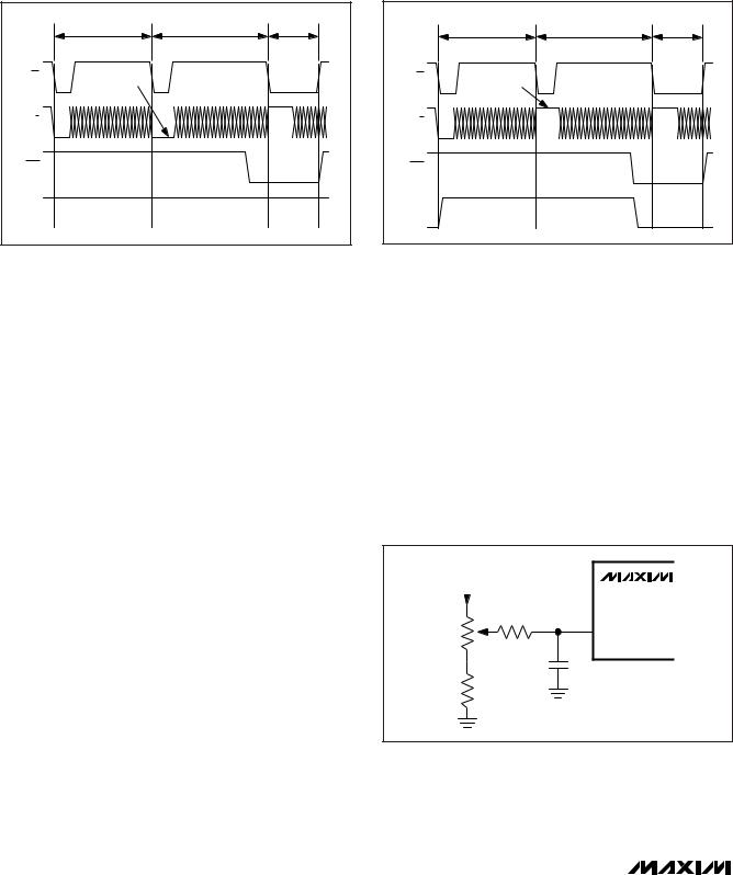
The state of R/C at the second falling edge of CS selects which power-down mode the MAX1165/ MAX1166 enter upon conversion completion. Holding R/C low causes the MAX1165/MAX1166 to enter standby mode. The reference and buffer are left on after the conversion completes. R/C high causes the MAX1165/ MAX1166 to enter shutdown mode and shut down the reference and buffer after conversion (Figures 5 and 6). When using an external reference, set the REF powerdown bit high for lowest current operation.
Standby Mode
While in standby mode, the supply current is reduced to less than 1mA (typ). The next falling edge of CS with R/C low causes the MAX1165/MAX1166 to exit standby mode and begin acquisition. The reference and reference buffer remain active to allow quick turn-on time. Standby mode allows significant power savings while running at the maximum sample rate.
Shutdown Mode
In shutdown mode, the reference and reference buffer are shut down between conversions. Shutdown mode reduces supply current to 0.5µA (typ) immediately after the conversion. The falling edge of CS with R/C low
|
|
CONVERSION |
DATA |
|
ACQUISITION |
OUT |
|
CS |
REF POWER- |
|
|
|
DOWN BIT |
|
|
R/C |
|
|
|
EOC |
|
|
|
REF |
|
|
|
AND |
|
|
|
BUFFER |
|
|
|
Figure 6. Selecting Shutdown Mode
causes the reference and buffer to wake up and enter acquisition mode. To achieve 16-bit accuracy, allow 10ms (CREFADJ = 0.1µF, CREF = 4.7µF) for the internal reference to wake up.
Internal and External Reference
Internal Reference
The internal reference of the MAX1165/MAX1166 is internally buffered to provide +4.096V output at REF. Bypass REF to AGND and REFADJ to AGND with 4.7µF and 0.1µF, respectively.
Fine adjustments can be made to the internal reference voltage by sinking or sourcing current at REFADJ. The input impedance of REFADJ is nominally 5kΩ. The internal reference voltage is adjustable to ±1.5% with the circuit of Figure 7.
|
+5V |
MAX1165 |
|
|
|
|
|
MAX1166 |
|
|
68kΩ |
100kΩ |
|
REFADJ |
0.1 F
150kΩ
Figure 7. MAX1165/MAX1166 Reference Adjust Circuit
External Reference
An external reference can be placed at either the input (REFADJ) or the output (REF) of the MAX1165/ MAX1166s’ internal buffer amplifier. When connecting an
10 ______________________________________________________________________________________