

бакМИТ_КП2015 / Компоненты по вариантам / АЦП / MAX194
.pdf14-Bit, 85ksps ADC with 10µA Shutdown
MAX194
Figure 21. MAX194 Code Listing for 68HC16 Module and Circuit of Figure 19 (continued)
Constraints on sequencing the four power supplies are as follows.
•Apply VDDA before VDDD.
•Apply VSSA before VSSD.
•Apply AIN and REF after VDDA and VSSA are present.
•The power supplies should settle within the
MAX194’s power-on delay (minimum 500ns) or you should recalibrate the converter (pulse RESET low) before use.
Be sure that digital return currents do not pass through the analog ground and that return-current paths are low impedance. A 5mA current flowing through a PC board ground trace impedance of only 0.1Ω creates an error voltage of about 500µV, or about 1LSB error with a ±4V full-scale system.
The board layout should ensure as much as possible that digital and analog signal lines are kept separate. Do not run analog and digital (especially clock) lines parallel to one another. If you must cross one with the other, do so at right angles.
The ADC’s high-speed comparator is sensitive to highfrequency noise on the VDDA and VSSA power supplies. Bypass these supplies to the analog ground plane with 0.1µF in parallel with 1µF or 10µF low-ESR capacitors. Keep capacitor leads short for best supplynoise rejection.
Shutdown
The MAX194 may be shut down by pulling BP/UP/ SHDN low. In addition to lowering power dissipation to 10µW (100µW max) when the device is not in use, considerable power savings is possible by shutting the converter down for short periods between conversions. There is no need to perform a reset (calibration) after the converter has been shut down unless the time in shutdown is long enough that the supply voltages or ambient temperature may have changed.
The time required for the converter to “wake up” and settle depends heavily on the amount of additional error acceptable. For 0.1LSB additional error, 3.2µs is sufficient settling time and also allows enough time for reacquisition of the analog input signal. 20µs settling is required for less than 0.05LSB error. Figure 23 is a
______________________________________________________________________________________ 21
14-Bit, 85ksps ADC with 10µA Shutdown
MAX194 |
10Ω |
|
|
|
(mW)DISSIPATION |
|
|
|
|
|
|
|
|
|
VDDD |
|
|
|
10μF |
|
VDDA |
|
|
|
|
|
|
|
|
|
5V |
|
0.1μF |
|
|
|
|
|
MAX194 |
|
|
|
10μF |
0.1μF |
|
|
|
|
|
|
|
||
|
|
|
DGND |
|
|
|
|
|
AGND |
|
POWER |
|
10μF |
|
|
|
|
|
|
|
|
|
|
|
5V |
|
0.1μF |
|
|
|
|
0.1μF |
|
|
|
|
10μF |
|
|
|
|
|
|
|
|
|
|
|
|
|
VSSA |
|
|
|
|
|
VSSD |
|
|
|
10Ω |
|
|
|
|
100
10
1
0.1
0.01
MAX194-FIG23
20μs WAKE-UP DELAY
0.05LSB ERROR
3.2μs WAKE-UP DELAY 0.1LSB ERROR
1 |
10 |
100 |
1000 |
10,000 |
100,000 |
CONVERSIONS PER SECOND
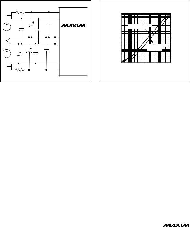
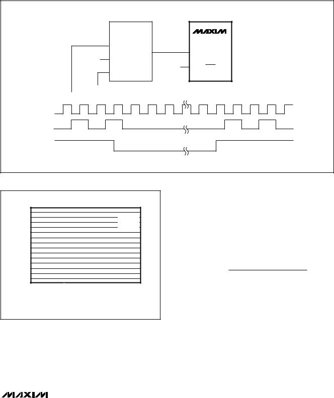
Figure 22. Supply Bypassing and Grounding |
Figure 23. Power Dissipation vs. Conversions/sec When |
|
Shutting the MAX194 Down Between Conversions |
graph of theoretical power consumption vs. conversions per second for the MAX194 that assumes the conversion clock is 1.7MHz and the converter is shut down as much as possible between conversions.
Stop CLK before shutting down the MAX194. CLK must be stopped without generating short clock pulses. Short CLK pulses (less than 150ns), or shutting down the MAX194 without stopping CLK, may adversely affect the MAX194’s internal calibration data. In applications where CLK is free-running and asynchronous, use the circuit of Figure 24 to stop CLK cleanly.
To minimize the time required to settle and perform a conversion, shut the converter down only after a conversion is finished and the desired mode (unipolar or bipolar) has been set. This ensures that the sampling capacitor array is properly connected to the input signal. If shut down in mid-conversion, when awakened, the MAX194 finishes the old conversion, allows four clock (CLK) cycles for input acquisition, then begins the new conversion.
_____________Dynamic Performance
High-speed sampling capability, 85ksps throughput, and wide dynamic range make the MAX194 ideal for AC applications and signal processing. To support these and other related applications, Fast Fourier Transform (FFT) test techniques are used to guarantee the ADC’s dynamic frequency response, distortion, and noise at the rated throughput. Specifically, this involves
applying a low-distortion sine wave to the ADC input and recording the digital conversion results for a specified time. The data is then analyzed using an FFT algorithm, which determines its spectral content. Conversion errors are then seen as spectral elements other than the fundamental input frequency.
Signal-to-Noise Ratio and
Effective Number of Bits
Signal-to-Noise Ratio (SNR) is the ratio between the RMS amplitude of the fundamental input frequency to the RMS amplitude of all other ADC output signals. The output band is limited to frequencies above DC and below one-half the ADC sample rate. This usually (but not always) includes distortion as well as noise components. For this reason, the ratio is sometimes referred to as Signal-to-Noise + Distortion (SINAD).
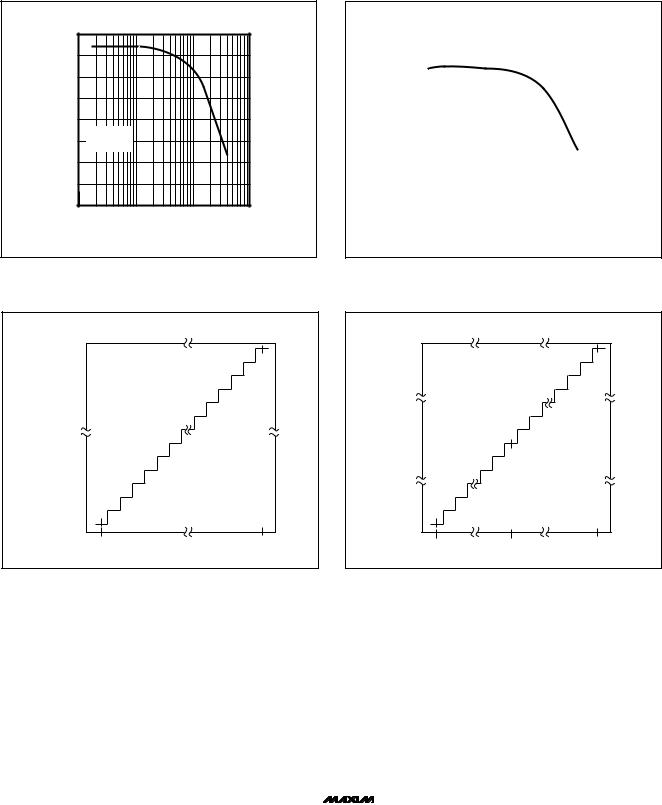
The theoretical minimum ADC noise is caused by quantization error and is a direct result of the ADC’s resolution: SNR = (6.02N + 1.76)dB, where N is the number of bits of resolution. A perfect 14-bit ADC can, therefore, do no better than 86dB. An FFT plot of the output shows the output level in various spectral bands. Figure 25 shows the result of sampling a pure 1kHz sinusoid at 85ksps with the MAX194.
By transposing the equation that converts resolution to SNR, we can, from the measured SNR, determine the effective resolution or the “effective number of bits” the ADC provides: N = (SNR - 1.76) / 6.02. Substituting SINAD for SNR in this formula results in a better
22 ______________________________________________________________________________________
14-Bit, 85ksps ADC with 10µA Shutdown
|
1/2 |
74HC73 |
MAX194 |
|
|
|
|
|
J |
|
CLK |
|
|
Q |
|
|
K |
|
|
+5V |
|
|
|
|
|
|
BP/UP/SHDN |
CK
2 x CLK
CLOCK SHUTDOWN
CK (2 x CLK)
Q (CLK)
J (CLOCK SHUTDOWN)
MAX194
Figure 24. Circuit to Stop Free-Running Asynchronous CLK
fIN = 1kHz fS = 85kHz TA = +25°C
Figure 25. MAX194 FFT Plot
measure of the ADC’s usefulness. Figure 26 shows the effective number of bits as a function of the MAX194’s input frequency calculated from the SINAD.
Total Harmonic Distortion
If a pure sine wave is input to an ADC, AC integral nonlinearity (INL) of an ADC’s transfer function results in harmonics of the input frequency being present in the sampled output data.
Total Harmonic Distortion (THD) is the ratio of the RMS sum of all the harmonics (in the frequency band above DC and below one-half the sample rate, but not including the DC component) to the RMS amplitude of the fundamental frequency. This is expressed as follows:
√(V22 + V32 + V42 + ... + VN2) THD = 20log——————————————
V1
where V1 is the fundamental RMS amplitude, and V2 through VN are the amplitudes of the 2nd through Nth harmonics. The THD specification in the Electrical Characteristics includes the 2nd through 5th harmonics. In the MAX194, this distortion is caused primarily by the changes in on-resistance of the AIN sampling switches with changing input voltage. These resistance changes, together with the DAC’s capacitance (which can also vary with input voltage), cause a varying time delay for AC signals, which causes significant distortion at moderately high frequencies (Figure 27).
______________________________________________________________________________________ 23
14-Bit, 85ksps ADC with 10µA Shutdown
MAX194 |
BITSEFFECTIVE |
11.5 |
|
|
MAX194-26 |
(dB)SINAD |
|
|
14.0 |
|
|
|
|
|
|
13.5 |
|
|
|
|
|
|
13.0 |
|
|
|
|
|
|
12.5 |
|
|
|
|
|
|
12.0 |
|
|
|
|
|
|
|
fS = 85kHz |
|
|
|
|
|
|
TA = +25°C |
|
|
|
|
|
11.0 |
|
|
|
|
|
|
10.5 |
|
|
|
|
|
|
10.0 |
|
|
|
|
|
|
0.1 |
1 |
10 |
100 |
|
|
|
|
INPUT FREQUENCY (kHz) |
|
|
|
90 |
|
|
|
|
|
|
|
|
|
|
|
|
|
|
|
|
|
|
|
|
|
|
|
|
|
|
-27 |
|
|
|
|
|
|
|
|
|
|
|
|
|
|
|
|
|
|
|
|
|
|
|
|
|
|
||
|
|
fS = 85kHz |
|
|
|
|
|
|
|
|
|
|
|
|
|
|
|
|
|
MAX194 |
|||||||
85 |
|
TA = +25°C |
|
|
|
|
|
|
|
|
|
|
|
|
|
|
|
|
|
||||||||
|
|
|
|
|
|
|
|
|
|
|
|
|
|
|
|
|
|
|
|||||||||
|
|
|
|
|
|
|
|
|
|
|
|
|
|
|
|
|
|
|
|
|
|
|
|
|
|
|
|
80 |
|
|
|
|
|
|
|
|
|
|
|
|
|
|
|
|
|
|
|
|
|
|
|
|
|
|
|
|
|
|
|
|
|
|
|
|
|
|
|
|
|
|
|
|
|
|
|
|
|
|
|
|
|
|
|
75 |
|
|
|
|
|
|
|
|
|
|
|
|
|
|
|
|
|
|
|
|
|
|
|
|
|
|
|
|
|
|
|
|
|
|
|
|
|
|
|
|
|
|
|
|
|
|
|
|
|
|
|
|
|
|
|
70 |
|
|
|
|
|
|
|
|
|
|
|
|
|
|
|
|
|
|
|
|
|
|
|
|
|
|
|
|
|
|
|
|
|
|
|
|
|
|
|
|
|
|
|
|
|
|
|
|
|
|
|
|
|
|
|
65 |
|
|
|
|
|
|
|
|
|
|
|
|
|
|
|
|
|
|
|
|
|
|
|
|
|
|
|
|
|
|
|
|
|
|
|
|
|
|
|
|
|
|
|
|
|
|
|
|
|
|
|
|
|
|
|
60 |
|
|
|
|
|
|
|
|
|
|
|
|
|
|
|
|
|
|
|
|
|
|
|
|
|
|
|
|
|
|
|
|
|
|
|
|
|
|
|
|
|
|
|
|
|
|
|
|
|
|
|
|
|
|
|
0.1 |
1 |
|
10 |
|
100 |
||||||||||||||||||||||
FREQUENCY (kHz)
Figure 26. Effective Bits vs. Input Frequency |
Figure 27. Signal-to-Noise + Distortion vs. Frequency |
11 . . . 111
11 . . . 110
11 . . . 101
11 . . . 100
11 . . . 011
11 . . . 010
00 . . . 110
00 . . . 101
00 . . . 100
00 . . . 011
00 . . . 010
00 . . . 001
00 . . . 000
0V |
VREF - (1LSB) |
11 . . . 111
11 . . . 110
11 . . . 101
10 . . . 010
10 . . . 001
10 . . . 000
01 . . . 111
01 . . . 110
00 . . . 010
00 . . . 001
00 . . . 000
-VREF |
0V |
VREF - (1LSB) |
Figure 28. MAX194 Unipolar Transfer Function |
Figure 29. MAX194 Bipolar Transfer Function |
Spurious-Free Dynamic Range
Spurious-free dynamic range is the ratio of the fundamental RMS amplitude to the amplitude of the next largest spectral component (in the frequency band above DC and below one-half the sample rate). Usually, this peak occurs at some harmonic of the input frequency. However, if the ADC is exceptionally linear, it may occur only at a random peak in the ADC’s noise floor.
Transfer Function
Figures 28 and 29 show the MAX194’s transfer functions. In unipolar mode, the output data is in binary format and in bipolar mode it is offset binary.
TRANSISTOR COUNT: 7966
Maxim cannot assume responsibility for use of any circuitry other than circuitry entirely embodied in a Maxim product. No circuit patent licenses are implied. Maxim reserves the right to change the circuitry and specifications without notice at any time.
24 ____________________Maxim Integrated Products, 120 San Gabriel Drive, Sunnyvale, CA 94086 408-737-7600
© 1997 Maxim Integrated Products |
Printed USA |
is a registered trademark of Maxim Integrated Products. |