

ADS8339
SBAS677A –JUNE 2014–REVISED OCTOBER 2014 |
www.ti.com |
12 Layout
12.1 Layout Guidelines
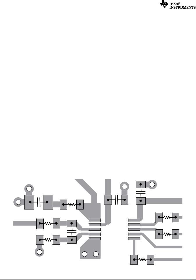
Figure 64 shows one of the board layouts as an example when using ADS8339 in a circuit.
•A printed circuit board (PCB) board with at least four layers is recommended to keep all critical components on the top layer.
•Analog input signals and the reference input signals must be kept away from noise sources. Crossing digital lines with the analog signal path should be avoided. The analog input and the reference signals are routed on to the left side of the board and the digital connections are routed on the right side of the device.
•Due to the dynamic currents that occur during conversion and data transfer, each supply pin (AVDD and DVDD) must have a decoupling capacitor that keeps the supply voltage stable. TI recommends using one 1- μF ceramic capacitor at each supply pin.
•A layout that interconnects the converter and accompanying capacitors with the low inductance path is critical for achieving optimal performance. Using 15-mil vias to interconnect components to a solid analog ground plane at the subsequent inner layer minimizes stray inductance. Avoid placing vias between the supply pin and the decoupling capacitor. Any inductance between the supply capacitor and the supply pin of the converter must be kept to less than 5 nH by placing the capacitor within 0.2 inches from the supply or input pins of the ADS8339 and by using 20-mil traces, as shown in Figure 64.
•Dynamic currents are also present at the REFIN pin during the conversion phase. Therefore, good decoupling is critical to achieve optimal performance. The inductance between the reference capacitor and the REFIN pin must be kept to less than 2 nH by placing the capacitor within 0.1 inches from the REFIN pin and by using 20-mil traces.
•A single 10-μF, X7R-grade, 0805-size ceramic capacitor with at least a 10-V rating is recommended for good performance over temperature range.
•A small, 0.1-Ω to 0.47-Ω, 0603-size resistor placed in series with the reference capacitor keeps the overall impedance low and constant, especially at very high frequencies.
•Avoid using additional lower value capacitors because the interactions between multiple capacitors can affect the ADC performance at higher sampling rates.
•Place the RC filters immediately next to the input pins. Among surface-mount capacitors, COG (NPO) ceramic capacitors provide the best capacitance precision. The type of dielectric used in COG (NPO) ceramic capacitors provides the most stable electrical properties over voltage, frequency, and temperature changes.
12.2 Layout Example
|
REF |
|
10PF |
GND |
0.1O t 0.47O |
|
REF |
|
1: REF |
Analog Input |
2: AVDD |
|
|
|
3: AINP |
|
4: AINN |
|
GND |
|
5: GND |
GND
AVDD |
|
GND |
|
|
|
|
1PF |
1PF |
|
|
GND |
AVDD |
|
DVDD |
|
|
10: DVDD |
9: SDI
8: SCLK
7: SDO
6: CONVST
DVDD
47O
47O
SDO
47O
Figure 64. Board Layout Example
32 |
Submit Documentation Feedback |
Copyright © 2014, Texas Instruments Incorporated |
Product Folder Links: ADS8339