

TMS320C6727B, TMS320C6726B, TMS320C6722B, TMS320C6720
Floating-Point Digital Signal Processors
www.ti.com
SPRS370C–SEPTEMBER 2006–REVISED OCTOBER 2007
2.5 Program Cache
The C672x DSP executes code directly from a large on-chip 32K-byte program cache. The program cache has these key features:
∙Wide 256-bit path to internal ROM/RAM
∙Single-cycle access on cache hits
∙2-cycle miss penalty to internal ROM/RAM
∙Caches external memory as well as ROM/RAM
∙Direct-mapped
∙Modes: Enable, Freeze, Bypass
∙Software invalidate to support code overlay
The program cache line size is 256 bits wide and is matched with a 256-bit-wide path between cache and internal memory. This allows the program cache to fill an entire line (corresponding to eight C67x+ CPU instructions) with only a single miss penalty of 2 cycles.
The program cache control registers are listed in Table 2-4.
Table 2-4. Program Cache Control Registers
REGISTER NAME |
BYTE ADDRESS |
DESCRIPTION |
L1PISAR |
0x2000 0000 |
L1P Invalidate Start Address |
L1PICR |
0x2000 0004 |
L1P Invalidate Control Register |
CAUTION
Any application which modifies the contents of program RAM (for example, a program overlay) must invalidate the addresses from program cache to maintain coherency by explicitly writing to the L1PISAR and L1PICR registers.
The Cache Mode (Enable, Freeze, Bypass) is configured through a CPU internal register (CSR, bits 7:5). These options are listed in Table 2-5. Typically, only the Cache Enable Mode is used. But advanced users may utilize Freeze and Bypass modes to tune performance.
Table 2-5. Cache Modes Set Through PCC Field of CSR CPU Register on C672x
CPU CSR[7:5] |
CACHE MODE |
000b |
Enable (Deprecated - Means direct mapped RAM on some C6000 devices) |
010b |
Enable - Cache is enabled, cache misses cause a line fill. |
011b |
Freeze - Cache is enabled, but contents are unchanged by misses. |
100b |
Bypass - Forces cache misses, cache contents frozen. |
Other Values |
Reserved - Not Supported |
CAUTION
Although the reset value of CSR[7:5] (PCC field) is 000b, the value may be modified during the boot process by the ROM code. Refer to the appropriate ROM data sheet for more details. However, note that the cache may be disabled when control is actually passed to application code. Therefore, it may be necessary to write '010b' to the PCC field to explicitly enable the cache at the start of application code.
CAUTION
Changing the cache mode through CSR[7:5] does not invalidate any lines already in the cache. To invalidate the cache after modifications are made to program space, the control registers L1PISAR and L1PICR must be used.
Submit Documentation Feedback |
Device Overview |
11 |
TMS320C6727B, TMS320C6726B, TMS320C6722B, TMS320C6720
Floating-Point Digital Signal Processors
www.ti.com
SPRS370C–SEPTEMBER 2006–REVISED OCTOBER 2007
2.6 High-Performance Crossbar Switch
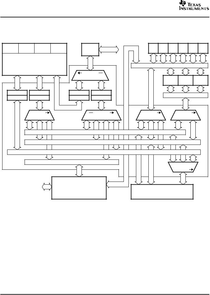
The C672x DSP includes a high-performance crossbar switch that acts as a central hub between bus masters and targets. Figure 2-4 illustrates the connectivity of the crossbar switch.
ROM |
RAM |
CPU |
Program |
|
|
|
|
|
PLL |
RTI |
SPI0 |
SPI1 |
I2C0 |
I2C1 |
|||
Cache |
|
EMIF |
|
|
|
|
|||||||||||
|
|
|
|
|
|
|
|
|
|
|
|
|
|
|
|
||
|
Memory Controller |
|
|
|
External |
|
|
|
|
|
|
|
|
|
|||
|
T2 |
|
|
Memory |
|
|
|
|
|
|
|
|
|
||||
Data |
|
|
CPU |
Program |
|
|
|
SDRAM/ |
|
|
|
|
|
|
|
|
|
|
|
|
|
|
Flash |
|
|
|
|
|
|
|
|
|
|||
Master |
|
Slave |
Master |
|
|
|
|
|
Peripheral Configuration Bus |
|
|
|
|||||
|
|
|
|
|
|
|
|
|
|
||||||||
Port |
|
|
Port |
Port |
|
|
|
|
|
T3 |
|
|
|
|
|
|
|
(DMP) |
|
|
(CSP) |
(PMP) |
Priority |
|
|
|
|
|
|
|
|
||||
|
|
|
|
|
|
|
|
|
|
|
|
||||||
M1 |
|
T1 |
M2 |
2 |
|
1 |
|
|
|
|
McASP0 |
McASP1 |
McASP2 |
||||
|
|
|
|
|
|
|
|
|
|
|
|
||||||
BR1 |
|
BR2 |
|
BR3 |
BR4 |
|
|
|
|
|
|
|
|
|
|
||
SYSCLK1 |
|
SYSCLK1 |
|
SYSCLK3 |
|
SYSCLK3 |
|
|
|
|
McASP DMA Bus |
|
|||||
SYSCLK2 |
|
SYSCLK2 |
|
SYSCLK1 |
|
SYSCLK2 |
|
|
|
|
|
||||||
|
|
|
|
|
|
|
|
|
|
|
|
||||||
|
|
|
|
|
|
|
|
|
|
|
|
|
T4 |
|
|
|
|
|
|
|
Priority |
|
|
|
Priority |
|
|
Priority |
|
|
Priority |
|
|
|
|
|
|
1 |
2 |
3 |
1 |
2 |
3 |
4 |
1 |
2 |
3 |
|
1 |
|
2 |
|
|
|
|
|
|
|
dMAX MAX0 Unit Master Port − High Priority |
|
|
|
|
|
|
|
|
||||
|
|
|
|
|
dMAX MAX1 Unit Master Port − Second Priority |
|
|
|
|
|
|
|
|
||||
|
|
|
|
|
Memory Controller DMP − Data Read/W rite by CPU |
|
|
|
|
|
|
|
|||||
|
|
|
UHPI Master Interface (External Host CPU) |
|
|
|
|
|
1 |
2 |
|
3 |
|
||||
Crossbar |
|
|
|
|
|
|
|
|
|
|
|
|
|
|
|||
|
|
|
|
|
|
|
|
|
|
|
|
Priority |
|
|
|
||
|
|
|
|
|
|
|
|
|
|
|
|
|
|
|
|
||
|
|
|
|
|
M5 |
|
|
|
|
|
|
|
|
|
|
|
|
|
|
External |
|
UHPI |
|
Config |
M3 |
|
M4 |
T5 |
|
|
|
||||
|
|
|
|
|
|
|
|
|
|
|
|
|
|||||
|
|
Host MCU |
|
Universal Host-Port |
|
|
|
MAX0 |
MAX1 |
|
|
Config |
|
|
|
||
|
|
|
|
|
Interface |
|
|
|
|
|
|
dMAX |
|
|
|
|
|
Figure 2-4. Block Diagram of Crossbar Switch
As shown in Figure 2-4, there are five bus masters:
M1 |
Memory controller DMP for CPU data accesses to peripherals and EMIF. |
M2 |
Memory controller PMP for program cache fills from the EMIF. |
M3 |
dMAX HiMAX master port for high-priority DMA accesses. |
M4 |
dMAX LoMAX master port for lower-priority DMA accesses. |
M5 |
UHPI master port for an external MCU to access on-chip and off-chip memories. |
12 |
Device Overview |
Submit Documentation Feedback |

TMS320C6727B, TMS320C6726B, TMS320C6722B, TMS320C6720
Floating-Point Digital Signal Processors
www.ti.com
SPRS370C–SEPTEMBER 2006–REVISED OCTOBER 2007
The five bus masters arbitrate for five different target groups:
T1 |
On-chip memories through the CPU Slave Port (CSP). |
T2 |
Memories on the external memory interface (EMIF). |
T3 |
Peripheral registers through the peripheral configuration bus. |
T4 |
McASP serializers through the dedicated McASP DMA bus. |
T5 |
dMAX registers. |
The crossbar switch supports parallel accesses from different bus masters to different targets. When two or more bus masters contend for the same target beginning at the same cycle, then the highest-priority master is given ownership of the target while the other master(s) are stalled. However, once ownership of the target is given to a bus master, it is allowed to complete its access before ownership is arbitrated again. Following are two examples.
Example 1: Simultaneous accesses without conflict
∙dMAX HiMAX accesses McASP Data Port for transfer of audio data.
∙dMAX LoMAX accesses SPI port for control processing.
∙UHPI accesses internal RAM through the CSP.
∙CPU fills program cache from EMIF.
Example 2: Conflict over a shared resource
∙dMAX HiMAX accesses RTI port for McASP sample rate measurement.
∙dMAX LoMAX accesses SPI port for control processing.
In Example 2, both masters contend for the same target, the peripheral configuration bus. The HiMAX access will be given priority over the LoMAX access.
The master priority is illustrated in Figure 2-4 by the numbers 1 through 4 in the bus arbiter symbols. Note that the EMIF arbitration is distributed so that only one bridge crossing is necessary for PMP accesses. The effect is that PMP has 5th priority to the EMIF but lower latency.
A bus bridge is needed between masters and targets which run at different clock rates. The bus bridge contains a small FIFO to allow the bridge to accept an incoming (burst) access at one clock rate and pass it through the bridge to a target running at a different rate. Table 2-6 lists the FIFO properties of the four bridges (BR1, BR2, BR3, and BR4) in Figure 2-4.
Table 2-6. Bus Bridges
LABEL |
BRIDGE DESCRIPTION |
MASTER CLOCK |
TARGET CLOCK |
BR1 |
DMP Bridge to peripherals, dMAX, EMIF |
SYSCLK1 |
SYSCLK2 |
BR2 |
dMAX, UHPI to ROM/RAM (CSP) |
SYSCLK2 |
SYSCLK1 |
BR3 |
PMP to EMIF |
SYSCLK1 |
SYSCLK3 |
BR4 |
CPU, UHPI, and dMAX to EMIF |
SYSCLK2 |
SYSCLK3 |
Submit Documentation Feedback |
Device Overview |
13 |

TMS320C6727B, TMS320C6726B, TMS320C6722B, TMS320C6720
Floating-Point Digital Signal Processors
www.ti.com
SPRS370C–SEPTEMBER 2006–REVISED OCTOBER 2007
Figure 2-5 shows the bit layout of the device-level bridge control register (CFGBRIDGE) and Table 2-7 contains a description of the bits.
31 |
|
|
|
|
16 |
|
|
|
Reserved |
|
|
15 |
|
|
|
1 |
0 |
|
|
|
Reserved |
|
CSPRST |
|
|
|
|
|
R/W, 1 |
LEGEND: R/W = Read/Write; R = Read only; -n = value after reset |
|
|
|||
|
|
Figure 2-5. CFGBRIDGE Register Bit Layout (0x4000 0024) |
|
||
|
|
Table 2-7. CFGBRIDGE Register Bit Field Description (0x4000 0024) |
|
||
BIT NO. |
NAME |
RESET VALUE |
READ WRITE |
DESCRIPTION |
|
31:1 |
Reserved |
N/A |
N/A |
Reads are indeterminate. Only 0s should be written to these bits. |
|
0 |
CSPRST |
1 |
R/W |
Resets the CSP Bridge (BR2 in Figure 2-4). |
|
|
|
|
|
1 = Bridge Reset Asserted |
|
|
|
|
|
0 = Bridge Reset Released |
|
CAUTION
The CSPRST bit must be asserted after any change to the PLL that affects SYSCLK1 and SYSCLK2 and must be released before any accesses to the CSP bridge occur from either the dMAX or the UHPI.
14 |
Device Overview |
Submit Documentation Feedback |