


TMS320C6727B, TMS320C6726B, TMS320C6722B, TMS320C6720
Floating-Point Digital Signal Processors
www.ti.com
SPRS370C–SEPTEMBER 2006–REVISED OCTOBER 2007
4.9 Dual Data Movement Accelerator (dMAX)
4.9.1dMAX Device-Specific Information
The dMAX is a module designed to perform Data Movement Acceleration. The dMAX controller handles user-programmed data transfers between the internal data memory controller and the device peripherals on the C672x DSP. The dMAX allows movement of data to/from any addressable memory space, including internal memory, peripherals, and external memory. The dMAX controller in the C672x DSP has a different architecture from the previous EDMA controller in the C621x/C671x devices.
The dMAX controller includes features, such as capability to perform three-dimensional data transfers for advanced data sorting, capability to manage a section of the memory as a circular buffer/FIFO with delay tap based reading and writing data. The dMAX controller is capable of concurrently processing two transfer requests (provided that they are to/from different source/destinations).
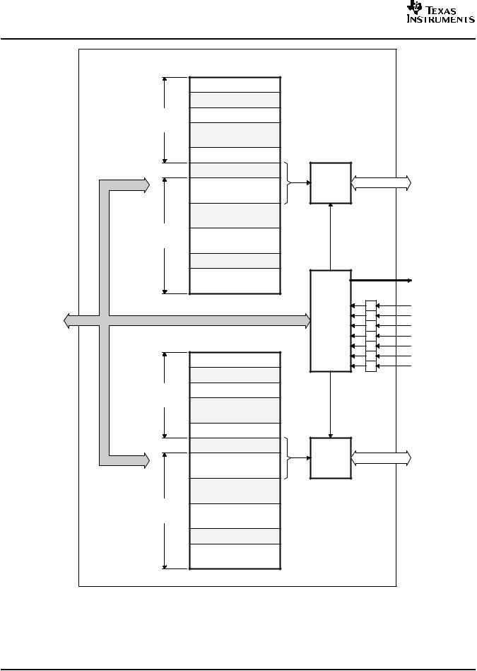
Figure 4-4 shows a block diagram of the dMAX controller.
Submit Documentation Feedback |
Peripheral and Electrical Specifications |
39 |
TMS320C6727B, TMS320C6726B, TMS320C6722B, TMS320C6720
Floating-Point Digital Signal Processors
SPRS370C–SEPTEMBER 2006–REVISED OCTOBER 2007 |
|
|
www.ti.com |
|
|
|
|
|
High-Priority PaRAM |
dMAX |
|
|
Event Entry #0 |
|
|
Event |
Event Entry #k |
|
|
Entry |
|
|
|
|
|
|
|
Table |
|
|
|
HiMAX |
|
|
|
RAM |
Event Entry #31 |
|
|
R/W |
|
HiMAX |
|
|
|
||
|
Reserved |
|
|
|
HiMAX |
Master |
|
|
|
||
|
|
Crossbar |
|
|
Transfer Entry #0 |
(MAX0) |
|
|
Switch |
||
|
|
||
|
|
|
Port |
Transfer |
|
High-Priority |
|
Entry |
|
|
|
Transfer Entry #k |
REQ |
|
|
Table |
|
||
|
|
|
|
|
|
|
Interrupt |
Control |
Transfer Entry #7 |
|
Lines to |
R/W |
|
|
the CPU |
|
|
Event |
|
To/From |
|
Encoder |
|
|
+ |
|
|
Crossbar |
|
|
|
|
Event and |
|
|
Switch |
|
|
|
|
Interrupt |
Events |
|
|
|
||
|
Low-Priority PaRAM |
Registers |
|
|
|
||
|
Event Entry #0 |
|
|
Event |
Event Entry #k |
|
|
Entry |
|
|
|
|
|
|
|
Table |
|
Low-Priority |
|
LoMAX |
|
REQ |
|
RAM |
Event Entry #31 |
|
|
R/W |
|
LoMAX |
|
|
|
||
|
Reserved |
|
|
|
LoMAX |
Master |
|
|
|
||
|
|
Crossbar |
|
|
Transfer Entry #0 |
(MAX1) |
|
|
Switch |
||
|
|
||
|
|
|
Port |
Transfer |
|
|
|
Entry |
Transfer Entry #k |
|
|
Table |
|
|
|
|
|
|
|
|
Transfer Entry #7 |
|
|
Figure 4-4. dMAX Controller Block Diagram
40 |
Peripheral and Electrical Specifications |
Submit Documentation Feedback |
TMS320C6727B, TMS320C6726B, TMS320C6722B, TMS320C6720
Floating-Point Digital Signal Processors
www.ti.com
SPRS370C–SEPTEMBER 2006–REVISED OCTOBER 2007
The dMAX controller comprises:
∙Event and interrupt processing registers
∙Event encoder
∙High-priority event Parameter RAM (PaRAM)
∙Low-priority event Parameter RAM (PaRAM)
∙Address-generation hardware for High-Priority Events – MAX0 (HiMAX)
∙Address-generation hardware for Low-Priority Events – MAX1 (LoMAX)
The TMS320C672x Peripheral Bus Structure can be described logically as a Crossbar Switch with five master ports and five slave ports. When accessing the slave ports, the MAX0 (HiMAX) module is always given the highest priority followed by the MAX1 (LoMAX) module. In other words, in case several masters (including MAX0 and MAX1) attempt to access same slave port concurrently, the MAX0 will be given the highest priority followed by MAX1.
Event signals are connected to bits of the dMAX Event Register (DER), and the bits in the DER reflect the current state of the event signals. An event is defined as a transition of the event signal. The dMAX Event Flag Register (DEFR) can be programmed, individually for each event signal, to capture either low-to-high or high-to-low transitions of the bits in the DER (event polarity is individually programmable).
An event is a synchronization signal that can be used: 1) to either trigger dMAX to start a transfer, or 2) to generate an interrupt to the CPU. All the events are sorted into two groups: low-priority event group and high-priority event group.
The High-Priority Data Movement Accelerator MAX0 (HiMAX) module is dedicated to serving requests coming from the high-priority event group. The Low-Priority Data Movement Accelerator MAX1 (LoMAX) module is dedicated to serving requests coming from the low-priority event group.
Each PaRAM contains two sections: the event entry table section and the transfer entry table section. An event entry describes an event type and associates the event to either one of transfer types or to an interrupt. In case an event entry associates the event to one of the transfer types, the event entry will contain a pointer to the specific transfer entry in the transfer entry table. The transfer table may contain up to eight transfer entries. A transfer entry specifies details required by the dMAX controller to perform the transfer. In case an event entry associates the event to an interrupt, the event entry specifies which interrupt should be generated to the CPU in case the event arrives.
Prior to enabling events and triggering a transfer, the event entry and transfer entry must be configured. The event entry must specify: type of transfer, transfer details (type of synchronization, reload, element size, etc.), and should include a pointer to the transfer entry. The transfer entry must specify: source, destination, counts, and indexes. If an event is sorted in the high-priority event group, the event entry and transfer entry must be specified in the high-priority Parameter RAM. If an event is sorted in the low-priority event group, the event entry and transfer entry must be specified in the low-priority parameter RAM.
The dMAX Event Flag Register (DEFR) captures up to 31 separate events; therefore, it is possible for events to occur simultaneously on the dMAX event inputs. In such cases, the event encoder resolves the order of processing. This mechanism sorts simultaneous events and sets the priority of the events. The dMAX controller can simultaneously process one event from each priority group. Therefore, the two highest-priority events (one from each group) can be processed at the same time.
An event-triggered dMAX transfer allows the submission of transfer requests to occur automatically based on system events, without any intervention by the CPU. The dMAX also includes support for CPU-initiated transfers for added control and robustness, and they can be used to start memory-to-memory transfers. To generate an event to the dMAX controller the CPU must create a transition on one of the bits from the dMAX Event Trigger (DETR) Register, which are mapped to the DER register.
Submit Documentation Feedback |
Peripheral and Electrical Specifications |
41 |

TMS320C6727B, TMS320C6726B, TMS320C6722B, TMS320C6720
Floating-Point Digital Signal Processors
www.ti.com
SPRS370C–SEPTEMBER 2006–REVISED OCTOBER 2007
Table 4-2 lists how the synchronization events are associated with event numbers in the dMAX controller.
Table 4-2. dMAX Peripheral Event Input Assignments
EVENT NUMBER |
EVENT ACRONYM |
EVENT DESCRIPTION |
0 |
DETR[0] |
The CPU triggers the event by creating appropriate transition (edge) on bit0 |
|
|
in DETR register. |
1 |
DETR[16] |
The CPU triggers the event by creating appropriate transition (edge) on bit16 |
|
|
in DETR register. |
2 |
RTIREQ0 |
RTI DMA REQ[0] |
3 |
RTIREQ1 |
RTI DMA REQ[1] |
4 |
MCASP0TX |
McASP0 TX DMA REQ |
5 |
MCASP0RX |
McASP0 RX DMA REQ |
6 |
MCASP1TX |
McASP1 TX DMA REQ |
7 |
MCASP1RX |
McASP1 RX DMA REQ |
8 |
MCASP2TX |
McASP2 TX DMA REQ |
9 |
MCASP2RX |
McASP2 RX DMA REQ |
10 |
DETR[1] |
The CPU triggers the event by creating appropriate transition (edge) on bit1 |
|
|
in DETR register. |
11 |
DETR[17] |
The CPU triggers the event by creating appropriate transition (edge) on bit17 |
|
|
in DETR register. |
12 |
UHPIINT |
UHPI CPU_INT |
13 |
SPI0RX |
SPI0 DMA_RX_REQ |
14 |
SPI1RX |
SPI1 DMA_RX_REQ |
15 |
RTIREQ2 |
RTI DMA REQ[2] |
16 |
RTIREQ3 |
RTI DMA REQ[3] |
17 |
DETR[2] |
The CPU triggers the event by creating appropriate transition (edge) on bit2 |
|
|
in DETR register. |
18 |
DETR[18] |
The CPU triggers the event by creating appropriate transition (edge) on bit18 |
|
|
in DETR register. |
19 |
I2C0XEVT |
I2C 0 Transmit Event |
20 |
I2C0REVT |
I2C 0 Receive Event |
21 |
I2C1XEVT |
I2C 1 Transmit Event |
22 |
I2C1REVT |
I2C 1 Receive Event |
23 |
DETR[3] |
The CPU triggers the event by creating appropriate transition (edge) on bit3 |
|
|
in DETR register. |
24 |
DETR[19] |
The CPU triggers the event by creating appropriate transition (edge) on bit19 |
|
|
in DETR register. |
25 |
Reserved |
|
26 |
MCASP0ERR |
AMUTEIN0 or McASP0 TX INT or McASP0 RX INT (error on McASP0) |
27 |
MCASP1ERR |
AMUTEIN1 or McASP1 TX INT or McASP1 RX INT (error on McASP1) |
28 |
MCASP2ERR |
AMUTEIN2 or McASP2 TX INT or McASP2 RX INT (error on McASP2) |
29 |
OVLREQ[0/1] |
Error on RTI |
30 |
DETR[20] |
The CPU triggers the event by creating appropriate transition (edge) on bit20 |
|
|
in DETR register. |
31 |
DETR[21] |
The CPU triggers the event by creating appropriate transition (edge) on bit21 |
|
|
in DETR register. |
42 |
Peripheral and Electrical Specifications |
Submit Documentation Feedback |