

TMS320C6727B, TMS320C6726B, TMS320C6722B, TMS320C6720
Floating-Point Digital Signal Processors
www.ti.com
SPRS370C–SEPTEMBER 2006–REVISED OCTOBER 2007
4.14 Serial Peripheral Interface Ports (SPI0, SPI1)
4.14.1 SPI Device-Specific Information
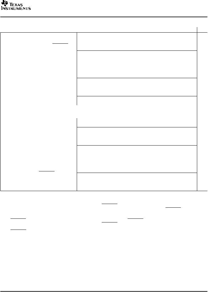
Figure 4-31 is a block diagram of the SPI module, which is a simple shift register and buffer plus control logic. Data is written to the shift register before transmission occurs and is read from the buffer at the end of transmission. The SPI can operate either as a master, in which case, it initiates a transfer and drives the SPIx_CLK pin, or as a slave. Four clock phase and polarity options are supported as well as many data formatting options.
Interrupt and
DMA Requests
|
|
|
|
SPIx_SIMO |
|
|
|
|
SPIx_SOMI |
Peripheral |
16-Bit Shift Register |
|
|
|
Configuration Bus |
|
|
SPIx_ENA |
|
|
|
GPIO |
State |
SPIx_SCS |
|
|
Machine |
||
|
|
Control |
||
|
16-Bit Buffer |
Clock |
|
|
|
(all pins) |
SPIx_CLK |
||
|
|
|
Control |
|
|
16-Bit Emulation Buffer |
|
|
|
|
|
|
|
|
|
C672x SPI Module |
|
|
|
Figure 4-31. Block Diagram of SPI Module
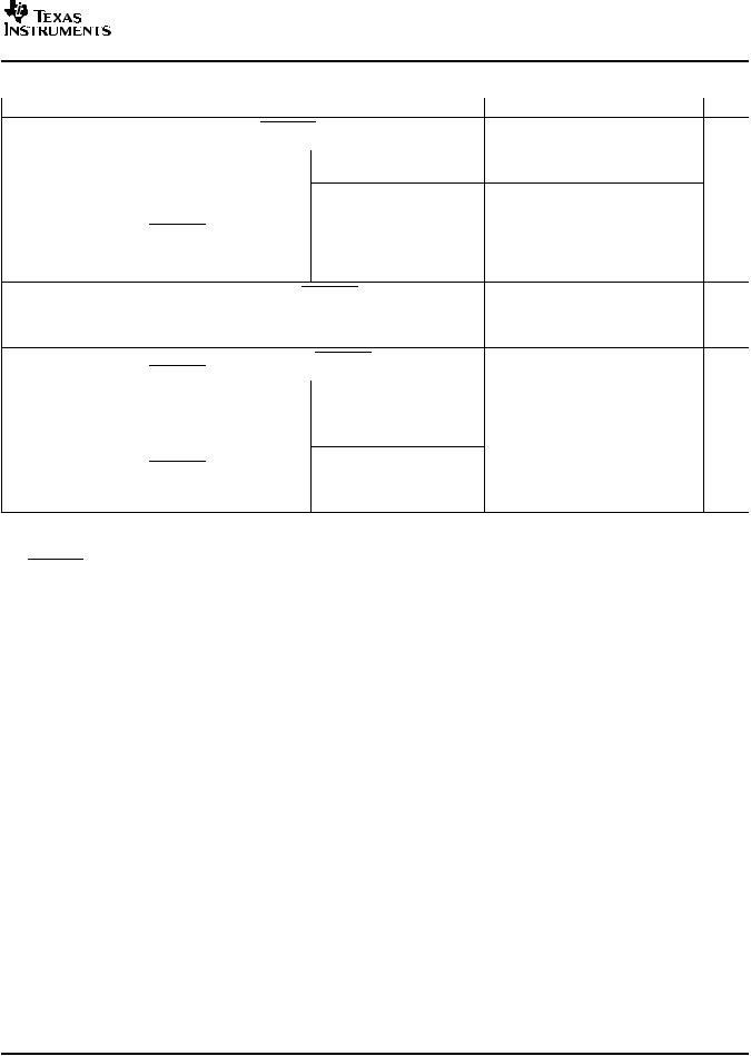
The SPI supports 3-, 4-, and 5-pin operation with three basic pins (SPIx_CLK, SPIx_SIMO, and SPIx_SOMI) and two optional pins (SPIx_SCS, SPIx_ENA).
The optional SPIx_SCS (Slave Chip Select) pin is most useful to enable in slave mode when there are other slave devices on the same SPI port. The C672x will only shift data and drive the SPIx_SOMI pin when SPIx_SCS is held low.
In slave mode, SPIx_ENA is an optional output and can be driven in either a push-pull or open-drain manner. The SPIx_ENA output provides the status of the internal transmit buffer (SPIDAT0/1 registers). In four-pin mode with the enable option, SPIx_ENA is asserted only when the transmit buffer is full, indicating that the slave is ready to begin another transfer. In five-pin mode, the SPIx_ENA is additionally qualified by SPIx_SCS being asserted. This allows a single handshake line to be shared by multiple slaves on the same SPI bus.
In master mode, the SPIx_ENA pin is an optional input and the master can be configured to delay the start of the next transfer until the slave asserts SPIx_ENA. The addition of this handshake signal simplifies SPI communications and, on average, increases SPI bus throughput since the master does not need to delay each transfer long enough to allow for the worst-case latency of the slave device. Instead, each transfer can begin as soon as both the master and slave have actually serviced the previous SPI transfer.
Submit Documentation Feedback |
Peripheral and Electrical Specifications |
81 |

TMS320C6727B, TMS320C6726B, TMS320C6722B, TMS320C6720
Floating-Point Digital Signal Processors
www.ti.com
SPRS370C–SEPTEMBER 2006–REVISED OCTOBER 2007
SPIx_SCS
SPIx_ENA
SPIx_CLK
SPIx_SOMI
SPIx_SIMO
MASTER SPI
Optional − Slave Chip Select |
Optional Enable (Ready) |
SPIx_SCS
SPIx_ENA
SPIx_CLK
SPIx_SOMI
SPIx_SIMO
SLAVE SPI
Figure 4-32. Illustration of SPI Master-to-SPI Slave Connection
82 |
Peripheral and Electrical Specifications |
Submit Documentation Feedback |

TMS320C6727B, TMS320C6726B, TMS320C6722B, TMS320C6720
Floating-Point Digital Signal Processors
www.ti.com
SPRS370C–SEPTEMBER 2006–REVISED OCTOBER 2007
4.14.2 SPI Peripheral Registers Description(s)
Table 4-26 is a list of the SPI registers.
Table 4-26. SPIx Configuration Registers
SPI0 |
SPI1 |
REGISTER NAME |
DESCRIPTION |
|
BYTE ADDRESS |
BYTE ADDRESS |
|||
|
|
|||
0x4700 0000 |
0x4800 0000 |
SPIGCR0 |
Global Control Register 0 |
|
0x4700 0004 |
0x4800 0004 |
SPIGCR1 |
Global Control Register 1 |
|
0x4700 0008 |
0x4800 0008 |
SPIINT0 |
Interrupt Register |
|
0x4700 000C |
0x4800 000C |
SPILVL |
Interrupt Level Register |
|
0x4700 0010 |
0x4800 0010 |
SPIFLG |
Flag Register |
|
0x4700 0014 |
0x4800 0014 |
SPIPC0 |
Pin Control Register 0 (Pin Function) |
|
0x4700 0018 |
0x4800 0018 |
SPIPC1 |
Pin Control Register 1 (Pin Direction) |
|
0x4700 001C |
0x4800 001C |
SPIPC2 |
Pin Control Register 2 (Pin Data In) |
|
0x4700 0020 |
0x4800 0020 |
SPIPC3 |
Pin Control Register 3 (Pin Data Out) |
|
0x4700 0024 |
0x4800 0024 |
SPIPC4 |
Pin Control Register 4 (Pin Data Set) |
|
0x4700 0028 |
0x4800 0028 |
SPIPC5 |
Pin Control Register 5 (Pin Data Clear) |
|
0x4700 002C |
0x4800 002C |
Reserved |
Reserved - Do not write to this register |
|
0x4700 0030 |
0x4800 0030 |
Reserved |
Reserved - Do not write to this register |
|
0x4700 0034 |
0x4800 0034 |
Reserved |
Reserved - Do not write to this register |
|
0x4700 0038 |
0x4800 0038 |
SPIDAT0 |
Shift Register 0 (without format select) |
|
0x4700 003C |
0x4800 003C |
SPIDAT1 |
Shift Register 1 (with format select) |
|
0x4700 0040 |
0x4800 0040 |
SPIBUF |
Buffer Register |
|
0x4700 0044 |
0x4800 0044 |
SPIEMU |
Emulation Register |
|
0x4700 0048 |
0x4800 0048 |
SPIDELAY |
Delay Register |
|
0x4700 004C |
0x4800 004C |
SPIDEF |
Default Chip Select Register |
|
0x4700 0050 |
0x4800 0050 |
SPIFMT0 |
Format Register 0 |
|
0x4700 0054 |
0x4800 0054 |
SPIFMT1 |
Format Register 1 |
|
0x4700 0058 |
0x4800 0058 |
SPIFMT2 |
Format Register 2 |
|
0x4700 005C |
0x4800 005C |
SPIFMT3 |
Format Register 3 |
|
0x4700 0060 |
0x4800 0060 |
TGINTVECT0 |
Interrupt Vector for SPI INT0 |
|
0x4700 0064 |
0x4800 0064 |
TGINTVECT1 |
Interrupt Vector for SPI INT1 |
Submit Documentation Feedback |
Peripheral and Electrical Specifications |
83 |

TMS320C6727B, TMS320C6726B, TMS320C6722B, TMS320C6720
Floating-Point Digital Signal Processors
www.ti.com
SPRS370C–SEPTEMBER 2006–REVISED OCTOBER 2007
4.14.3 SPI Electrical Data/Timing
4.14.3.1 Serial Peripheral Interface (SPI) Timing
Table 4-27 through Table 4-34 assume testing over recommended operating conditions (see Figure 4-33 through Figure 4-36).
Table 4-27. General Timing Requirements for SPIx Master Modes(1)
 NO.
NO. 
1tc(SPC)M
2tw(SPCH)M
3tw(SPCL)M
4 td(SIMO_SPC)M
5 td(SPC_SIMO)M
6 toh(SPC_SIMO)M
7 tsu(SOMI_SPC)M
8 tih(SPC_SOMI)M
Cycle Time, SPIx_CLK, All Master Modes
Pulse Width High, SPIx_CLK, All Master Modes
Pulse Width Low, SPIx_CLK, All Master Modes
Delay, initial data bit valid
on SPIx_SIMO to initial edge on SPIx_CLK(2)
Delay, subsequent bits valid on SPIx_SIMO after transmit edge of SPIx_CLK
Output hold time, SPIx_SIMO valid after
receive edge of SPIxCLK, except for final bit(3)
Input Setup Time,
SPIx_SOMI valid before receive edge of SPIx_CLK
Input Hold Time, SPIx_SOMI valid after receive edge of SPIx_CLK
Polarity = 0, Phase = 0, to SPIx_CLK rising
Polarity = 0, Phase = 1, to SPIx_CLK rising
Polarity = 1, Phase = 0, to SPIx_CLK falling
Polarity = 1, Phase = 1, to SPIx_CLK falling
Polarity = 0, Phase = 0, from SPIx_CLK rising
Polarity = 0, Phase = 1, from SPIx_CLK falling
Polarity = 1, Phase = 0, from SPIx_CLK falling
Polarity = 1, Phase = 1, from SPIx_CLK rising
Polarity = 0, Phase = 0, from SPIx_CLK falling
Polarity = 0, Phase = 1, from SPIx_CLK rising
Polarity = 1, Phase = 0, from SPIx_CLK rising
Polarity = 1, Phase = 1, from SPIx_CLK falling
Polarity = 0, Phase = 0, to SPIx_CLK falling
Polarity = 0, Phase = 1, to SPIx_CLK rising
Polarity = 1, Phase = 0, to SPIx_CLK rising
Polarity = 1, Phase = 1, to SPIx_CLK falling
Polarity = 0, Phase = 0, from SPIx_CLK falling
Polarity = 0, Phase = 1, from SPIx_CLK rising
Polarity = 1, Phase = 0, from SPIx_CLK rising
Polarity = 1, Phase = 1, from SPIx_CLK falling
MIN
greater of 8P or 100 ns
 greater of 4P or 45 ns greater of 4P or 45 ns
4P
0.5tc(SPC)M + 4P
4P
0.5tc(SPC)M + 4P
0.5tc(SPC)M – 10
0.5tc(SPC)M – 10
0.5tc(SPC)M – 10
0.5tc(SPC)M – 10
0.5P + 15
0.5P + 15
0.5P + 15
0.5P + 15
0.5P + 5
0.5P + 5
0.5P + 5
0.5P + 5
MAX  UNIT
UNIT 
256P ns
ns
ns
ns
15
15  ns
ns
15
15
ns
ns
ns
(1)P = SYSCLK2 period
(2)First bit may be MSB or LSB depending upon SPI configuration. MO(0) refers to first bit and MO(n) refers to last bit output on SPIx_SIMO. MI(0) refers to the first bit input and MI(n) refers to the last bit input on SPIx_SOMI.
(3)The final data bit will be held on the SPIx_SIMO pin until the SPIDAT0 or SPIDAT1 register is written with new data.
84 |
Peripheral and Electrical Specifications |
Submit Documentation Feedback |

TMS320C6727B, TMS320C6726B, TMS320C6722B, TMS320C6720
Floating-Point Digital Signal Processors
www.ti.com
SPRS370C–SEPTEMBER 2006–REVISED OCTOBER 2007
Table 4-28. General Timing Requirements for SPIx Slave Modes(1)
 NO.
NO. 
9 tc(SPC)S
10tw(SPCH)S
11tw(SPCL)S
12 tsu(SOMI_SPC)S
13 td(SPC_SOMI)S
14 toh(SPC_SOMI)S
15 tsu(SIMO_SPC)S
16 tih(SPC_SIMO)S
Cycle Time, SPIx_CLK, All Slave Modes
Pulse Width High, SPIx_CLK, All Slave Modes
Pulse Width Low, SPIx_CLK, All Slave Modes
Setup time, transmit data written to SPI and output onto SPIx_SOMI pin before
initial clock edge from master.(2)(3)
Delay, subsequent bits valid on SPIx_SOMI after transmit edge of SPIx_CLK
Output hold time, SPIx_SOMI valid after
receive edge of SPIxCLK, except for final bit(4)
Input Setup Time, SPIx_SIMO valid before receive edge of SPIx_CLK
Input Hold Time, SPIx_SIMO valid after receive edge of SPIx_CLK
Polarity = 0, Phase = 0, to SPIx_CLK rising
Polarity = 0, Phase = 1, to SPIx_CLK rising
Polarity = 1, Phase = 0, to SPIx_CLK falling
Polarity = 1, Phase = 1, to SPIx_CLK falling
Polarity = 0, Phase = 0, from SPIx_CLK rising
Polarity = 0, Phase = 1, from SPIx_CLK falling
Polarity = 1, Phase = 0, from SPIx_CLK falling
Polarity = 1, Phase = 1, from SPIx_CLK rising
Polarity = 0, Phase = 0, from SPIx_CLK falling
Polarity = 0, Phase = 1, from SPIx_CLK rising
Polarity = 1, Phase = 0, from SPIx_CLK rising
Polarity = 1, Phase = 1, from SPIx_CLK falling
Polarity = 0, Phase = 0, to SPIx_CLK falling
Polarity = 0, Phase = 1, to SPIx_CLK rising
Polarity = 1, Phase = 0, to SPIx_CLK rising
Polarity = 1, Phase = 1, to SPIx_CLK falling
Polarity = 0, Phase = 0, from SPIx_CLK falling
Polarity = 0, Phase = 1, from SPIx_CLK rising
Polarity = 1, Phase = 0, from SPIx_CLK rising
Polarity = 1, Phase = 1, from SPIx_CLK falling
MIN
greater of 8P or 100 ns
greater of 4P or 45 ns
greater of 4P or 45 ns
2P
2P
2P
2P
0.5tc(SPC)S – 10
0.5tc(SPC)S – 10
0.5tc(SPC)S – 10
0.5tc(SPC)S – 10
0.5P + 15
0.5P + 15
0.5P + 15
0.5P + 15
0.5P + 5
0.5P + 5
0.5P + 5
0.5P + 5
MAX  UNIT
UNIT 
256P ns
ns
ns
ns
2P + 15
2P + 15  ns
ns
2P + 15
2P + 15
ns
ns
ns
(1)P = SYSCLK2 period
(2)First bit may be MSB or LSB depending upon SPI configuration. SO(0) refers to first bit and SO(n) refers to last bit output on SPIx_SOMI. SI(0) refers to the first bit input and SI(n) refers to the last bit input on SPIx_SIMO.
(3)Measured from the termination of the write of new data to the SPI module, as evidenced by new output data appearing on the SPIx_SOMI pin. In analyzing throughput requirements, additional internal bus cycles must be accounted for to allow data to be written to the SPI module by either the DSP CPU or the dMAX.
(4)The final data bit will be held on the SPIx_SOMI pin until the SPIDAT0 or SPIDAT1 register is written with new data.
Submit Documentation Feedback |
Peripheral and Electrical Specifications |
85 |

TMS320C6727B, TMS320C6726B, TMS320C6722B, TMS320C6720 |
|
|
Floating-Point Digital Signal Processors |
|
www.ti.com |
SPRS370C–SEPTEMBER 2006–REVISED OCTOBER 2007 |
|
|
Table 4-29. Additional(1) SPI Master Timings, 4-Pin Enable Option(2)(3) |
|
|
NO. |
MIN |
MAX UNIT |
Delay from slave assertion of
17 td(ENA_SPC)M SPIx_ENA active to first SPIx_CLK from master.(4)
Polarity = 0, Phase = 0, to SPIx_CLK rising
Polarity = 0, Phase = 1, to SPIx_CLK rising
Polarity = 1, Phase = 0, to SPIx_CLK falling
Polarity = 1, Phase = 1, to SPIx_CLK falling
Polarity = 0, Phase = 0, from SPIx_CLK falling
3P |
+ 15 |
0.5tc(SPC)M + 3P |
+ 15 |
|
ns |
3P |
+ 15 |
0.5tc(SPC)M + 3P |
+ 15 |
0.5tc(SPC)M 
Max delay for slave to deassert
SPIx_ENA after final SPIx_CLK 18 td(SPC_ENA)M edge to ensure master does not
begin the next transfer.(5)
Polarity = 0, Phase = 1, from SPIx_CLK falling
Polarity = 1, Phase = 0, from SPIx_CLK rising
0
ns
0.5tc(SPC)M
Polarity = 1, Phase = 1,
0
from SPIx_CLK rising
(1)These parameters are in addition to the general timings for SPI master modes (Table 4-27).
(2)P = SYSCLK2 period
(3)Figure shows only Polarity = 0, Phase = 0 as an example. Table gives parameters for all four master clocking modes.
(4)In the case where the master SPI is ready with new data before SPIx_ENA assertion.
(5)In the case where the master SPI is ready with new data before SPIx_ENA deassertion.
Table 4-30. Additional(1) SPI Master Timings, 4-Pin Chip Select Option(2)(3)
 NO.
NO. 
19 td(SCS_SPC)M
20 td(SPC_SCS)M
Delay from SPIx_SCS active to first SPIx_CLK(4)(5)
Delay from final SPIx_CLK edge
to master deasserting SPIx_SCS
(6)(7)
Polarity = 0, Phase = 0, to SPIx_CLK rising
Polarity = 0, Phase = 1, to SPIx_CLK rising
Polarity = 1, Phase = 0, to SPIx_CLK falling
Polarity = 1, Phase = 1, to SPIx_CLK falling
Polarity = 0, Phase = 0, from SPIx_CLK falling
Polarity = 0, Phase = 1, from SPIx_CLK falling
Polarity = 1, Phase = 0, from SPIx_CLK rising
Polarity = 1, Phase = 1, from SPIx_CLK rising
|
MIN |
MAX UNIT |
2P |
– 10 |
|
0.5tc(SPC)M + 2P |
– 10 |
ns |
|
|
|
2P |
– 10 |
|
0.5tc(SPC)M + 2P |
– 10 |
|
0.5tc(SPC)M
0
ns
0.5tc(SPC)M
0
(1)These parameters are in addition to the general timings for SPI master modes (Table 4-27).
(2)P = SYSCLK2 period
(3)Figure shows only Polarity = 0, Phase = 0 as an example. Table gives parameters for all four master clocking modes.
(4)In the case where the master SPI is ready with new data before SPIx_SCS assertion.
(5)This delay can be increased under software control by the register bit field SPIDELAY.C2TDELAY[4:0].
(6)Except for modes when SPIDAT1.CSHOLD is enabled and there is additional data to transmit. In this case, SPIx_SCS will remain asserted.
(7)This delay can be increased under software control by the register bit field SPIDELAY.T2CDELAY[4:0].
86 |
Peripheral and Electrical Specifications |
Submit Documentation Feedback |
TMS320C6727B, TMS320C6726B, TMS320C6722B, TMS320C6720
Floating-Point Digital Signal Processors
www.ti.com
SPRS370C–SEPTEMBER 2006–REVISED OCTOBER 2007
Table 4-31. Additional(1) SPI Master Timings, 5-Pin Option(2)(3)
 NO.
NO. 
18 td(SPC_ENA)M
20 td(SPC_SCS)M
21 td(SCSL_ENAL)M
Max delay for slave to deassert SPIx_ENA after final SPIx_CLK edge to ensure master does not begin the next
transfer.(4)
Delay from final SPIx_CLK edge to
master deasserting SPIx_SCS (5)(6)
Polarity = 0, Phase = 0, from SPIx_CLK falling
Polarity = 0, Phase = 1, from SPIx_CLK falling
Polarity = 1, Phase = 0, from SPIx_CLK rising
Polarity = 1, Phase = 1, from SPIx_CLK rising
Polarity = 0, Phase = 0, from SPIx_CLK falling
Polarity = 0, Phase = 1, from SPIx_CLK falling
Polarity = 1, Phase = 0, from SPIx_CLK rising
Polarity = 1, Phase = 1, from SPIx_CLK rising
Max delay for slave SPI to drive SPIx_ENA valid after master asserts SPIx_SCS to delay the master from beginning the next transfer.
MIN |
MAX |
UNIT |
|
0.5tc(SPC)M |
|
|
0 |
|
|
|
ns |
|
0.5tc(SPC)M |
|
|
0 |
|
0.5tc(SPC)M |
|
|
0 |
|
|
|
|
ns |
0.5tc(SPC)M |
|
|
0 |
|
|
|
0.5P |
ns |
22 td(SCS_SPC)M
23 td(ENA_SPC)M
Delay from SPIx_SCS
active to first SPIx_CLK(7)(8)(9)
Delay from assertion of
SPIx_ENA low to first SPIx_CLK edge.(10)
Polarity = 0, Phase = 0, to SPIx_CLK rising
Polarity = 0, Phase = 1, to SPIx_CLK rising
Polarity = 1, Phase = 0, to SPIx_CLK falling
Polarity = 1, Phase = 1, to SPIx_CLK falling
Polarity = 0, Phase = 0, to SPIx_CLK rising
Polarity = 0, Phase = 1, to SPIx_CLK rising
Polarity = 1, Phase = 0, to SPIx_CLK falling
Polarity = 1, Phase = 1, to SPIx_CLK falling
2P – 10
0.5tc(SPC)M + 2P – 10
 ns 2P – 10
0.5tc(SPC)M + 2P – 10
3P |
+ 15 |
0.5tc(SPC)M + 3P |
+ 15 |
|
ns |
3P |
+ 15 |
0.5tc(SPC)M + 3P |
+ 15 |
(1)These parameters are in addition to the general timings for SPI master modes (Table 4-27).
(2)P = SYSCLK2 period
(3)Figure shows only Polarity = 0, Phase = 0 as an example. Table gives parameters for all four master clocking modes.
(4)In the case where the master SPI is ready with new data before SPIx_ENA deassertion.
(5)Except for modes when SPIDAT1.CSHOLD is enabled and there is additional data to transmit. In this case, SPIx_SCS will remain asserted.
(6)This delay can be increased under software control by the register bit field SPIDELAY.T2CDELAY[4:0].
(7)If SPIx_ENA is asserted immediately such that the transmission is not delayed by SPIx_ENA.
(8)In the case where the master SPI is ready with new data before SPIx_SCS assertion.
(9)This delay can be increased under software control by the register bit field SPIDELAY.C2TDELAY[4:0].
(10)If SPIx_ENA was initially deasserted high and SPIx_CLK is delayed.
Submit Documentation Feedback |
Peripheral and Electrical Specifications |
87 |

TMS320C6727B, TMS320C6726B, TMS320C6722B, TMS320C6720
Floating-Point Digital Signal Processors
www.ti.com
SPRS370C–SEPTEMBER 2006–REVISED OCTOBER 2007
Table 4-32. Additional(1) SPI Slave Timings, 4-Pin Enable Option(2)(3)
 NO.
NO. 
Delay from final
24 td(SPC_ENAH)S SPIx_CLK edge to slave deasserting SPIx_ENA.
Polarity = 0, Phase = 0, from SPIx_CLK falling
Polarity = 0, Phase = 1, from SPIx_CLK falling
Polarity = 1, Phase = 0, from SPIx_CLK rising
Polarity = 1, Phase = 1, from SPIx_CLK rising
MIN |
|
MAX UNIT |
P – 10 |
3P |
+ 15 |
0.5tc(SPC)M + P – 10 |
0.5tc(SPC)M + 3P |
+ 15 |
|
|
ns |
P – 10 |
3P |
+ 15 |
0.5tc(SPC)M + P – 10 |
0.5tc(SPC)M + 3P |
+ 15 |
(1)These parameters are in addition to the general timings for SPI slave modes (Table 4-28).
(2)P = SYSCLK2 period
(3)Figure shows only Polarity = 0, Phase = 0 as an example. Table gives parameters for all four slave clocking modes.
Table 4-33. Additional(1) SPI Slave Timings, 4-Pin Chip Select Option(2)(3)
NO.
25 td(SCSL_SPC)S
26 td(SPC_SCSH)S
27tena(SCSL_SOMI)S
28tdis(SCSH_SOMI)S
Required delay from SPIx_SCS asserted at slave to first SPIx_CLK edge at slave.
Required delay from final SPIx_CLK edge before SPIx_SCS is deasserted.
Polarity = 0, Phase = 0, from SPIx_CLK falling
Polarity = 0, Phase = 1, from SPIx_CLK falling
Polarity = 1, Phase = 0, from SPIx_CLK rising
Polarity = 1, Phase = 1, from SPIx_CLK rising
Delay from master asserting SPIx_SCS to slave driving SPIx_SOMI valid
Delay from master deasserting SPIx_SCS to slave 3-stating SPIx_SOMI
MIN |
MAX UNIT |
P |
ns |
0.5tc(SPC)M + P + 10
P + 10
ns
0.5tc(SPC)M + P + 10
P + 10
P + 15 |
ns |
P + 15 |
ns |
(1)These parameters are in addition to the general timings for SPI slave modes (Table 4-28).
(2)P = SYSCLK2 period
(3)Figure shows only Polarity = 0, Phase = 0 as an example. Table gives parameters for all four slave clocking modes.
88 |
Peripheral and Electrical Specifications |
Submit Documentation Feedback |
TMS320C6727B, TMS320C6726B, TMS320C6722B, TMS320C6720
Floating-Point Digital Signal Processors
www.ti.com
SPRS370C–SEPTEMBER 2006–REVISED OCTOBER 2007
Table 4-34. Additional(1) SPI Slave Timings, 5-Pin Option(2)(3)
NO.
25 td(SCSL_SPC)S
26 td(SPC_SCSH)S
27tena(SCSL_SOMI)S
28tdis(SCSH_SOMI)S
29tena(SCSL_ENA)S
30 tdis(SPC_ENA)S
Required delay from SPIx_SCS asserted at slave to first SPIx_CLK edge at slave.
Required delay from final SPIx_CLK edge before SPIx_SCS is deasserted.
Polarity = 0, Phase = 0, from SPIx_CLK falling
Polarity = 0, Phase = 1, from SPIx_CLK falling
Polarity = 1, Phase = 0, from SPIx_CLK rising
Polarity = 1, Phase = 1, from SPIx_CLK rising
Delay from master asserting SPIx_SCS to slave driving SPIx_SOMI valid
Delay from master deasserting SPIx_SCS to slave 3-stating SPIx_SOMI
Delay from master deasserting SPIx_SCS to slave driving SPIx_ENA valid
Delay from final clock receive edge on SPIx_CLK to slave
3-stating or driving high SPIx_ENA.(4)
Polarity = 0, Phase = 0, from SPIx_CLK falling
Polarity = 0, Phase = 1, from SPIx_CLK rising
Polarity = 1, Phase = 0, from SPIx_CLK rising
Polarity = 1, Phase = 1, from SPIx_CLK falling
MIN |
MAX |
UNIT |
P |
|
ns |
0.5tc(SPC)M + P + 10 |
|
|
P + 10 |
|
|
|
|
ns |
0.5tc(SPC)M + P + 10 |
|
|
P + 10 |
|
|
|
P + 10 |
ns |
|
P + 10 |
ns |
|
15 |
ns |
|
2P + 15 |
|
2P + 15  ns
ns
2P + 15
2P + 15
(1)These parameters are in addition to the general timings for SPI slave modes (Table 4-28).
(2)P = SYSCLK2 period
(3)Figure shows only Polarity = 0, Phase = 0 as an example. Table gives parameters for all four slave clocking modes.
(4)SPIx_ENA is driven low after the transmission completes if the SPIINT0.ENABLE_HIGHZ bit is programmed to 0. Otherwise it is 3-stated. If 3-stated, an external pullup resistor should be used to provide a valid level to the master. This option is useful when tying several SPI slave devices to a single master.
Submit Documentation Feedback |
Peripheral and Electrical Specifications |
89 |

TMS320C6727B, TMS320C6726B, TMS320C6722B, TMS320C6720
Floating-Point Digital Signal Processors
www.ti.com
SPRS370C–SEPTEMBER 2006–REVISED OCTOBER 2007
|
1 |
|
MASTER MODE |
|
|
2 |
3 |
POLARITY = 0 PHASE = 0 |
|
|
|
|
||
SPIx_CLK |
|
|
|
|
|
4 |
5 |
6 |
|
SPI_SIMO |
MO(0) |
MO(1) |
MO(n−1) |
MO(n) |
|
7 |
8 |
|
|
SPI_SOMI |
MI(0) |
MI(1) |
MI(n−1) |
MI(n) |
|
|
|
|
|
MASTER MODE |
|
4 |
|
|
|
POLARITY = 0 PHASE = 1 |
|
|
|
|
|
|
SPIx_CLK |
|
|
|
|
|
|
|
5 |
|
6 |
|
SPI_SIMO |
MO(0) |
|
MO(1) |
MO(n−1) |
MO(n) |
|
7 |
8 |
|
|
|
SPI_SOMI |
MI(0) |
|
MI(1) |
MI(n−1) |
MI(n) |
|
4 |
|
|
|
MASTER MODE |
|
|
|
|
|
|
||
|
|
|
|
|
POLARITY = 1 PHASE = 0 |
|
SPIx_CLK |
|
|
|
|
|
|
|
|
|
5 |
|
6 |
|
SPI_SIMO |
|
MO(0) |
|
MO(1) |
MO(n−1) |
MO(n) |
|
|
7 |
8 |
|
|
|
SPI_SOMI |
|
MI(0) |
|
MI(1) |
MI(n−1) |
MI(n) |
|
|
|
|
|
MASTER MODE |
|
|
|
|
|
|
POLARITY = 1 PHASE = 1 |
|
SPIx_CLK |
|
|
|
|
|
|
|
4 |
|
5 |
6 |
|
|
SPI_SIMO |
MO(0) |
|
MO(1) |
|
MO(n−1) |
MO(n) |
|
7 |
8 |
|
|
|
|
SPI_SOMI |
MI(0) |
|
MI(1) |
|
MI(n−1) |
MI(n) |
Figure 4-33. SPI Timings—Master Mode
90 |
Peripheral and Electrical Specifications |
Submit Documentation Feedback |
TMS320C6727B, TMS320C6726B, TMS320C6722B, TMS320C6720
Floating-Point Digital Signal Processors
www.ti.com
|
|
|
SPRS370C–SEPTEMBER 2006–REVISED OCTOBER 2007 |
|
|
9 |
|
SLAVE MODE |
|
12 |
10 |
11 |
POLARITY = 0 PHASE = 0 |
|
|
|
|||
SPIx_CLK |
|
|
|
|
|
15 |
16 |
|
|
SPI_SIMO |
SI(0) |
SI(1) |
SI(n−1) |
SI(n) |
|
|
13 |
14 |
|
|
|
|
|
|
SPI_SOMI |
SO(0) |
SO(1) |
SO(n−1) |
SO(n) |
|
12 |
|
|
|
SLAVE MODE |
|
|
|
|
|
POLARITY = 0 PHASE = 1 |
SPIx_CLK |
|
|
|
|
|
|
15 |
16 |
|
|
|
SPI_SIMO |
SI(0) |
|
SI(1) |
SI(n−1) |
SI(n) |
|
|
13 |
14 |
|
|
SPI_SOMI |
SO(0) |
SO(1) |
SO(n−1) |
SO(n) |
|
|
12 |
|
SLAVE MODE |
|
|
|
POLARITY = 1 PHASE = 0 |
||
|
|
|
||
SPIx_CLK |
|
|
|
|
|
15 |
16 |
|
|
SPI_SIMO |
SI(0) |
SI(1) |
SI(n−1) |
SI(n) |
|
|
13 |
14 |
|
SPI_SOMI |
SO(0) |
SO(1) |
SO(n−1) |
SO(n) |
|
12 |
|
|
|
|
SLAVE MODE |
|
|
|
|
|
POLARITY = 1 PHASE = 1 |
|
|
|
|
|
|
|
|
SPIx_CLK |
|
|
|
|
|
|
|
15 |
16 |
|
|
|
|
SPI_SIMO |
|
SI(0) |
SI(1) |
|
SI(n−1) |
SI(n) |
|
|
|
13 |
14 |
|
|
SPI_SOMI |
SO(0) |
SO(1) |
SO(n−1) |
SO(n) |
||
Figure 4-34. SPI Timings—Slave Mode
Submit Documentation Feedback |
Peripheral and Electrical Specifications |
91 |

TMS320C6727B, TMS320C6726B, TMS320C6722B, TMS320C6720
Floating-Point Digital Signal Processors
www.ti.com
SPRS370C–SEPTEMBER 2006–REVISED OCTOBER 2007
|
MASTER MODE 4 PIN WITH ENABLE |
|
||
|
17 |
|
|
18 |
SPIx_CLK |
|
|
|
|
SPI_SIMO |
MO(0) |
MO(1) |
MO(n−1) |
MO(n) |
SPI_SOMI |
MI(0) |
MI(1) |
MI(n−1) |
MI(n) |
SPIx_ENA |
|
|
|
|
|
MASTER MODE 4 PIN WITH CHIP SELECT |
|||
|
19 |
|
|
20 |
SPIx_CLK SPI_SIMO SPI_SOMI
SPIx_SCS
MO(0) |
MO(1) |
MO(n−1) |
MO(n) |
 MI(0)
MI(0)  MI(1)
MI(1) 

 MI(n−1)
 MI(n)
MI(n)
|
22 |
MASTER MODE 5 PIN |
20 |
||
|
|
23 |
|
MO(1) |
|
|
|
|
|
18 |
|
SPIx_CLK |
|
|
|
|
|
SPI_SIMO |
|
MO(0) |
|
MO(n−1) |
MO(n) |
SPI_SOMI |
|
|
|
|
|
|
21 |
MI(0) |
MI(1) |
MI(n−1) |
MI(n) |
SPIx_ENA |
DESEL(A) |
|
|
|
DESEL(A) |
SPIx_SCS |
|
|
|
|
|
A.DESELECTED IS PROGRAMMABLE EITHER HIGH OR 3−ST ATE (REQUIRES EXTERNAL PULLUP)
Figure 4-35. SPI Timings—Master Mode (4-Pin and 5-Pin)
92 |
Peripheral and Electrical Specifications |
Submit Documentation Feedback |

TMS320C6727B, TMS320C6726B, TMS320C6722B, TMS320C6720
Floating-Point Digital Signal Processors
www.ti.com
|
|
|
|
|
|
SPRS370C–SEPTEMBER 2006–REVISED OCTOBER 2007 |
|
SLAVE MODE 4 PIN WITH ENABLE |
|||||
|
|
|
|
|
|
24 |
SPIx_CLK |
|
|
|
|
|
|
SPI_SOMI |
|
SO(0) |
SO(1) |
SO(n−1) |
SO(n) |
|
SPI_SIMO |
|
|
|
|
|
|
SPIx_ENA |
|
SI(0) |
SI(1) |
SI(n−1) |
SI(n) |
|
|
SLAVE MODE 4 PIN WITH CHIP SELECT |
|||||
|
|
25 |
|
|
|
26 |
SPIx_CLK |
|
|
|
|
|
|
|
|
27 |
SO(n−1) |
|
28 |
|
|
|
|
|
|
||
SPI_SOMI |
|
SO(0) |
SO(1) |
|
|
SO(n) |
SPI_SIMO |
|
|
|
|
|
|
SPIx_SCS |
|
SI(0) |
SI(1) |
SI(n−1) |
|
SI(n) |
|
SLAVE MODE 5 PIN |
|
|
26 |
||
|
|
|
|
|
|
|
|
25 |
|
|
|
|
30 |
SPIx_CLK |
|
|
|
|
|
|
|
27 |
SO(1) |
|
|
28 |
|
SPI_SOMI |
|
SO(0) |
|
SO(n−1) |
SO(n) |
|
SPI_SIMO |
|
|
|
|
|
|
|
29 |
SI(0) |
SI(1) |
SI(n−1) |
SI(n) |
|
SPIx_ENA |
DESEL(A) |
|
|
|
|
DESEL(A) |
|
|
|
|
|
||
SPIx_SCS |
|
|
|
|
|
|
A.DESELECTED IS PROGRAMMABLE EITHER HIGH OR 3−ST ATE (REQUIRES EXTERNAL PULLUP)
Figure 4-36. SPI Timings—Slave Mode (4-Pin and 5-Pin)
Submit Documentation Feedback |
Peripheral and Electrical Specifications |
93 |