

TMS320C6727B, TMS320C6726B, TMS320C6722B, TMS320C6720
Floating-Point Digital Signal Processors
www.ti.com
SPRS370C–SEPTEMBER 2006–REVISED OCTOBER 2007
2 Device Overview
2.1 Device Characteristics
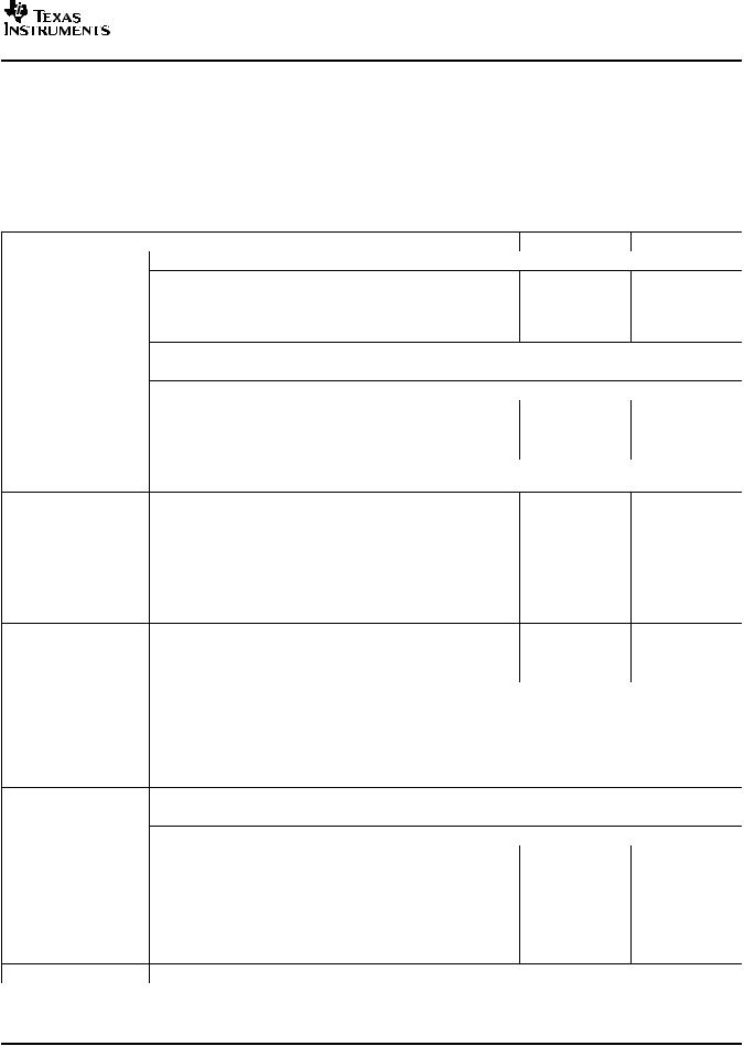
Table 2-1 provides an overview of the C672x DSPs. The table shows significant features of each device, including the capacity of on-chip memory, the peripherals, the execution time, and the package type with pin count.
Table 2-1. Characteristics of the C672x Processors
HARDWARE FEATURES |
C6727B |
C6726B |
C6722B |
C6720 |
 Peripherals
Not all peripheral pins are available at the same time. (For more details, see the Device  Configurations section.)
On-Chip Memory
dMAX |
|
|
1 |
|
|
EMIF |
1 (32-bit) |
1 (16-bit) |
1 (16-bit) |
1 (16-bit) |
|
UHPI |
1 |
0 |
0 |
0 |
|
McASP |
3 |
3 |
2 |
2 |
|
(McASP2 DIT only) |
|||||
|
|
|
|
||
SPI |
|
|
2 |
|
|
I2C |
|
|
2 |
|
|
RTI |
|
|
1 |
|
|
|
32KB Program |
32KB Program |
32KB Program |
32KB Program |
|
Size (KB) |
Cache |
Cache |
Cache |
Cache |
|
256KB RAM |
256KB RAM |
128KB RAM |
64KB RAM |
||
|
|||||
|
384KB ROM |
384KB ROM |
384KB ROM |
384KB ROM |
CPU ID + CPU Rev ID |
Control Status Register |
|
0x0300 |
|
||
(CSR.[31:16]) |
|
|
||||
|
|
|
|
|
||
Frequency |
MHz |
350, 300, 275, 250 |
266, 225 |
250, 225, 200 |
200 |
|
|
|
2.8 ns |
|
|
|
|
|
|
(C6727B-350) |
|
4 ns |
|
|
|
|
3.3 ns |
3.75 ns |
(C6722B-250) |
|
|
Cycle Time |
ns |
(C6727B-300) |
(C6726B-266) |
4.4 ns |
5 ns |
|
3.6 ns |
4.4 ns |
(C6722BA-225)(1) |
(C6720-200) |
|||
|
|
(C6727B-275) |
(C6726BA-225)(1) |
5 ns |
|
|
|
|
4 ns |
|
(C6722B-200) |
|
|
|
|
(C6727BA-250)(1) |
|
|
|
|
|
|
|
133 (266-MHz |
|
|
|
EMIF Frequency |
MHz |
133 |
CPU Frequency) |
100 |
100 |
|
100 (225-MHz |
||||||
|
|
|
|
|
||
|
|
|
CPU Frequency) |
|
|
|
|
|
1.4 V |
|
|
|
|
|
|
(C6727B-350) |
|
|
|
|
|
Core (V) |
1.2 V |
|
1.2 V |
|
|
Voltage |
(C6727B-300) |
|
|
|||
|
|
|
|
|||
|
|
(C6727B-275) |
|
|
|
|
|
|
(C6727BA-250)(1) |
|
|
|
|
|
I/O (V) |
|
3.3 V |
|
||
|
Prescaler |
|
/1, /2, /3, ..., /32 |
|
||
Clock Generator Options |
Multiplier |
|
x4, x5, x6, ..., x25 |
|
||
|
Postscaler |
|
/1, /2, /3, ..., /32 |
|
||
|
|
256-Terminal |
|
|
|
|
|
|
PBGA (GDH) |
|
|
|
|
|
17 x 17 mm |
256-Terminal |
– |
– |
– |
|
Packages (see Section 7) |
|
Green PBGA |
|
|
|
|
|
(ZDH) |
|
|
|
||
|
|
|
144-Pin PowerPAD |
144-Pin PowerPAD |
144-Pin PowerPAD |
|
|
20 x 20 mm |
– |
Green TQFP |
Green TQFP |
Green TQFP |
|
|
|
|
(RFP) |
(RFP) |
(RFP) |
|
Process Technology |
µm |
|
0.13 µm |
|
||
(1)TMS320C6727BA-250, TMS320C6726BA-225, and TMS320C6722BA-225 are extended-temperature devices.
Submit Documentation Feedback |
Device Overview |
7 |

TMS320C6727B, TMS320C6726B, TMS320C6722B, TMS320C6720
Floating-Point Digital Signal Processors
www.ti.com
SPRS370C–SEPTEMBER 2006–REVISED OCTOBER 2007
Table 2-1. Characteristics of the C672x Processors (continued)
HARDWARE FEATURES |
C6727B |
C6726B |
C6722B |
C6720 |
Product Preview (PP),
Product Status Advance Information (AI), PD(2)
or
Production Data (PD)
(2)PRODUCTION DATA information is current as of publication date. Products conform to specifications per the terms of Texas Instruments standard warranty. Production processing does not necessarily include testing of all parameters.
2.2 Enhanced C67x+ CPU
The TMS320C672x floating-point digital signal processors are based on the new C67x+ CPU. This core is code-compatible with the C67x CPU core used on the TMS320C671x DSPs, but with significant enhancements including an increase in core operating frequency from 225 MHz to 350 MHz(3) while operating at 1.2 V (1.4 V for C6727B-350).
The CPU fetches 256-bit-wide advanced very-long instruction word (VLIW) fetch packets that are composed of variable-length execute packets. The execute packets can supply from one to eight 32-bit instructions to the eight functional units during every clock cycle. The variable-length execute packets are a key memory-saving feature, distinguishing the C67x CPU from other VLIW architectures. Additionally, execute packets can now span fetch packets, providing a code size improvement over the C67x CPU core.
The CPU features two data paths, shown in Figure 2-1, each composed of four functional units (.D, .M, .S, and .L) and a register file. The .D unit in each data path is a data-addressing unit that is responsible for all data transfers between the register files and the memory. The .M functional units are dedicated for multiplies, and the .S and .L functional units perform a general set of arithmetic, logical, and branch functions. All instructions operate on registers as opposed to data in memory, but results stored in the 32-bit registers can be subsequently moved to memory as bytes, half-words, or words.
Data Path A |
|
Data Path B |
|
Register File A |
Cross |
Register File B |
|
Paths |
|||
|
|
||
.D1 .M1 .S1 .L1 |
|
.D2 .M2 .S2 .L2 |
Figure 2-1. CPU Data Paths
The register file in each data path contains 32 32-bit registers for a total of 64 general-purpose registers. This doubles the number of registers found on the C67x CPU core, allowing the optimizing C compiler to pipeline more complex loops by decreasing register pressure significantly.
The four functional units in each data path of the CPU can freely share the 32 registers belonging to that data path. Each data path also features a single cross path connected to the register file on the opposing data path. This allows each data path to source one cross-path operand per cycle from the opposing register file. On the C67x+ CPU, this single cross-path operand can be used by two functional units per cycle, an improvement over the C67x CPU in which only one functional unit could use the cross-path operand. In addition, the cross-path register read(s) are not counted as part of the limit of four reads of the same register in a single cycle.
The C67x+ CPU executes all C67x instructions plus new floating-point instructions to improve performance specifically during audio processing. These new instructions are listed in Table 2-2.
(3)CPU speed is device-dependent. See Table 2-1.
8 |
Device Overview |
Submit Documentation Feedback |

TMS320C6727B, TMS320C6726B, TMS320C6722B, TMS320C6720
Floating-Point Digital Signal Processors
www.ti.com
SPRS370C–SEPTEMBER 2006–REVISED OCTOBER 2007
Table 2-2. New Floating-Point Instructions for C67x+ CPU
INSTRUCTION |
FLOATING-POINT |
OPERATION(1) |
|
MPYSPDP |
SP x DP → DP |
IMPROVES
Faster than MPYDP.
Improves high Q biquads (bass management) and FFT.
MPYSP2DP |
SP x SP → DP |
ADDSP (new to CPU “S” Unit) |
SP + SP → SP |
ADDDP (new to CPU “S” Unit) |
DP + DP → DP |
SUBSP (new to CPU “S” Unit) |
SP – SP → SP |
SUBDP (new to CPU “S” Unit) |
DP – DP → DP |
Faster than MPYDP.
Improves Long FIRs (EQ).
 Now up to four floating-point add and subtract operations in parallel. Improves FFT performance and symmetric FIR.
(1)SP means IEEE Single-Precision (32-bit) operations and DP means IEEE Double-Precision (64-bit) operations.
Finally, two new registers, which are dedicated to communication with the dMAX unit, have been added to the C67x+ CPU. These registers are the dMAX Event Trigger Register (DETR) and the dMAX Event Status Register (DESR). They allow the CPU and dMAX to communicate without requiring any accesses to the memory system.
2.3 CPU Interrupt Assignments
Table 2-3 lists the interrupt channel assignments on the C672x device. If more than one source is listed, the interrupt channel is shared and an interrupt on this channel could have come from any of the enabled peripherals on that channel.
The dMAX peripheral has two CPU interrupts dedicated to reporting FIFO status (INT7) and transfer completion (INT8). In addition, the dMAX can generate interrupts to the CPU on lines INT9–13 and INT15 in response to peripheral events. To enable this functionality, the associated Event Entry within the dMAX can be programmed so that a CPU interrupt is generated when the peripheral event is received.
|
Table 2-3. CPU Interrupt Assignments |
CPU INTERRUPT |
INTERRUPT SOURCE |
INT0 |
RESET |
INT1 |
NMI (From dMAX or EMIF Interrupt) |
INT2 |
Reserved |
INT3 |
Reserved |
INT4 |
RTI Interrupt 0 |
INT5 |
RTI Interrupts 1, 2, 3, and RTI Overflow Interrupts 0 and 1. |
INT6 |
UHPI CPU Interrupt (from External Host MCU) |
INT7 |
FIFO status notification from dMAX |
INT8 |
Transfer completion notification from dMAX |
INT9 |
dMAX event (0x2 specified in the dMAX interrupt event entry) |
INT10 |
dMAX event (0x3 specified in the dMAX interrupt event entry) |
INT11 |
dMAX event (0x4 specified in the dMAX interrupt event entry) |
INT12 |
dMAX event (0x5 specified in the dMAX interrupt event entry) |
INT13 |
dMAX event (0x6 specified in the dMAX interrupt event entry) |
INT14 |
I2C0, I2C1, SPI0, SPI1 Interrupts |
INT15 |
dMAX event (0x7 specified in the dMAX interrupt event entry) |
Submit Documentation Feedback |
Device Overview |
9 |

TMS320C6727B, TMS320C6726B, TMS320C6722B, TMS320C6720
Floating-Point Digital Signal Processors
www.ti.com
SPRS370C–SEPTEMBER 2006–REVISED OCTOBER 2007
2.4 Internal Program/Data ROM and RAM
The organization of program/data ROM and RAM on C672x is simple and efficient. ROM is organized as two 256-bit-wide pages with four 64-bit-wide banks. RAM is organized as a single 256-bit-wide page with eight 32-bit-wide banks.
The internal memory organization is illustrated in Figure 2-2 (ROM) and Figure 2-3 (RAM).
|
|
20 |
27 |
|
28 |
2F |
|
30 |
37 |
|
38 |
3F |
|
|
00 |
07 |
|
08 |
0F |
|
10 |
17 |
|
18 |
1F |
|
20 |
27 |
|
28 |
2F |
|
30 |
37 |
|
38 |
3F |
|
Byte |
00 |
07 |
|
08 |
0F |
|
10 |
17 |
|
18 |
1F |
|
|
Bank |
|
Bank |
|
Bank |
|
Bank |
|
||||
|
|
0 |
|
|
1 |
|
|
2 |
|
|
3 |
|
ROM Page 1 Base Address 0x0004 0000
ROM Page 0 Base Address 0x0000 0000
Figure 2-2. Program/Data ROM Organization
Byte |
20 |
|
23 |
|
24 |
|
27 |
|
28 |
|
2B |
|
2C |
|
2F |
|
30 |
|
33 |
|
34 |
|
37 |
|
38 |
|
3B |
|
3C |
|
3F |
|
|
|
|
|
|
|
|
||||||||||||||||||||||||
00 |
|
03 |
|
04 |
|
07 |
|
08 |
|
0B |
|
0C |
|
0F |
|
10 |
|
13 |
|
14 |
|
17 |
|
18 |
|
1B |
|
1C |
|
1F |
|
|
|
|
|
|
|
|
|
||||||||||||||||||||||||
|
|
|
|
|
|
|
|
|
|
|
|
|
|
|
|
|
|
|
|
|
|
|
|
||||||||
|
Bank |
|
Bank |
Bank |
|
Bank |
Bank |
|
Bank |
|
Bank |
|
Bank |
||||||||||||||||||
|
|
0 |
|
|
1 |
|
|
|
2 |
|
|
3 |
|
|
4 |
|
|
5 |
|
|
|
6 |
|
|
7 |
||||||
RAM Page 0 Base Address 0x1000 0000
Figure 2-3. Program/Data RAM Organization
The C672x memory controller supports up to three parallel accesses to the internal RAM and ROM from three of the following four sources as long as there are no bank conflicts:
∙Two 64-bit data accesses from the C67x+ CPU
∙One 256-bit-wide program fetch from the program cache
∙One 32-bit data access from the peripheral system (either dMAX or UHPI)
A program cache miss is 256 bits wide and conflicts only with data accesses to the same page. Multiple data accesses to different pages, or to the same page but different banks will occur without conflict.
The organization of the C672x internal memory system into multiple pages (3 total) and a large number of banks (16 total) means that it is straightforward to optimize DSP code to avoid data conflicts. Several factors, including the large program cache and the partitioning of the memory system into multiple pages, minimize the number of program versus data conflicts.
The result is an efficient memory system which allows easy tuning towards the maximum possible CPU performance.
The C672x ROM consists of a software bootloader plus additional software. Please refer to the
C9230C100 TMS320C672x Floating-Point Digital Signal Processors ROM Data Manual (literature number SPRS277) for more details on the ROM contents.
10 |
Device Overview |
Submit Documentation Feedback |