


TMS320C6727B, TMS320C6726B, TMS320C6722B, TMS320C6720
Floating-Point Digital Signal Processors
www.ti.com
SPRS370C–SEPTEMBER 2006–REVISED OCTOBER 2007
4.11 External Memory Interface (EMIF)
4.11.1 EMIF Device-Specific Information
The C672x DSP includes an external memory interface (EMIF) for optional SDRAM, NOR FLASH, NAND FLASH, or SRAM. The key features of this EMIF are:
∙One chip select (EM_CS[0]) dedicated for x16 and x32 SDRAM (x8 not supported)
∙One chip select (EM_CS[2]) dedicated for x8, x16, or x32 NOR FLASH; x8, x16, or x32 Asynchronous SRAM; or x8 or x16 NAND FLASH
∙Data bus width is 16 bits on the C6726B, C6722B, and C6720; and 32 bits on the C6727B.
∙SDRAM burst length of 16 bytes
∙External Wait Input on the C6727B through EM_WAIT (programmable active-high or active-low)
∙External Wait pin functions as an interrupt for NAND Flash support
∙NAND Flash logic calculates ECC on blocks of up to 512 bytes
∙ECC logic suitable for single-bit errors
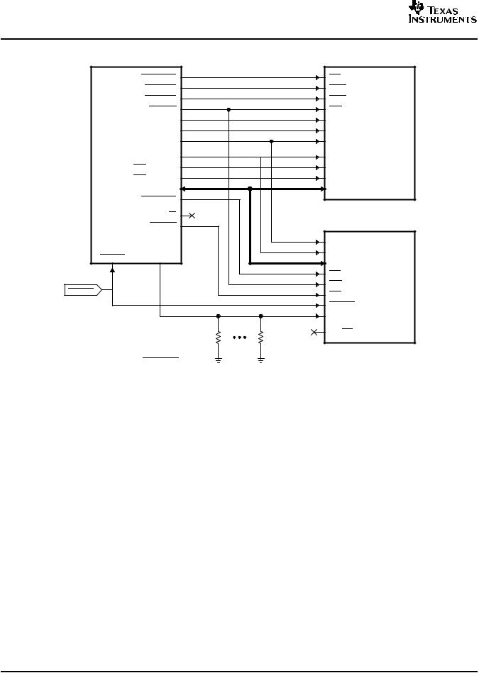
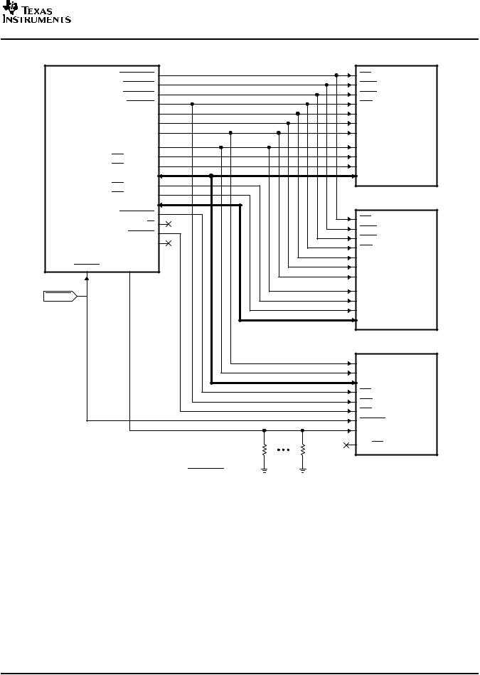
Figure 4-5 and Figure 4-6 show typical examples of EMIF-to-memory hookup on the C672x DSP.
As the figures illustrate, the C672x DSP includes a limited number of EMIF address lines. These are sufficient to connect to SDRAM seamlessly. Asynchronous memory such as FLASH typically will need to use additional GPIO pins to act as upper address lines during device boot up when the FLASH contents are copied into SDRAM. (Normally, code is executed from SDRAM since SDRAM has faster access times).
Any pins listed with a ‘Y' in the GPIO column of Table 2-12 may be used for this purpose, as long as it can be assured that they be pulled low at (and after) reset and held low until configured as outputs by the DSP.
Note that EM_BA[1:0] are used as low-order address lines for the asynchronous interface. For example, in Figure 4-5 and Figure 4-6, the flash memory is not byte-addressable and its A[0] input selects a 16-bit value. The corresponding DSP address comes from EM_BA[1]. The remaining address lines from the DSP (EM_A[12:0]) drive a word address into the flash inputs A[13:1].
For a more detailed explanation of the C672x EMIF operation please refer to the document
TMS320C672x External Memory Interface (EMIF) User's Guide (literature number SPRU711).
Submit Documentation Feedback |
Peripheral and Electrical Specifications |
45 |
TMS320C6727B, TMS320C6726B, TMS320C6722B, TMS320C6720
Floating-Point Digital Signal Processors
www.ti.com
SPRS370C–SEPTEMBER 2006–REVISED OCTOBER 2007
C6726B/C6722B/C6720 |
SDRAM |
||
DSP EMIF |
2M x 16 x 4 Bank |
||
|
EM_CS[0] |
CE |
|
|
EM_CAS |
CAS |
|
|
EM_RAS |
RAS |
|
|
EM_WE |
WE |
|
|
EM_CLK |
CLK |
|
|
EM_CKE |
CKE |
|
|
EM_BA[1:0] |
BA[1:0] |
|
|
EM_A[11:0] |
A[11:0] |
|
EM_WE_DQM[0] |
LDQM |
||
EM_WE_DQM[1] |
UDQM |
||
|
EM_D[15:0] |
DQ[15:0] |
|
|
EM_CS[2] |
|
|
|
EM_RW |
FLASH |
|
|
EM_OE |
512K x 16 |
|
|
|
||
|
|
EM_BA[1] |
|
|
GPIO |
A[0] |
|
|
A[12:1] |
||
RESET |
(6 Pins) |
||
DQ[15:0] |
|||
|
|
||
|
|
CE |
|
RESET |
|
WE |
|
|
OE |
||
|
|
||
|
|
RESET |
|
|
|
A[18:13] |
|
Any GPIO-capable pins which |
RY/BY |
||
can be pulled down at reset |
|||
|
|||
can be used to control A[18:13] |
|
||
for FLASH BOOTLOAD |
|
||
Examples: AHCLKR0, SPI0_SCS/SCL1 |
|
||
Figure 4-5. C6726B/C6722B/C6720 DSP 16-Bit EMIF Example
46 |
Peripheral and Electrical Specifications |
Submit Documentation Feedback |
TMS320C6727B, TMS320C6726B, TMS320C6722B, TMS320C6720
Floating-Point Digital Signal Processors
www.ti.com |
|
SPRS370C–SEPTEMBER 2006–REVISED OCTOBER 2007 |
|
|
|
C6727B |
SDRAM |
|
DSP EMIF |
4M x 16 x 4 Bank |
|
|
EM_CS[0] |
CE |
|
EM_CAS |
CAS |
|
EM_RAS |
RAS |
|
EM_WE |
WE |
|
EM_CLK |
CLK |
|
EM_CKE |
CKE |
|
EM_BA[1:0] |
BA[1:0] |
|
EM_A[12:0] |
A[12:0] |
EM_WE_DQM[0] |
LDQM |
|
EM_WE_DQM[1] |
UDQM |
|
|
EM_D[15:0] |
DQ[15:0] |
EM_WE_DQM[2] |
|
|
EM_WE_DQM[3] |
SDRAM |
|
EM_D[31:16]/UHPI_HA[15:0] |
4M x 16 x 4 Bank |
|
|
||
|
EM_CS[2] |
CE |
|
EM_RW |
|
|
CAS |
|
|
EM_OE |
|
|
RAS |
|
|
EM_WAIT |
|
|
WE |
|
|
|
|
|
GPIO |
CLK |
RESET |
(5 Pins) |
CKE |
|
||
|
|
BA[1:0] |
RESET |
|
A[12:0] |
|
LDQM |
|
|
|
|
|
|
UDQM |
|
|
DQ[15:0] |
|
|
FLASH |
|
|
512K x 16 |
|
|
EM_BA[1] |
|
|
A[0] |
|
|
A[13:1] |
|
|
DQ[15:0] |
|
|
CE |
|
|
WE |
|
|
OE |
|
|
RESET |
|
|
A[18:14] |
Any GPIO-capable pins which |
RY/BY |
|
can be pulled down at reset |
||
|
||
can be used to control A[18:14] |
|
|
for FLASH BOOTLOAD |
|
|
Examples: AHCLKR0, SPI0_SCS/SCL1 |
|
Figure 4-6. C6727B DSP 32-Bit EMIF Example
Submit Documentation Feedback |
Peripheral and Electrical Specifications |
47 |

TMS320C6727B, TMS320C6726B, TMS320C6722B, TMS320C6720
Floating-Point Digital Signal Processors
www.ti.com
SPRS370C–SEPTEMBER 2006–REVISED OCTOBER 2007
4.11.2 EMIF Peripheral Registers Description(s)
Table 4-4 is a list of the EMIF registers. For more information about these registers, see the
TMS320C672x DSP External Memory Interface (EMIF) User's Guide (literature number SPRU711).
|
|
Table 4-4. EMIF Registers |
BYTE ADDRESS |
REGISTER NAME |
DESCRIPTION |
0xF000 0004 |
AWCCR |
Asynchronous Wait Cycle Configuration Register |
0xF000 0008 |
SDCR |
SDRAM Configuration Register |
0xF000 000C |
SDRCR |
SDRAM Refresh Control Register |
0xF000 0010 |
A1CR |
Asynchronous 1 Configuration Register |
0xF000 0020 |
SDTIMR |
SDRAM Timing Register |
0xF000 003C |
SDSRETR |
SDRAM Self Refresh Exit Timing Register |
0xF000 0040 |
EIRR |
EMIF Interrupt Raw Register |
0xF000 0044 |
EIMR |
EMIF Interrupt Mask Register |
0xF000 0048 |
EIMSR |
EMIF Interrupt Mask Set Register |
0xF000 004C |
EIMCR |
EMIF Interrupt Mask Clear Register |
0xF000 0060 |
NANDFCR |
NAND Flash Control Register |
0xF000 0064 |
NANDFSR |
NAND Flash Status Register |
0xF000 0070 |
NANDF1ECC |
NAND Flash 1 ECC Register |
48 |
Peripheral and Electrical Specifications |
Submit Documentation Feedback |