
- •1 TMS320C6727B, TMS320C6726B, TMS320C6722B, TMS320C6720 DSPs
- •1.1 Features
- •1.2 Description
- •1.2.1 Device Compatibility
- •1.3 Functional Block Diagram
- •2 Device Overview
- •2.1 Device Characteristics
- •2.2 Enhanced C67x+ CPU
- •2.3 CPU Interrupt Assignments
- •2.4 Internal Program/Data ROM and RAM
- •2.5 Program Cache
- •2.6 High-Performance Crossbar Switch
- •2.7 Memory Map Summary
- •2.8 Boot Modes
- •2.9 Pin Assignments
- •2.9.1 Pin Maps
- •2.9.2 Terminal Functions
- •2.10 Development
- •2.10.1 Development Support
- •2.10.2 Device Support
- •3 Device Configurations
- •3.1 Device Configuration Registers
- •3.2 Peripheral Pin Multiplexing Options
- •3.3 Peripheral Pin Multiplexing Control
- •4 Peripheral and Electrical Specifications
- •4.1 Electrical Specifications
- •4.2 Absolute Maximum Ratings
- •4.3 Recommended Operating Conditions
- •4.4 Electrical Characteristics
- •4.5 Parameter Information
- •4.6 Timing Parameter Symbology
- •4.7 Power Supplies
- •4.8 Reset
- •4.8.1 Reset Electrical Data/Timing
- •4.9 Dual Data Movement Accelerator (dMAX)
- •4.9.2 dMAX Peripheral Registers Description(s)
- •4.10 External Interrupts
- •4.11 External Memory Interface (EMIF)
- •4.11.1 EMIF Device-Specific Information
- •4.11.2 EMIF Peripheral Registers Description(s)
- •4.11.3 EMIF Electrical Data/Timing
- •4.12 Universal Host-Port Interface (UHPI) [C6727B Only]
- •4.12.1 UHPI Device-Specific Information
- •4.12.2 UHPI Peripheral Registers Description(s)
- •4.12.3 UHPI Electrical Data/Timing
- •4.13 Multichannel Audio Serial Ports (McASP0, McASP1, and McASP2)
- •4.13.1 McASP Peripheral Registers Description(s)
- •4.13.2 McASP Electrical Data/Timing
- •4.14 Serial Peripheral Interface Ports (SPI0, SPI1)
- •4.14.1 SPI Device-Specific Information
- •4.14.2 SPI Peripheral Registers Description(s)
- •4.14.3 SPI Electrical Data/Timing
- •4.15 Inter-Integrated Circuit Serial Ports (I2C0, I2C1)
- •4.15.1 I2C Device-Specific Information
- •4.15.2 I2C Peripheral Registers Description(s)
- •4.15.3 I2C Electrical Data/Timing
- •4.16 Real-Time Interrupt (RTI) Timer With Digital Watchdog
- •4.16.1 RTI/Digital Watchdog Device-Specific Information
- •4.16.2 RTI/Digital Watchdog Registers Description(s)
- •4.17 External Clock Input From Oscillator or CLKIN Pin
- •4.17.1 Clock Electrical Data/Timing
- •4.18 Phase-Locked Loop (PLL)
- •4.18.1 PLL Device-Specific Information
- •4.18.2 PLL Registers Description(s)
- •5 Application Example
- •6 Revision History
- •7 Mechanical Data
- •7.1 Package Thermal Resistance Characteristics
- •7.2.1 Standoff Height
- •7.3 Packaging Information

TMS320C6727B, TMS320C6726B, TMS320C6722B, TMS320C6720
Floating-Point Digital Signal Processors
www.ti.com
SPRS370C–SEPTEMBER 2006–REVISED OCTOBER 2007
4.8 Reset
A hardware reset (RESET) is required to place the DSP into a known good state out of power-up. The RESET signal can be asserted (pulled low) prior to ramping the core and I/O voltages or after the core and I/O voltages have reached their proper operating conditions. As a best practice, RESET should be held low during power-up. Prior to deasserting RESET (low-to-high transition), the core and I/O voltages should be at their proper operating conditions.
4.8.1Reset Electrical Data/Timing
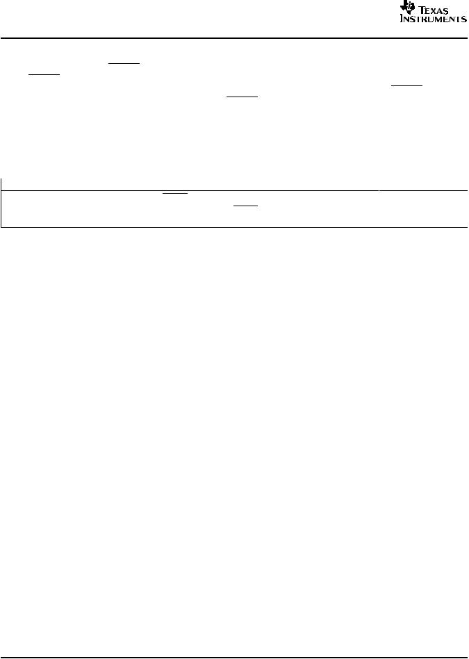
Table 4-1 assumes testing over recommended operating conditions.
Table 4-1. Reset Timing Requirements
NO. |
|
|
MIN |
MAX UNIT |
1 |
tw(RSTL) |
Pulse width, RESET low |
100 |
ns |
2 |
tsu(BPV-RSTH) |
Setup time, boot pins valid before RESET high |
20 |
ns |
3 |
th(RSTH-BPV) |
Hold time, boot pins valid after RESET high |
20 |
ns |
38 |
Peripheral and Electrical Specifications |
Submit Documentation Feedback |