- •1 Introduction
- •1.1 Features
- •1.2 Block diagram
- •2 Pin Information
- •2.1 Pin assignment
- •2.2 Pin functions
- •3 Absolute maximum ratings
- •4 Operating conditions
- •5 Electrical specifications
- •5.1 Power consumption
- •5.2 General RF conditions
- •5.3 Transmitter operation
- •5.4 Receiver operation
- •5.5 Crystal specifications
- •5.6 DC characteristics
- •5.7 Power on reset
- •6 Radio Control
- •6.1 Operational Modes
- •6.1.1 State diagram
- •6.1.2 Power Down Mode
- •6.1.3 Standby Modes
- •6.1.4 RX mode
- •6.1.5 TX mode
- •6.1.6 Operational modes configuration
- •6.1.7 Timing Information
- •6.2 Air data rate
- •6.3 RF channel frequency
- •6.4 Received Power Detector measurements
- •6.5 PA control
- •6.6 RX/TX control
- •7 Enhanced ShockBurst™
- •7.1 Features
- •7.2 Enhanced ShockBurst™ overview
- •7.3.1 Preamble
- •7.3.2 Address
- •7.3.3 Packet control field
- •7.3.3.1 Payload length
- •7.3.3.2 PID (Packet identification)
- •7.3.4 Payload
- •7.3.5 CRC (Cyclic Redundancy Check)
- •7.3.6 Automatic packet assembly
- •7.3.7 Automatic packet disassembly
- •7.4 Automatic packet transaction handling
- •7.4.1 Auto acknowledgement
- •7.4.2 Auto Retransmission (ART)
- •7.5 Enhanced ShockBurst flowcharts
- •7.5.1 PTX operation
- •7.5.2 PRX operation
- •7.8.1 Single transaction with ACK packet and interrupts
- •7.8.2 Single transaction with a lost packet
- •7.8.3 Single transaction with a lost ACK packet
- •7.8.4 Single transaction with ACK payload packet
- •7.8.5 Single transaction with ACK payload packet and lost packet
- •7.8.6 Two transactions with ACK payload packet and the first ACK packet lost
- •7.8.7 Two transactions where max retransmissions is reached
- •7.9 Compatibility with ShockBurst™
- •7.9.1 ShockBurst™ packet format
- •8 Data and Control Interface
- •8.1 Features
- •8.2 Functional description
- •8.3 SPI operation
- •8.3.1 SPI commands
- •8.3.2 SPI timing
- •8.4 Data FIFO
- •8.5 Interrupt
- •9 Register Map
- •9.1 Register map table
- •10 Peripheral RF Information
- •10.1 Antenna output
- •10.2 Crystal oscillator
- •10.3 nRF24L01+ crystal sharing with an MCU
- •10.3.1 Crystal parameters
- •10.3.2 Input crystal amplitude and current consumption
- •10.4 PCB layout and decoupling guidelines
- •11 Application example
- •11.1 PCB layout examples
- •12 Mechanical specifications
- •13 Ordering information
- •13.1 Package marking
- •13.2 Abbreviations
- •13.3 Product options
- •13.3.1 RF silicon
- •13.3.2 Development tools
- •14 Glossary of Terms
- •Appendix A - Enhanced ShockBurst™ - Configuration and communication example
- •Enhanced ShockBurst™ transmitting payload
- •Enhanced ShockBurst™ receive payload
- •Appendix B - Configuration for compatibility with nRF24XX
- •Appendix C - Constant carrier wave output for testing
- •Configuration
nRF24L01+ Product Specification
.
Legend:
Undefined |
Undefined |
|
Recommended operating mode |
|
Possible operating mode |
|
Transition state |
|
Recommended path between operating modes |
|
Possible path between operating modes |
CE = 1 |
Pin signal condition |
PWR_DN = 1 |
Bit state condition |
TX FIFO empty |
System information |
|
Undefined |
|
|
|
VDD >= 1.9V |
|
Power on |
|
|
reset |
|
|
100ms |
|
|
|
Crystal |
|
Power Down |
oscillator |
|
start up |
|
|
|
|
|
|
Tpd2stby |
|
|
PWR_UP = 1 |
PWR_UP=0 |
PWR_UP = 0 |
Standby-I |
|
||
|
|
|
PWR_UP = 0 |
|
|
|
CE = 0 |
|
PWR_UP=0
PRIM_RX = 0
TX FIFO empty
CE = 1
RX Settling
130 µs
CE = 0
RX Mode
PRIM_RX = 1 |
Standby-II |
CE = 1 |
TX FIFO not empty |
|
|
|
PRIM_RX = 0 |
|
CE = 1 for more than 10µs |
TX FIFO not empty TX finished with one packet CE = 1
CE = 0
TX Settling 130 µs
TX FIFO empty
CE = 1
PWR_UP=0
TX Mode
PWR_UP = 0
CE = 1
TX FIFO not empty
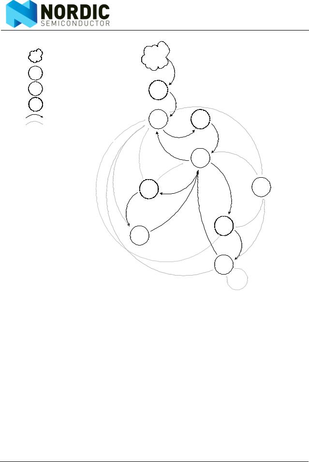
Figure 4. Radio control state diagram
6.1.2Power Down Mode
In power down mode nRF24L01+ is disabled using minimal current consumption. All register values available are maintained and the SPI is kept active, enabling change of configuration and the uploading/downloading of data registers. For start up times see Table 16. on page 24. Power down mode is entered by setting the PWR_UP bit in the CONFIG register low.
6.1.3Standby Modes
6.1.3.1Standby-I mode
By setting the PWR_UP bit in the CONFIG register to 1, the device enters standby-I mode. Standby-I mode is used to minimize average current consumption while maintaining short start up times. In this mode only part of the crystal oscillator is active. Change to active modes only happens if CE is set high and when CE is set low, the nRF24L01 returns to standby-I mode from both the TX and RX modes.
Revision 1.0 |
Page 22 of 78 |