


nRF24L01+ Product Specification
7.5Enhanced ShockBurst flowcharts
This section contains flowcharts outlining PTX and PRX operation in Enhanced ShockBurst™.
7.5.1PTX operation
The flowchart in Figure 10. outlines how a nRF24L01+ configured as a PTX behaves after entering standby-I mode.
Start Primary TX
ShockBurst operation
|
|
|
|
|
|
|
Standby-I mode |
|
|
|
|
|
|
|
|
|
No |
|
|
|
|
|
|
|
CE=1 |
|
|
|
|
|
|
|
|
Yes |
|
No |
Is CE =1? |
|
Yes |
Standby-II mode |
No |
Packet in TX |
|
|
|
FIFO? |
|
||||||
|
|
|
|
|
||||
|
|
|
|
|
|
|
Yes |
|
|
No |
|
|
|
|
|
|
|
|
|
No |
|
Packet in TX |
|
Yes |
TX Settling and |
|
|
|
|
FIFO? |
|
packet assembly |
|
||
|
|
|
|
|
|
|
||
|
Packet in TX |
|
|
Yes |
|
|
Transmit Packet |
|
|
FIFO? |
|
|
|
|
|
||
|
|
|
|
|
|
|
|
|
|
Yes |
|
|
|
|
|
Is Auto Re- |
|
|
|
|
|
Set TX_DS IRQ |
|
|
|
|
|
|
|
|
|
No |
Transmit |
|
|
|
Is CE =1? |
|
|
|
|
|
enabled? |
|
|
|
|
|
|
|
|
|
|
|
|
|
|
|
|
|
Yes |
|
|
|
|
|
|
Yes |
|
No_ACK? |
|
|
|
|
|
|
|
|
No |
|
|
|
|
|
|
|
|
RX Settling |
|
|
|
|
|
|
|
|
RX mode and |
|
|
|
|
|
|
|
|
packet |
|
|
|
|
|
|
|
|
disassembly |
|
Set MAX_RT IRQ |
|
No |
|
|
|
|
|
|
|
|
|
|
|
|
Is an ACK |
|
|
|
|
|
|
Timeout? |
|
No |
|
|
|
|
|
|
|
received? |
|
||
|
|
|
|
|
|
|
|
|
|
|
|
|
|
|
|
Yes |
|
|
|
|
|
Yes |
|
|
|
|
|
|
|
|
Standby-II mode |
|
Yes |
Has the ACK |
No |
|
|
|
|
|
payload? |
|||
|
|
|
|
|
|
|
||
|
|
No |
|
|
|
|
|
|
|
|
|
|
Has ARD |
|
|
|
|
|
|
|
|
elapsed? |
|
|
|
|
|
TX mode |
|
|
|
Put payload in RX |
|
||
|
|
|
|
|
FIFO. |
Set TX_DS IRQ |
||
Retransmit last |
|
|
Yes |
|
||||
|
|
Set TX_DS IRQ |
|
|||||
|
packet |
|
|
|
|
|||
|
|
|
|
and RX_DR IRQ |
|
|||
|
|
|
|
|
|
|||
|
TX Settling |
No |
|
Number of |
|
|
|
|
|
|
retries = ARC? |
|
|
|
|
||
|
|
|
|
|
|
|
|
|
|
Yes |
|
|
|
|
|
|
|
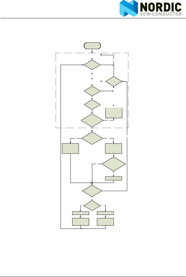
Note: ShockBurst™ operation is outlined with a dashed square.
Figure 10. PTX operations in Enhanced ShockBurst™
Revision 1.0 |
Page 35 of 78 |

nRF24L01+ Product Specification
Activate PTX mode by setting the CE pin high. If there is a packet present in the TX FIFO the nRF24L01+ enters TX mode and transmits the packet. If Auto Retransmit is enabled, the state machine checks if the NO_ACK flag is set. If it is not set, the nRF24L01+ enters RX mode to receive an ACK packet. If the received ACK packet is empty, only the TX_DS IRQ is asserted. If the ACK packet contains a payload, both TX_DS IRQ and RX_DR IRQ are asserted simultaneously before nRF24L01+ returns to standby-I mode.
If the ACK packet is not received before timeout occurs, the nRF24L01+ returns to standby-II mode. It stays in standby-II mode until the ARD has elapsed. If the number of retransmits has not reached the ARC, the nRF24L01+ enters TX mode and transmits the last packet once more.
While executing the Auto Retransmit feature, the number of defined in ARC. If this happens, the nRF24L01+ asserts the
retransmits can reach the maximum number MAX_RT IRQ and returns to standby-I mode.
If the CE is high and the TX FIFO is empty, the nRF24L01+ enters Standby-II mode.
Revision 1.0 |
Page 36 of 78 |
nRF24L01+ Product Specification
7.5.2PRX operation
The flowchart in Figure 11. outlines how a nRF24L01+ configured as a PRX behaves after entering standby-I mode.
Start Primary RX
ShockBurst operation |
Standby-I mode |
|
|
|
|
No
Is CE =1?
|
|
|
|
|
|
|
|
|
|
|
|
|
No |
|
|
|
Yes |
|
|
|
|
|
|
|
|
|
|
|
|||
|
|
|
|
|
|
|
|
|
|
|
|
||||
|
|
|
|
|
|
|
|
|
|
|
|
|
|
||
RX Settling |
|
|
|
|
|
|
|
|
|
|
|||||
|
|
|
|
|
|
|
|
|
|
|
|
Is CE =1? |
|||
RX mode |
|
|
|
||||||||||||
|
|
|
|
|
|
|
Yes |
|
|
|
|
|
|
|
|
|
|
|
|
|
|
|
|
|
|
|
|
|
|
||
|
|
|
|
|
|
|
|
|
|
|
|
|
|
|
|
|
|
|
|
|
|
|
|
|
|
|
|
|
|
|
|
RX FIFO |
|
|
|
|
|
|
|
|
|
|
|||||
|
|
|
|
|
|
|
|
|
|
||||||
|
|
|
Yes |
|
|
|
|
||||||||
Full? |
|
|
|
|
|
|
|||||||||
|
|
|
|
|
|
|
|
|
|
||||||
|
|
|
|
|
|
|
|
|
|
|
|
|
|||
|
No |
|
|
|
|
|
|
|
|
|
|
||||
Packet |
|
|
|
|
|
|
|
|
|
|
|||||
|
|
|
|
No |
|
|
|
|
|
||||||
received? |
|
|
|
|
|
|
|
|
|
||||||
|
|
|
|
|
|
|
|
|
|
||||||
|
|
|
|
|
|
|
|
|
|
||||||
|
|
|
|
|
|
|
|
|
|
Put payload in RX |
|||||
|
Yes |
|
|
|
|
|
|||||||||
|
|
|
|
|
|
|
|
FIFO and |
|||||||
|
|
|
|
|
|
|
|
|
|
|
|
||||
|
|
|
|
|
|
|
|
|
|
set RX_DR IRQ |
|||||
|
Is Auto |
|
|
Acknowledgement |
No |
|
enabled? |
|
|
Yes |
|
|
Is the received |
Yes |
No |
packet a new |
Yes |
|
packet? |
|
|
|
Put payload in RX |
Discard packet |
|
FIFO and |
|
|
set RX_DR IRQ |
|
|
Was there payload |
|
No |
attached with the last |
|
|
ACK? |
|
|
Yes |
|
|
Set TX_DS IRQ |
|
No_ACK set in |
|
|
received packet? |
|
|
No |
|
|
Pending |
|
No |
payload in TX |
Yes |
|
FIFO? |
|
TX Settling |
TX Settling |
|
TX mode Transmit ACK
TX mode Transmit ACK with payload
Note: ShockBurst™ operation is outlined with a dashed square.
Figure 11. PRX operations in Enhanced ShockBurst™
Activate PRX mode by setting the CE pin high. The nRF24L01+ enters RX mode and starts searching for packets. If a packet is received and Auto Acknowledgement is enabled, nRF24L01+ decides if the packet is new or a copy of a previously received packet. If the packet is new the payload is made available in the
Revision 1.0 |
Page 37 of 78 |

nRF24L01+ Product Specification
RX FIFO and the RX_DR IRQ is asserted. If the last received packet from the transmitter is acknowledged with an ACK packet with payload, the TX_DS IRQ indicates that the PTX received the ACK packet with payload. If the No_ACK flag is not set in the received packet, the PRX enters TX mode. If there is a pending payload in the TX FIFO it is attached to the ACK packet. After the ACK packet is transmitted, the nRF24L01+ returns to RX mode.
A copy of a previously received packet might be received if the ACK packet is lost. In this case, the PRX discards the received packet and transmits an ACK packet before it returns to RX mode.
Revision 1.0 |
Page 38 of 78 |

nRF24L01+ Product Specification
7.6MultiCeiver™
MultiCeiver™ is a feature used in RX mode that contains a set of six parallel data pipes with unique addresses. A data pipe is a logical channel in the physical RF channel. Each data pipe has its own physical address (data pipe address) decoding in the nRF24L01+.
PTX1
|
|
|
PTX3 |
|
|
PTX4 |
|
|
|
||
PTX2 |
|
|
|
|
|
|
|
|
|
|
PTX5 |
|
|
|
|
|
|
|
|
|
|
|
|
|
|
|
|
D |
4 |
|
|
|
|
|
|
|
|
|
|
t |
e |
|
|
|
|
|
|
|
|
|
|
a |
p |
|
|
|
|
|
|
|
|
|
D |
a |
|
|
|
|
|
|
|
|
|
|
P |
i |
|
|
|
|
|
|
|
|
|
|
t |
P |
|
|
|
5 |
|
|
|
|
|
|
a |
i |
a |
|
|
e |
|
|
|
|
|
|
a |
p |
|
|
|
|
|
||
|
|
|
i |
|
t |
|
|
|
|
|
|
|
|
|
e |
a |
|
|
ip |
|
|
|
|
|
|
|
P |
D |
|
|
P |
|
|
|
|
|
|
|
p |
3 |
|
ta |
|
|
|
||
|
|
|
e |
|
|
|
|
|
|
|
|
|
|
|
2 |
|
|
a |
|
|
|
|
|
|
|
|
|
|
D |
|
|
|
|
|
|
D |
|
|
|
|
|
|
|
|
|
|
|
|
|
|
|
|
|
|
|
|
|
|
|
at |
|
|
|
|
|
|
|
|
|
|
0 |
a |
Pi |
|
|
|
|
|
|
|
|
|
|
|
|
|
|
|
|
|
|
|
e |
||
|
p |
e |
|
|
|
|
|
|
|
ip |
|
|
|
|
1 |
|
|
|
|
|
ata |
|
|
|
|
|
|
|
|
|
|
D |
|
|
|
PRX
PTX6
Frequency Channel N
Figure 12. PRX using MultiCeiver™
nRF24L01+ configured as PRX (primary receiver) can receive data addressed to six different data pipes in one frequency channel as shown in Figure 12. Each data pipe has its own unique address and can be configured for individual behavior.
Up to six nRF24L01+s configured as PTX can communicate with one nRF24L01+ configured as a PRX. All data pipe addresses are searched for simultaneously. Only one data pipe can receive a packet at a time. All data pipes can perform Enhanced ShockBurst™ functionality.
The following settings are common to all data pipes:
•CRC enabled/disabled (CRC always enabled when Enhanced ShockBurst™ is enabled)
•CRC encoding scheme
•RX address width
•Frequency channel
•Air data rate
•LNA gain
The data pipes are enabled with the bits in the EN_RXADDR register. By default only data pipe 0 and 1 are enabled. Each data pipe address is configured in the RX_ADDR_PX registers.
Note: Always ensure that none of the data pipes have the same address.
Revision 1.0 |
Page 39 of 78 |
nRF24L01+ Product Specification
Each pipe can have up to a 5 byte configurable address. Data pipe 0 has a unique 5 byte address. Data pipes 1-5 share the four most significant address bytes. The LSByte must be unique for all six pipes. Figure 13. is an example of how data pipes 0-5 are addressed.
Byte 4 Byte 3 Byte 2 Byte 1 Byte 0
Data pipe 0 (RX_ADDR_P0)
Data pipe 1 (RX_ADDR_P1)
Data pipe 2 (RX_ADDR_P2)
Data pipe 3 (RX_ADDR_P3)
Data pipe 4 (RX_ADDR_P4)
Data pipe 5 (RX_ADDR_P5)
0xE7 |
0xD3 |
0xF0 |
0x35 |
0x77 |
0xC2 |
0xC2 |
0xC2 |
0xC2 |
0xC2 |
0xC2 |
0xC2 |
0xC2 |
0xC2 |
0xC3 |
0xC2 |
0xC2 |
0xC2 |
0xC2 |
0xC4 |
0xC2 |
0xC2 |
0xC2 |
0xC2 |
0xC5 |
0xC2 |
0xC2 |
0xC2 |
0xC2 |
0xC6 |
Figure 13. Addressing data pipes 0-5
Revision 1.0 |
Page 40 of 78 |
nRF24L01+ Product Specification
The PRX, using MultiCeiver™ and Enhanced ShockBurst™, receives packets from more than one PTX. To ensure that the ACK packet from the PRX is transmitted to the correct PTX, the PRX takes the data pipe address where it received the packet and uses it as the TX address when transmitting the ACK packet. Figure 14. is an example of an address configuration for the PRX and PTX. On the PRX the RX_ADDR_Pn, defined as the pipe address, must be unique. On the PTX the TX_ADDR must be the same as the RX_ADDR_P0 and as the pipe address for the designated pipe.
|
|
|
|
|
|
|
|
|
|
|
|
|
|
|
|
|
|
|
|
|
|
|
|
|
|
|
|
|
|
|
|
|
|
|
|
|
|
|
T |
|
|
|
|
|
|
||
|
|
|
|
|
|
|
|
|
|
|
|
|
|
|
|
|
|
|
|
|
|
|
|
|
|
|
|
|
|
|
|
|
|
|
|
|
R X |
|
|
|
|
|
|
||||
|
|
|
|
|
|
|
|
|
|
|
|
|
|
|
|
|
|
|
|
|
|
|
|
|
|
|
|
|
|
|
|
|
|
|
|
|
X _ |
|
|
|
|
|
|
||||
|
|
|
|
|
|
|
|
|
|
|
|
|
|
|
|
|
|
|
|
|
|
|
|
|
|
|
|
|
|
|
|
|
|
|
|
|
|
_ A |
|
|
|
|
|
||||
|
|
|
|
|
|
|
|
|
|
|
|
|
|
|
|
|
|
|
|
|
|
|
|
|
|
|
|
|
|
|
|
|
|
|
|
|
|
A D |
|
|
|
|
|
||||
|
|
|
|
|
|
|
|
|
|
|
|
|
|
|
|
|
|
|
|
|
|
|
|
|
|
|
|
|
|
|
|
|
|
|
|
|
|
|
D D |
|
|
|
|
|
|||
|
|
|
|
|
|
|
|
|
|
|
|
|
|
|
|
|
|
|
|
|
|
|
|
|
|
|
|
|
|
|
|
|
|
|
|
|
|
|
D R |
|
PTX3 |
|
|
||||
|
|
|
|
|
|
|
|
|
|
|
|
|
|
|
|
|
|
|
|
|
|
|
|
|
|
|
|
|
|
|
|
|
|
|
|
|
|
|
|
|
0 |
|
|
|
|
||
|
|
|
|
|
|
|
|
|
|
|
|
|
|
|
|
|
|
|
|
|
|
|
|
|
|
|
|
|
|
|
|
|
|
|
|
|
|
|
|
R |
: |
|
|
|
|
||
|
|
|
|
|
|
|
|
|
|
|
|
|
|
|
|
|
|
|
|
|
|
|
|
|
|
|
|
|
|
|
|
|
|
|
|
|
|
|
|
_ |
|
|
|
|
|
||
|
|
|
|
|
|
|
|
|
|
|
|
|
|
|
|
|
|
|
|
|
|
|
|
|
|
|
|
|
|
|
|
|
|
|
|
|
|
|
|
|
P |
|
|
|
|
|
|
|
|
|
|
|
|
|
|
|
|
|
|
|
|
|
|
|
|
|
|
|
|
|
|
|
|
|
|
|
|
|
|
|
|
|
|
|
|
|
|
|
: 0 |
|
|
|
|||
|
|
|
|
|
|
|
|
|
|
|
|
|
|
|
|
|
|
|
|
|
|
|
|
|
|
|
|
|
|
|
|
|
|
|
|
|
|
|
|
|
|
0 x |
|
|
|||
|
|
|
|
|
|
|
|
|
|
|
|
|
|
|
|
|
|
|
|
|
|
|
|
|
|
|
|
|
|
|
|
|
|
|
|
|
|
|
|
|
|
x B |
|
|
|||
|
|
|
|
|
|
|
|
|
|
|
|
|
|
|
|
|
|
|
|
|
|
|
|
|
|
|
|
|
|
|
|
|
|
|
|
|
|
|
|
|
|
B 3 |
|
|
|||
|
|
|
|
|
|
|
|
|
|
|
|
|
|
|
|
|
|
|
|
|
|
|
|
|
|
|
|
PTX2 |
|
|
|
|
|
3B |
|
|
|||||||||||
|
|
|
|
|
|
|
|
|
|
|
|
|
|
|
|
|
|
|
|
|
|
|
|
|
|
|
|
|
|
|
|
|
|
5 B |
|
|
|||||||||||
|
|
|
|
|
|
|
|
|
|
|
|
|
|
|
|
|
|
|
|
|
|
|
|
|
|
|
|
|
|
|
|
|
|
|
|
|
|
|
|
|
|
|
B |
4 |
|
|
|
|
|
|
|
|
|
|
|
|
|
|
|
|
|
|
|
|
|
|
|
|
|
|
|
|
|
|
|
|
|
|
|
|
|
|
|
|
|
|
|
|
|
|
4 B |
|
|
||
|
|
|
|
|
|
|
|
|
|
T |
|
|
|
|
|
|
|
|
|
|
|
|
|
|
|
|
|
|
|
|
|
|
|
|
|
|
|
|
|
|
|
|
B 5 |
|
|
||
|
|
|
|
|
|
|
|
|
|
|
|
|
|
|
|
|
|
|
|
|
|
|
|
|
|
|
|
|
|
|
|
|
|
|
|
|
|
|
|
|
|
|
6 A |
|
|
||
|
|
|
|
|
|
|
|
|
|
|
X |
_ |
|
|
|
|
|
|
|
|
|
|
|
|
|
|
|
|
|
|
|
|
|
|
|
|
|
|
|
|
|
|
|
|
|||
|
|
|
|
|
|
|
|
|
R |
|
|
|
|
A |
D |
|
|
|
|
|
|
|
|
|
|
|
|
|
|
|
|
|
|
|
|
|
|
|
|
|
|
B 6 |
|
|
|||
|
|
|
|
|
|
|
|
|
X |
|
|
|
D |
R: |
|
|
|
|
|
|
|
|
|
|
|
|
|
|
|
|
|
|
|
|
|
|
A 3 |
|
|
||||||||
|
|
|
|
|
|
|
|
|
_A |
|
|
|
|
|
|
|
|
|
|
|
|
|
|
|
|
|
|
|
|
|
|
|
3 |
|
|
||||||||||||
|
|
|
|
|
|
|
|
|
|
|
D |
|
|
|
|
|
|
|
|
|
|
|
|
|
|
|
|
|
|
|
|
|
|
|
|
|
|
||||||||||
|
|
|
|
|
|
|
|
|
|
|
|
|
|
|
|
|
|
|
|
|
|
|
|
|
|
|
|
|
|
|
|
|
|
|
|
|
|
|
|
|
|||||||
|
|
|
|
|
|
|
|
|
|
|
|
|
|
|
|
D |
|
|
|
|
|
|
|
|
|
|
|
|
|
|
|
|
|
|
|
|
|
|
|
|
|
|
|
|
|
||
|
|
|
|
|
|
|
|
|
|
|
|
|
|
|
|
|
|
R |
|
|
|
|
|
|
0 |
|
|
|
|
|
|
|
|
|
|
|
|
|
|
|
|
|
D |
4 |
|||
|
|
|
|
|
|
|
|
|
|
|
|
|
|
|
|
|
|
|
|
_ |
P |
0 |
: |
|
x |
B |
3 |
B |
|
|
|
|
|
|
|
|
|
|
|
|
|||||||
|
|
|
|
|
|
|
|
|
|
|
|
|
|
|
|
|
|
|
|
|
|
|
0 |
x |
|
4 |
B |
|
|
|
|
|
|
|
|
|
|
a |
e |
||||||||
|
|
|
|
|
|
|
|
|
|
|
|
|
|
|
|
|
|
|
|
|
|
|
|
|
|
|
|
|
|
|
|
|
|
|
|
|
|
t |
|||||||||
|
|
|
|
|
|
|
|
|
|
|
|
|
|
|
|
|
|
|
|
|
|
|
|
|
|
|
|
|
B |
3 |
B4 |
|
5 |
B6 |
|
|
|
|
|
|
D |
a |
p |
||||
|
|
|
|
|
|
|
|
|
|
|
|
|
|
|
|
|
|
|
|
|
|
|
|
|
|
|
|
|
|
|
|
B |
|
|
C |
|
|
|
|
|
i |
||||||
|
|
|
|
|
|
|
|
|
|
|
|
|
|
|
|
|
|
|
|
|
|
|
|
|
|
|
|
|
|
|
|
|
|
5 |
|
|
|
|
|
|
|
a |
P |
P |
|||
|
|
|
|
|
|
|
|
|
|
|
|
|
|
|
|
|
|
|
|
|
|
|
|
|
|
|
|
|
|
|
|
|
|
|
B6 |
C |
|
D |
|
|
|
||||||
|
|
|
|
|
|
|
|
|
|
|
|
|
|
|
|
|
|
|
|
|
|
|
|
|
|
|
|
|
|
|
|
|
|
|
|
D |
|
|
|
|
t |
i |
a |
||||
|
|
|
|
|
|
|
|
|
|
|
|
|
|
|
|
|
|
|
|
|
|
|
|
|
|
|
|
|
|
|
|
|
|
|
|
|
|
|
|
|
|
a |
p |
||||
|
|
|
|
|
|
|
|
|
|
PTX1 |
|
|
|
|
|
|
|
|
|
|
|
|
|
|
|
|
|
|
|
|
e |
3 |
t |
||||||||||||||
|
|
|
|
|
|
|
|
|
|
|
|
|
|
|
|
|
|
|
|
|
|
|
|
|
|
|
|
|
|
|
|
D |
|||||||||||||||
|
|
|
|
|
|
|
|
|
|
|
|
|
|
|
|
|
|
|
|
|
|
|
|
|
|
|
|
|
|
|
|
|
|
|
|
|
|
|
|
|
|
|
|
|
P |
e |
a |
|
|
|
|
|
|
|
|
|
|
|
|
|
|
|
|
|
|
|
|
|
|
|
|
|
|
|
|
|
|
|
|
|
|
|
|
|
|
|
|
|
|
|
|
|
i |
|
|
|
|
|
|
|
|
|
|
|
|
|
|
|
|
|
|
|
|
|
|
|
|
|
|
|
|
|
|
|
|
|
|
|
|
|
|
|
|
|
|
|
|
|
|
|
p |
|
|
X |
|
|
|
|
|
|
|
|
|
|
|
|
|
|
|
|
|
|
|
|
|
|
|
|
|
|
|
|
|
|
|
|
|
|
|
|
D |
|
|
|
|
|
2 |
|
|
||
|
|
|
|
|
|
|
|
|
|
|
|
|
|
|
|
|
|
|
|
|
|
|
|
|
|
|
|
|
|
|
|
|
|
|
|
|
|
|
|
|
|
|
|
||||
T |
|
_ |
A |
|
|
|
|
|
|
|
|
|
|
|
|
|
|
|
|
|
|
|
|
|
|
|
|
|
|
|
|
|
|
|
|
|
|
|
a |
|
|
|
|
|
|
|
|
RX |
|
|
|
|
DD |
R |
|
|
|
|
|
|
|
|
|
|
|
|
|
|
|
|
|
|
|
|
|
|
|
|
|
|
|
|
|
|
|
a |
Pi |
|
|
|
|
||||
_A |
|
|
|
|
|
: |
|
|
|
|
|
|
|
|
|
|
|
|
|
|
|
|
|
|
|
|
|
|
|
|
|
|
|
|
|
|
|
|
|
|
|
||||||
|
D |
|
|
|
|
|
|
|
|
|
|
|
|
|
|
|
|
|
|
|
|
|
|
|
|
|
|
|
|
|
|
|
|
|
|
|
|
|
p |
|
|
|
|||||
|
|
|
|
D |
R |
_ |
P |
|
|
|
0 |
xB |
3 |
B |
4 |
|
|
|
|
|
|
|
|
|
|
|
|
|
|
|
|
|
|
|
e |
1 |
|
|
|||||||||
|
|
|
|
|
|
|
|
|
|
|
|
|
|
|
|
|
|
|
|
|
|
|
|
|
|
|
|
|
|
|
|||||||||||||||||
|
|
|
|
|
|
|
|
|
|
|
|
|
|
|
|
|
|
|
|
|
|
|
|
|
|
|
|
|
|
|
|
|
|
|
|
|
|
|
|
||||||||
|
|
|
|
|
|
|
|
|
|
|
0 |
: |
|
|
|
|
|
|
|
|
|
|
|
|
|
|
|
|
|
|
|
|
|
|
|
|
|
|
|
|
|
|
|
|
|||
|
|
|
|
|
|
|
|
|
|
|
|
0 |
|
|
|
|
|
|
|
|
B |
5 |
B |
|
|
|
|
|
|
|
|
|
|
|
|
|
|
|
|
|
|
||||||
|
|
|
|
|
|
|
|
|
|
|
|
|
|
|
x |
B |
3 |
|
|
|
|
|
|
|
6 |
|
|
|
|
|
|
|
|
|
|
|
|
|
|
|
|
||||||
|
|
|
|
|
|
|
|
|
|
|
|
|
|
|
|
|
|
|
B |
|
|
|
|
|
|
|
|
F |
1 |
|
|
|
|
|
|
|
|
|
|
|
|
|
|
||||
|
|
|
|
|
|
|
|
|
|
|
|
|
|
|
|
|
|
|
|
|
|
4B |
|
|
|
|
|
|
|
|
|
|
|
|
|
|
|
|
|
|
|
|
|
|
|
||
|
|
|
|
|
|
|
|
|
|
|
|
|
|
|
|
|
|
|
|
|
|
|
|
5B |
|
|
F1 |
|
|
|
|
|
|
|
|
|
|
|
|
|
|
||||||
|
|
|
|
|
|
|
|
|
|
|
|
|
|
|
|
|
|
|
|
|
|
|
|
|
|
|
|
6 |
|
|
|
|
|
|
|
|
|
|
|
|
|
|
|||||
|
|
|
|
|
|
|
|
|
|
|
|
|
|
|
|
|
|
|
|
|
|
|
|
|
|
|
|
|
|
|
|
|
|
|
|
|
|
|
|
|
|
|
|
|
|||
PRX
PTX4
|
|
|
|
|
D |
R |
: |
|
R |
|
|
|
|
D |
|
D |
|||
|
|
X _ |
A |
|
D |
||||
|
|
|
A |
|
|||||
|
T |
|
_ |
|
|
||||
|
R |
X |
|
|
|
||||
|
|
|
|
|
|
||||
|
|
|
|
|
|
|
|
|
|
|
|
|
|
|
|
e |
5 |
||
|
|
|
|
|
|
|
|
||
|
|
|
|
ip |
|
|
|
||
|
ta |
P |
|
|
|
|
|
||
|
|
|
|
|
|
|
|
||
a |
|
|
|
|
|
|
|
|
|
D |
|
|
|
|
|
|
|
|
|
|
|
|
|
|
|
|
|
B |
6 |
0 |
F |
|
0 |
F |
|
|
|
|
|
|
|
|
|
|
|
|
|
|
|
|
5 |
B |
6 |
|
|
|
|
|
|
|
|
|
|||||
|
|
|
|
|
|
B |
5 |
|
|
|
|
|
|
|
|
|
|
||||||
|
|
|
|
|
4 |
B |
|
|
|
|
|
|
|
|
|
|
|
||||||
|
|
|
3 |
B |
|
4 |
|
|
|
|
|
|
|
|
|
|
|
|
|||||
|
|
B |
|
B |
|
|
|
|
|
|
|
|
|
|
|
|
|
|
|||||
|
x |
|
3 |
|
|
|
|
|
|
|
|
|
|
|
|
|
|
|
|||||
0 |
|
B |
|
|
|
|
|
|
|
|
|
|
|
|
|
|
|
|
|||||
|
x |
|
|
|
|
|
|
|
|
|
|
|
|
|
|
|
|
|
|||||
|
0 |
|
|
|
|
|
|
|
|
|
|
|
|
|
|
|
|
|
|
||||
|
: |
|
|
|
|
|
|
|
|
|
|
|
|
|
|
|
|
|
|
|
|||
|
0 |
|
|
|
|
|
|
|
|
|
PTX5 |
|
|
|
|
|
|
||||||
_ P |
|
|
|
|
|
|
|
|
|
|
|
|
|
|
|
|
|||||||
|
|
|
|
|
|
|
|
|
|
|
|
|
|
|
|
|
|||||||
|
|
|
|
|
|
|
|
|
|
|
|
|
|
|
|
5 |
|||||||
|
|
|
|
|
|
|
|
|
|
|
|
|
|
|
|
|
|
|
|
|
|
||
|
|
|
|
|
|
|
|
|
|
|
|
|
|
|
|
|
|
|
|
|
|
0 |
|
|
|
|
|
|
|
|
|
|
|
|
|
|
|
|
|
|
|
|
|
|
6 |
5 |
|
|
|
|
|
|
|
|
|
|
|
|
|
|
|
|
|
|
|
|
|
|
B |
|
|
|
|
|
|
|
|
|
|
|
|
|
|
|
|
|
|
|
|
|
|
5 |
0 |
||
|
|
|
|
|
|
|
|
|
|
|
|
|
|
|
|
|
|
|
|
B |
|
6 |
|
|
|
|
|
|
|
|
|
|
|
|
|
|
|
|
|
|
|
|
|
4 |
B |
|
|
|
|
|
|
|
|
|
|
|
|
|
|
|
|
|
|
|
|
|
B |
5 |
|
||
|
|
|
|
|
|
|
|
|
|
|
|
|
|
|
|
|
|
3 |
B |
|
|
||
|
|
|
|
|
|
|
|
|
|
|
|
|
|
|
|
|
|
B |
|
4 |
|
|
|
|
|
|
|
|
|
|
|
|
|
|
|
|
|
|
|
|
x |
|
B |
|
|
|
|
|
|
|
|
|
|
|
|
|
|
|
|
|
|
|
|
|
0 |
|
3 |
|
|
|
|
|
|
|
|
|
|
|
|
|
|
|
|
|
|
|
|
|
|
B |
|
|
|
||
|
|
|
|
|
|
|
|
|
|
|
|
|
|
|
|
|
|
x |
|
|
|
|
|
|
|
|
|
|
|
|
|
|
|
|
|
|
|
|
: |
0 |
|
|
|
|
|
||
|
|
|
|
|
|
|
|
|
|
|
|
|
|
|
: |
|
|
|
|
|
|||
|
|
|
|
|
|
|
|
|
|
|
|
|
|
|
R |
|
0 |
|
|
|
|
|
|
|
|
|
|
|
|
|
|
|
|
|
|
|
|
|
D |
|
P |
|
|
|
|
|
|
|
|
|
|
|
|
|
|
|
|
|
|
|
|
D |
_ |
|
|
|
|
|
|
||
|
|
|
|
|
|
|
|
|
|
|
|
A |
R |
|
|
|
|
|
|
|
|||
|
|
|
|
|
|
|
|
|
|
|
_ |
|
D |
|
|
|
|
|
|
|
|
||
|
|
|
|
|
|
|
|
|
|
X |
|
|
|
D |
|
|
|
|
|
|
|
|
|
|
|
|
|
|
|
|
|
T |
|
|
|
A |
|
|
|
|
|
|
|
|
|||
|
|
|
|
|
|
|
|
|
|
|
|
|
_ |
|
|
|
|
PTX6 |
|||||
|
|
|
|
|
|
|
|
|
|
|
X |
|
|
|
|
|
|||||||
|
|
|
|
|
|
|
|
|
|
R |
|
|
|
|
|
|
|
|
|
|
|||
|
|
|
|
|
0 |
|
|
|
|
|
|
|
|
|
|
|
|
|
|
|
|
|
|
|
|
|
|
|
|
|
|
e |
|
|
|
|
|
|
|
|
|
|
|
|
|
|
|
|
|
|
|
7 |
|
||
|
|
|
ip |
|
|
|
|
|
|
|
|
|
|
|
|
|
|
|
|
|
|
|
|
|
|||
|
|
P |
|
|
|
|
|
|
|
|
|
|
|
|
|
|
|
|
|
|
8 |
8 |
8 |
||||
|
ta |
|
|
|
|
|
|
|
|
|
|
|
|
|
|
|
|
|
|
|
|
|
|
|
|||
a |
|
|
|
|
|
|
|
|
|
|
|
|
|
|
|
|
|
7 |
7 |
7 |
8 |
8 |
|||||
D |
|
|
|
|
|
|
|
|
|
|
|
|
|
|
|
|
|
|
|
|
|
|
|
||||
|
|
|
|
|
|
|
|
|
|
|
|
|
|
|
|
|
|
8 |
8 |
|
|
7 |
7 |
||||
|
|
|
|
|
|
|
|
|
|
|
|
|
|
|
|
|
7 |
|
|
|
|
8 |
|
|
|
||
|
|
|
|
|
|
|
|
|
|
|
|
|
|
|
|
x |
|
|
|
|
7 |
|
|
|
|
||
|
|
|
|
|
|
|
|
|
|
|
|
|
|
|
0 |
|
|
|
|
8 |
|
|
|
|
|
||
|
|
|
|
|
|
|
|
|
|
|
|
|
|
|
|
|
|
|
|
7 |
|
|
|
|
|
|
|
|
|
|
|
|
|
|
|
|
|
|
|
|
|
|
|
|
|
|
8 |
|
|
|
|
|
|
|
|
|
|
|
|
|
|
|
|
|
|
|
: |
|
|
|
|
|
7 |
|
|
|
|
|
|
|
|
||
|
|
|
|
|
|
|
|
|
|
|
|
|
|
|
x |
|
|
|
|
|
|
|
|
|
|||
|
|
|
|
|
|
|
|
|
|
R |
|
|
|
|
0 |
|
|
|
|
|
|
|
|
|
|
||
|
|
|
|
|
|
|
|
|
D |
|
|
|
|
: |
|
|
|
|
|
|
|
|
|
|
|
||
|
|
|
|
|
|
|
|
D |
|
|
|
|
0 |
|
|
|
|
|
|
|
|
|
|
|
|
||
|
|
|
|
|
|
|
A |
|
|
|
|
P |
|
|
|
|
|
|
|
|
|
|
|
|
|
||
|
|
|
|
|
|
_ |
|
|
|
|
_ |
|
|
|
|
|
|
|
|
|
|
|
|
|
|
||
|
|
|
|
|
X |
|
|
|
|
R |
|
|
|
|
|
|
|
|
|
|
|
|
|
|
|
||
|
|
|
|
|
T |
|
|
|
|
D |
|
|
|
|
|
|
|
|
|
|
|
|
|
|
|
|
|
|
|
|
|
|
|
|
|
|
D |
|
|
|
|
|
|
|
|
|
|
|
|
|
|
|
|
|
|
|
|
|
|
|
|
|
|
A |
|
|
|
|
|
|
|
|
|
|
|
|
|
|
|
|
|
|
|
|
|
|
|
|
|
|
_ |
|
|
|
|
|
|
|
|
|
|
|
|
|
|
|
|
|
|
|
|
|
|
|
|
|
|
X |
|
|
|
|
|
|
|
|
|
|
|
|
|
|
|
|
|
|
|
|
|
|
|
|
|
|
R |
|
|
|
|
|
|
|
|
|
|
|
|
|
|
|
|
|
|
|
|
|
|
Addr Data Pipe 0 (RX_ADDR_P0): 0x7878787878
Addr Data Pipe 1 (RX_ADDR_P1): 0xB3B4B5B6F1
Addr Data Pipe 2 (RX_ADDR_P2): 0xB3B4B5B6CD
Addr Data Pipe 3 (RX_ADDR_P3): 0xB3B4B5B6A3
Addr Data Pipe 4 (RX_ADDR_P4): 0xB3B4B5B60F
Addr Data Pipe 5 (RX_ADDR_P5): 0xB3B4B5B605
Frequency Channel N
Figure 14. Example of data pipe addressing in MultiCeiver™
Only when a data pipe receives a complete packet can other data pipes begin to receive data. When multiple PTXs are transmitting to a PRX, the ARD can be used to skew the auto retransmission so that they only block each other once.
Revision 1.0 |
Page 41 of 78 |

nRF24L01+ Product Specification
7.7Enhanced ShockBurst™ timing
This section describes the timing sequence of Enhanced ShockBurst™ and how all modes are initiated and operated. The Enhanced ShockBurst™ timing is controlled through the Data and Control interface. The nRF24L01+ can be set to static modes or autonomous modes where the internal state machine controls the events. Each autonomous mode/sequence ends with an interrupt at the IRQ pin. All the interrupts are indicated as IRQ events in the timing diagrams.
>10us
|
|
|
|
TIRQ |
|
TUL |
Tstdby2a |
TOA |
|
PTX SPI |
UL |
|
|
IRQ: |
|
|
TX DS1 |
||
PTX CE |
|
|
|
|
PTX IRQ |
|
|
|
|
PTX MODE |
Standby-I |
PLL Lock |
TX |
Standby-I |
1 IRQ if No Ack is on.
TIRQ = 8.2µs @ 1Mbps, TIRQ = 6.0µs @ 2Mbps, Tstdby2a = 130us
Figure 15. Transmitting one packet with NO_ACK on
The following equations calculate various timing measurements:
Symbol |
Description |
|
|
|
|
|
|
|
|
|
|
Equation |
|
|
|
|
|
|
|
|
TOA |
Time on-air |
|
|
|
|
|
|
|
|
|
|
|
|
|
|
|
|
|
|
|
|
|
|
|
|
|
|
|
|
|
|
|
|
|
|
|
+ |
9[bit] |
|||
|
|
|
|
packet length |
|
8 bit byte |
1[byte]+3,4or 5[bytes]+ N [bytes ]+1or 2[bytes] |
|||||||||||||
|
|
|
|
|
|
|
|
|
preamble |
address |
payload |
|
CRC |
|
|
packet control field |
||||
|
|
TOA = |
|
|
|
= |
|
|
|
|
|
|
|
|
[bit s |
] |
|
|
|
|
|
|
|
air data rate |
|
|
|
|
|
|
air data rate |
|
|
|
|
||||||
|
|
|
|
|
|
|
|
|
|
|
|
|
|
|
|
|
|
|
|
|
TACK |
Time on-air Ack |
|
|
|
|
|
|
|
|
|
|
|
|
|
|
|
|
|
|
|
|
|
|
|
|
|
|
|
8 bit |
|
|
|
|
|
|
|
|
+ |
9[bit] |
||
|
|
|
|
packet length |
|
|
1[byte]+ 3,4 or 5[bytes]+ N [bytes ]+1or 2[bytes] |
|||||||||||||
|
|
|
|
|
|
|
|
byte |
preamble |
address |
payload |
|
CRC |
|
|
packet control field |
||||
|
|
TACK = |
|
= |
|
|
|
|
|
|
|
|
[bit s |
] |
|
|
|
|
||
|
|
air data rate |
|
|
|
|
|
|
air data rate |
|
|
|
|
|||||||
|
|
|
|
|
|
|
|
|
|
|
|
|
|
|
|
|
|
|
|
|
TUL |
Time Upload |
|
|
|
|
|
|
|
|
|
|
|
|
|
|
|
|
|
|
|
|
|
|
|
payload length |
8 bit byte N [bytes] |
|
|
|
|
|
|
|
||||||||
|
|
|
|
|
|
payload |
|
|
|
|
|
|
|
|||||||
|
|
TUL = |
|
|
= |
SPI data rate [bit s ] |
|
|
|
|
|
|
|
|||||||
|
|
SPI data rate |
|
|
|
|
|
|
|
|
||||||||||
|
|
|
|
|
|
|
|
|
|
|
|
|
|
|
|
|||||
TESB |
Time Enhanced Shock- |
TESB = TUL + 2 . Tstby2a + TOA + TACK + TIRQ |
|
|
|
|
|
|
||||||||||||
|
Burst™ cycle |
|
|
|
|
|
|
|
|
|
|
|
|
|
|
|
|
|
|
|
|
|
|
|
Table 19. Timing equations |
|
|
|
|
|
|
|
|||||||||
Revision 1.0 |
Page 42 of 78 |

nRF24L01+ Product Specification
TESB Cycle
>10us
|
TUL |
130us |
TOA |
|
TIRQ |
|
|
|
|
|
|
|
|||
PTX SPI |
UL |
|
|
|
|
IRQ: |
|
|
|
|
|
TX DS |
|
||
|
|
|
|
|
|
|
|
PTX CE |
|
|
|
|
|
|
|
PTX IRQ |
|
|
|
|
|
|
|
PTX MODE |
Standby 1 |
PLL Lock |
TX |
PLL Lock |
RX |
Standby 1 |
|
PRX MODE |
Standby 1 |
PLL Lock |
RX |
PLL Lock |
TX |
PLL Lock |
RX |
PRX IRQ |
|
|
|
|
|
|
|
PRX CE |
|
|
|
|
|
|
|
PRX SPI |
|
|
|
IRQ:RX DR/DL |
|
|
|
|
|
130us |
|
130us |
TACK |
130us |
|
|
|
|
|
TIRQ |
|
|
|
Figure 16. Timing of Enhanced ShockBurst™ for one packet upload (2Mbps)
In Figure 16. the transmission and acknowledgement of a packet is shown. The PRX device activates RX mode (CE=1), and the PTX device is activated in TX mode (CE=1 for minimum 10µs). After 130µs the transmission starts and finishes after the elapse of TOA.
When the transmission ends the PTX device automatically switches to RX mode to wait for the ACK packet from the PRX device. When the PRX device receives the packet it sets the interrupt for the host MCU and switches to TX mode to send an ACK. After the PTX device receives the ACK packet it sets the interrupt to the MCU and clears the packet from the TX FIFO.
Revision 1.0 |
Page 43 of 78 |

nRF24L01+ Product Specification
In Figure 17. the PTX timing of a packet transmission is shown when the first ACK packet is lost. To see the complete transmission when the ACK packet fails see Figure 20. on page 46.
|
|
>10us |
|
|
|
ARD |
|
|
|
|
|
|
|
|
|
|
|
|
TUL |
130us |
TOA |
130us |
250us |
|
130us |
|
|
max |
|
|
|||||
|
|
|
|
|
|
|
|
|
PTX SPI |
UL |
|
|
|
|
|
|
|
PTX CE |
|
|
|
|
|
|
|
|
PTX IRQ |
|
|
|
|
|
|
|
|
PTX MODE |
Standby I |
PLL Lock |
TX |
PLL Lock |
RX |
Standby II |
PLL Lock |
TX |
Figure 17. Timing of Enhanced ShockBurst™ when the first ACK packet is lost (2Mbps)
Revision 1.0 |
Page 44 of 78 |