- •1 Introduction
- •1.1 Features
- •1.2 Block diagram
- •2 Pin Information
- •2.1 Pin assignment
- •2.2 Pin functions
- •3 Absolute maximum ratings
- •4 Operating conditions
- •5 Electrical specifications
- •5.1 Power consumption
- •5.2 General RF conditions
- •5.3 Transmitter operation
- •5.4 Receiver operation
- •5.5 Crystal specifications
- •5.6 DC characteristics
- •5.7 Power on reset
- •6 Radio Control
- •6.1 Operational Modes
- •6.1.1 State diagram
- •6.1.2 Power Down Mode
- •6.1.3 Standby Modes
- •6.1.4 RX mode
- •6.1.5 TX mode
- •6.1.6 Operational modes configuration
- •6.1.7 Timing Information
- •6.2 Air data rate
- •6.3 RF channel frequency
- •6.4 Received Power Detector measurements
- •6.5 PA control
- •6.6 RX/TX control
- •7 Enhanced ShockBurst™
- •7.1 Features
- •7.2 Enhanced ShockBurst™ overview
- •7.3.1 Preamble
- •7.3.2 Address
- •7.3.3 Packet control field
- •7.3.3.1 Payload length
- •7.3.3.2 PID (Packet identification)
- •7.3.4 Payload
- •7.3.5 CRC (Cyclic Redundancy Check)
- •7.3.6 Automatic packet assembly
- •7.3.7 Automatic packet disassembly
- •7.4 Automatic packet transaction handling
- •7.4.1 Auto acknowledgement
- •7.4.2 Auto Retransmission (ART)
- •7.5 Enhanced ShockBurst flowcharts
- •7.5.1 PTX operation
- •7.5.2 PRX operation
- •7.8.1 Single transaction with ACK packet and interrupts
- •7.8.2 Single transaction with a lost packet
- •7.8.3 Single transaction with a lost ACK packet
- •7.8.4 Single transaction with ACK payload packet
- •7.8.5 Single transaction with ACK payload packet and lost packet
- •7.8.6 Two transactions with ACK payload packet and the first ACK packet lost
- •7.8.7 Two transactions where max retransmissions is reached
- •7.9 Compatibility with ShockBurst™
- •7.9.1 ShockBurst™ packet format
- •8 Data and Control Interface
- •8.1 Features
- •8.2 Functional description
- •8.3 SPI operation
- •8.3.1 SPI commands
- •8.3.2 SPI timing
- •8.4 Data FIFO
- •8.5 Interrupt
- •9 Register Map
- •9.1 Register map table
- •10 Peripheral RF Information
- •10.1 Antenna output
- •10.2 Crystal oscillator
- •10.3 nRF24L01+ crystal sharing with an MCU
- •10.3.1 Crystal parameters
- •10.3.2 Input crystal amplitude and current consumption
- •10.4 PCB layout and decoupling guidelines
- •11 Application example
- •11.1 PCB layout examples
- •12 Mechanical specifications
- •13 Ordering information
- •13.1 Package marking
- •13.2 Abbreviations
- •13.3 Product options
- •13.3.1 RF silicon
- •13.3.2 Development tools
- •14 Glossary of Terms
- •Appendix A - Enhanced ShockBurst™ - Configuration and communication example
- •Enhanced ShockBurst™ transmitting payload
- •Enhanced ShockBurst™ receive payload
- •Appendix B - Configuration for compatibility with nRF24XX
- •Appendix C - Constant carrier wave output for testing
- •Configuration

nRF24L01+ Product Specification
2 Pin Information
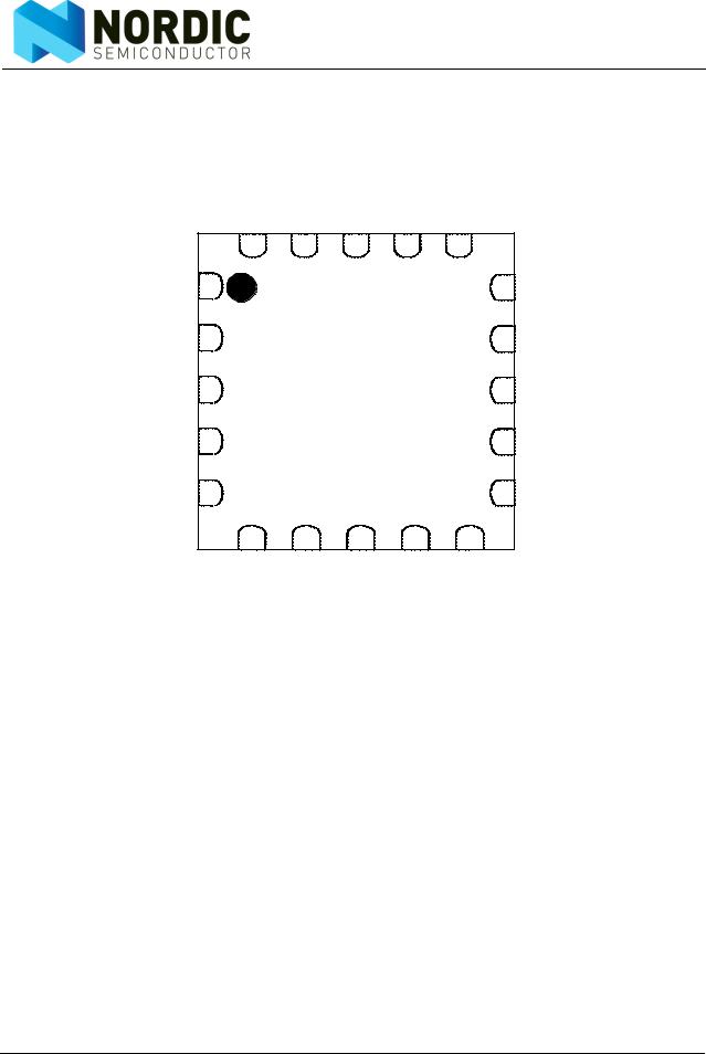
2.1Pin assignment
|
VSS |
DVDD |
VDD |
VSS |
IREF |
|
|
20 |
19 |
18 |
17 |
16 |
|
CE |
1 |
|
|
|
15 |
VDD |
|
|
|
|
|||
CSN |
2 |
|
|
|
14 |
VSS |
|
|
|
|
|
|
|
SCK |
3 |
nRF24L01+ |
13 |
ANT2 |
||
|
|
|
||||
|
|
|
QFN20 4X4 |
|
|
|
MOSI |
4 |
|
|
|
12 |
ANT1 |
MISO |
5 |
|
|
|
11 |
VDD_PA |
|
6 |
7 |
8 |
9 |
10 |
|
|
IRQ |
VDD |
VSS |
XC2 |
XC1 |
|
Figure 2. nRF24L01+ pin assignment (top view) for the QFN20 4x4 package
Revision 1.0 |
Page 10 of 78 |

nRF24L01+ Product Specification
2.2Pin functions
Pin |
Name |
Pin function |
Description |
1 |
CE |
Digital Input |
Chip Enable Activates RX or TX mode |
2 |
CSN |
Digital Input |
SPI Chip Select |
3 |
SCK |
Digital Input |
SPI Clock |
4 |
MOSI |
Digital Input |
SPI Slave Data Input |
5 |
MISO |
Digital Output |
SPI Slave Data Output, with tri-state option |
6 |
IRQ |
Digital Output |
Maskable interrupt pin. Active low |
7 |
VDD |
Power |
Power Supply (+1.9V - +3.6V DC) |
8 |
VSS |
Power |
Ground (0V) |
9 |
XC2 |
Analog Output |
Crystal Pin 2 |
10 |
XC1 |
Analog Input |
Crystal Pin 1 |
11 |
VDD_PA |
Power Output |
Power Supply Output (+1.8V) for the internal |
|
|
|
nRF24L01+ Power Amplifier. Must be connected |
|
|
|
to ANT1 and ANT2 as shown in Figure 32. |
12 |
ANT1 |
RF |
Antenna interface 1 |
13 |
ANT2 |
RF |
Antenna interface 2 |
14 |
VSS |
Power |
Ground (0V) |
15 |
VDD |
Power |
Power Supply (+1.9V - +3.6V DC) |
16 |
IREF |
Analog Input |
Reference current. Connect a 22kΩ resistor to |
|
|
|
ground. See Figure 32. |
17 |
VSS |
Power |
Ground (0V) |
18 |
VDD |
Power |
Power Supply (+1.9V - +3.6V DC) |
19 |
DVDD |
Power Output |
Internal digital supply output for de-coupling pur- |
|
|
|
poses. See Figure 32. |
20 |
VSS |
Power |
Ground (0V) |
Table 1. nRF24L01+ pin function
Revision 1.0 |
Page 11 of 78 |
