

Добавил:
Upload
Опубликованный материал нарушает ваши авторские права? Сообщите нам.
Вуз:
Предмет:
Файл:nRF24L01P_Product_Specification_1_0.pdf
nRF24L01+ Product Specification
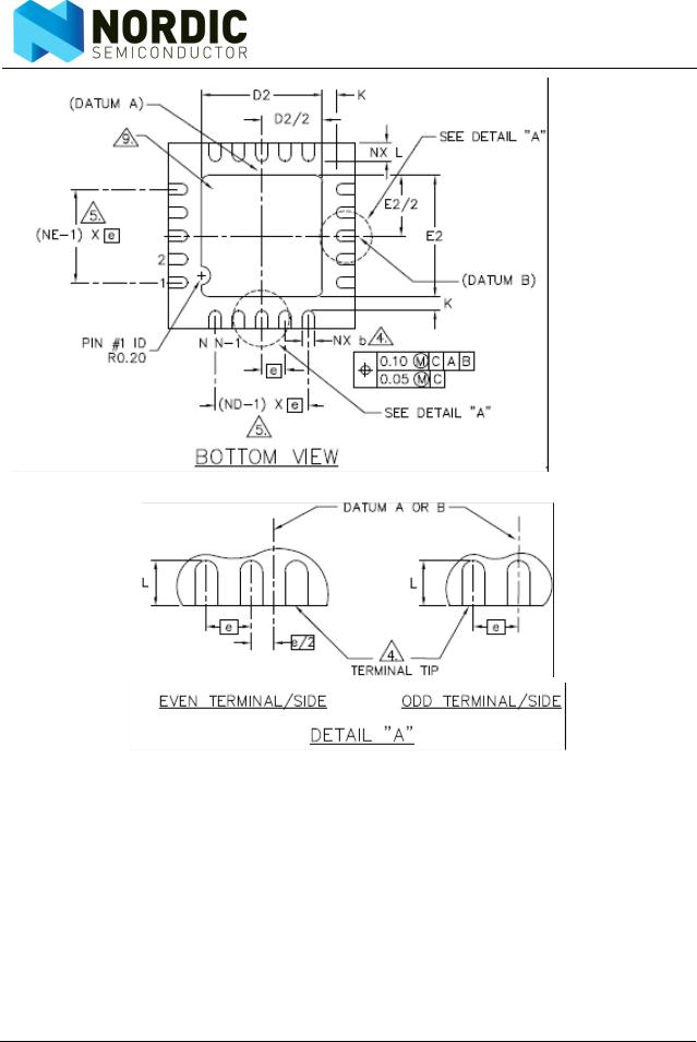
12 Mechanical specifications
nRF24L01+ uses the QFN20 4x4 package, with matt tin plating.
Revision 1.0 |
Page 71 of 78 |
nRF24L01+ Product Specification
Package Type |
|
A |
A1 |
A3 |
K |
D/E |
e |
D2/E2 |
L |
L1 |
b |
Saw QFN20 |
Min. |
0.80 |
0.00 |
|
|
|
|
2.50 |
0.35 |
|
0.18 |
(4x4 mm) |
Typ. |
0.85 |
0.02 |
0.20 |
0.20 |
4.0 |
0.5 BSC |
2.60 |
0.40 |
0.15 |
0.25 |
|
Max |
0.95 |
0.05 |
REF. |
min. |
BSCa |
|
2.70 |
0.45 |
max |
0.30 |
a. BSC: Basic Spacing between Centers, ref. JEDEC standard 95, page 4.17-11/A
Figure 39. nRF24L01+ Package Outline
Revision 1.0 |
Page 72 of 78 |