

nRF24L01+ Product Specification
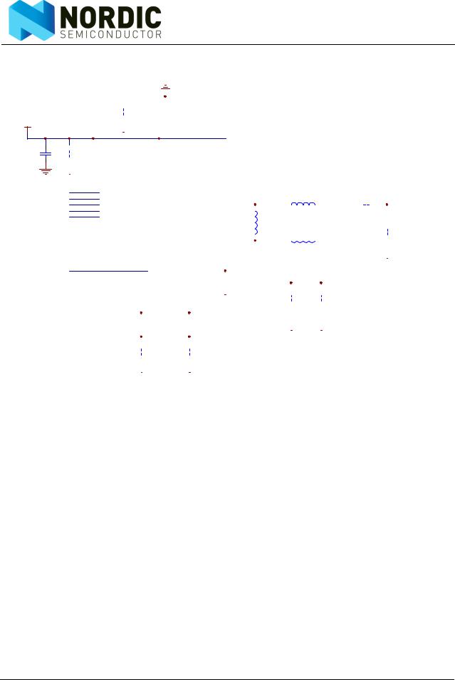
11 Application example
nRF24L01+ with single ended matching network crystal, bias resistor, and decoupling capacitors.
VDD
C9 |
|
|
|
|
|
C8 |
|
|
|||||||
|
|
|
|
||||
10nF |
|
|
|
|
1nF |
||
|
|||||||
0402 |
|
|
|
0402 |
|||
|
|
|
|
|
|
|
|
CE
CSN
SCK
MOSI
MISO
IRQ
|
|
|
|
|
|
|
|
|
|
|
|
|
|
|
|
|
|
|
|
|
|
|
|
|
|
|
|
|
|
|
|
|
|
|
|
|
|
|
|
|
|
|
|
|
|
|
|
|
|
|
|
|
|
|
|
|
|
|
|
|
|
|
|
|
|
|
|
|
|
|
|
|
|
|
|
|
|
|
|
|
|
|
|
|
|
|
|
|
|
|
|
|
|
|
|
|
|
|
|
|
|
|
|
|
|
|
|
|
|
|
|
|
|
|
|
|
|
|
|
|
|
|
|
|
|
|
|
|
|
|
|
|
|
|
|
|
|
|
|
|
|
|
C7 |
|
|
|
|
|
|
|
|
|
|
|
|
|
|
|
|
|
R2 |
|
|
|
|
|
|
|
|
|
|
|
|
|
|
|
|
|
|
|
|
|
|
|
|
|
|
|
|
|
|
|
|
|
|
|
||||||||||
|
|
|
|
|
33nF |
|
|
|
|
|
|
|
|
|
|
|
|
|
|
|
|
|
22K |
|
|
|
|
|
|
|
|
|
|
|
|
|
|
|
|
|
|
|
|
|
|
|
|
|
|
|
|
|
|
|
|
|
|
|
||||||||||
|
|
|
|
|
|
|
|
|
|
|
|
|
|
|
|
|
|
|
|
|
|
|
|
|
|
|
|
|
|
|
|
|
|
|
|
|
|
|
|
|
|
|
|
|
|
|
|
|
|
|
|
|
|
|
|
|
||||||||||||
|
|
|
|
|
|
|
|
|
|
|
|
|
|
|
|
|
|
|
|
|
|
|
|
|
|
|
|
|
|
|
|
|
|
|
|
|
|
|
|
|
|
|
|
|
|
|
|
|
|
|
|
|
|
|
||||||||||||||
|
|
|
0402 |
|
|
|
|
|
|
|
|
|
|
|
|
|
|
|
|
0402 |
|
|
|
|
|
|
|
|
|
|
|
|
|
|
|
|
|
|
|
|
|
|
|
|
|
|
|
|
|
|
|
|
|
|
|
|
|
|
|
|
||||||||
|
|
|
|
|
|
|
|
|
|
|
|
|
|
|
|
|
|
|
|
|
|
|
|
|
|
|
|
|
|
|
|
|
|
|
|
|
|
|
|
|
|
|
|
|
|
|
|
|
|
|
|
|
|
|
|
|
|
|
|
|
|
|
|
|
|
|
|
|
|
|
|
|
|
|
|
|
|
|
|
|
|
|
|
|
|
|
|
|
|
|
|
|
|
|
|
|
|
|
|
|
|
|
|
|
|
|
|
|
|
|
|
|
|
|
|
|
|
|
|
|
|
|
|
|
|
|
|
|
|
|
|||||||
|
|
|
|
|
|
|
|
20 |
|
19 |
|
18 |
|
17 |
|
16 |
|
|
|
|
|
|
|
|
|
|
|
|
|
|
|
|
|
|
|
|
|
|
|
|
|
|
|
|
|
|
|
|
|
|
|
|
|
|
|
|
|
|
|
|
|
|
||||||
|
|
|
|
|
|
|
|
|
|
|
|
|
|
|
|
|
|
|
|
|
|
|
|
|
|
|
|
|
|
|
|
|
|
|
|
|
|
|
|
|
|
|
|
|
|
|
|
|
|
|
|
|
|
|
|
|
|
|||||||||||
|
|
U1 |
|
|
|
|
|
|
|
|
|
|
|
|
|
|
|
|
|
|
|
|
|
|
|
|
|
|
|
|
|
|
|
|
|
|
|
|
|
|
|
|
|
|
|
|
|
|
|
|
|
|
|
|
|
|
|
|
|
|
|
|
|
|||||
|
|
|
|
|
|
|
|
VSS DVDD VDD VSS IREF |
|
|
|
|
|
|
|
|
|
|
|
|
|
|
|
|
|
|
|
|
|
|
|
|
|
|
|
|
|
|
|
|
|
|
|
|
|
|
|
|
|
|
|
|
|
|||||||||||||||
|
1 |
|
CE |
+ |
|
|
|
|
|
VDD |
|
15 |
|
|
|
|
|
|
|
|
|
|
|
|
|
|
|
|
|
|
C5 |
|||||||||||||||||||||||||||||||||||||
|
2 |
|
|
|
|
|
|
|
14 |
|
|
|
|
|
|
|
|
|
|
|
|
|
|
|
|
|
|
|||||||||||||||||||||||||||||||||||||||||
|
|
CSN |
|
|
|
nRF24L01 |
|
|
|
|
|
VSS |
|
|
|
|
|
|
|
|
|
|
|
L3 |
|
|
|
|
|
|
||||||||||||||||||||||||||||||||||||||
|
3 |
|
SCK |
|
|
|
|
|
|
|
|
|
|
|
|
|
|
|
|
|
|
|
|
ANT2 |
|
13 |
|
|
|
|
|
|
|
|
|
|
|
|
|
|
|
|
|
|
|
|
|
|
|
|
|
|
|
|
|
|
|
|
|
50ohm, |
||||||||
|
4 |
|
MOSI |
|
|
|
|
|
|
|
|
|
|
|
|
|
|
|
|
|
|
|
|
ANT1 |
|
12 |
|
|
|
|
|
|
|
|
|
L1 |
3.9nH |
|
|
|
|
|
|
|
|
|
|
|
|
|
|
|
|
|
|
|
|
|
|
|||||||||
|
5 |
|
MISO |
|
|
|
|
|
|
|
|
|
|
|
|
|
|
|
|
|
VDD_PA |
|
11 |
|
|
|
|
|
|
|
|
|
0402 |
|
|
|
|
|
|
1.5pF |
|
|
|
|||||||||||||||||||||||||
|
|
|
|
|
|
|
|
|
|
|
|
|
|
|
|
|
|
|
|
|
|
|
|
|
|
|
|
|
|
|
|
|
|
|
|
|
|
|
|
|
|
|
|
8.2nH |
|
|
0402 |
|
|
|
|
|
|
|
|
|
|
|
||||||||||
|
|
|
|
|
|
|
|
IRQ VDD VSS XC2 XC1 |
|
|
|
|
|
|
|
|
|
|
|
|
|
|
0402 |
|
|
|
|
|
|
|
|
|
|
|
|
|
|
|
|
|
|
|
|
|
|
C6 |
||||||||||||||||||||||
|
|
|
|
|
|
|
|
|
|
|
|
|
|
|
|
|
|
|
|
|
|
|
|
|
|
|
|
|
|
|
|
|
|
|
|
|
|
|
|
|
|
|
|
|
|
|
|
|
|
|
||||||||||||||||||
|
|
|
|
|
|
|
|
|
|
|
|
|
|
|
|
|
|
|
|
|
|
|
|
|
|
|
|
|
|
|
|
|
|
|
|
|
|
|
|
|
|
|
|
|
|
|
|
|
|
|||||||||||||||||||
|
|
|
|
|
|
|
|
|
|
|
|
|
|
|
|
|
|
|
|
|
|
|
|
|
|
|
|
|
|
|
|
|
|
|
|
|
|
|
|
|
|
|
|
|
L2 |
|
|
|
|
|
|
|
|
|
|
|
|
|
|
|
|
|
1.0pF |
|||||
|
|
|
|
|
|
|
|
|
|
|
|
|
|
|
|
|
|
|
|
|
|
|
|
|
|
|
|
|
|
|
|
|
|
|
|
|
|
|
|
|
|
|
|
|
|
|
|
|
|
|||||||||||||||||||
|
|
|
|
|
|
|
|
|
|
|
|
|
|
|
|
|
|
|
|
|
|
|
|
|
|
|
|
|
|
|
|
|
|
|
|
|
|
|
|
|
|
|
|
|
2.7nH |
|
|
|
|
|
|
|
0402 |
|
||||||||||||||
|
|
|
|
|
|
|
|
|
|
|
|
|
|
|
|
|
|
|
|
|
|
|
|
|
NRF24L01 |
|
|
|
|
|
|
|
|
|
|
|
0402 |
|
|
|
|
|
|
|
|
|
|
|
|
|
|
|
|
|
|
|
|
|
|
|||||||||
|
|
|
|
|
|
|
|
6 |
|
7 |
|
8 |
|
9 |
|
10 |
|
|
|
|
|
|
|
|
|
|
|
|
|
|
|
|
|
|
|
|
|
|
|
|
|
|
|
|
|
|
|
|
|
|
|
|
|
|
|
|
|
|
|
|
|
|
||||||
|
|
|
|
|
|
|
|
|
|
|
|
|
|
|
|
|
|
|
|
|
|
|
|
|
|
|
|
|
|
|
|
|
|
|
|
|
|
|
|
|
|
|
|
|
|
|
|
|
|
|
|
|
|
|
|
|
|
|
|
|
|
|
|
|
|
|
|
|
|
|
|
|
|
|
|
|
|
|
|
|
|
|
|
|
|
|
|
|
|
|
|
|
|
|
|
|
|
|
|
|
|
|
|
|
|
|
|
|
|
|
|
|
|
|
|
|
|
|
|
|
|
|
|
|
|
|
|
|
|
|
|
|
|
|
|
|
|
|
|
|
|
|
|
|
|
|
|
|
|
|
|
|
|
|
|
|
|
|
|
|
|
|
|
|
|
|
|
|
|
|
|
|
|
|
|
|
|
|
|
|
|
|
|
|
|
|
|
|
|
|
|
|
|
|
|
|
|
|
|
|
|
|
|
|
|
|
|
|
|
|
|
|
|
|
|
|
|
|
|
|
|
|
|
|
|
|
|
|
|
|
|
|
|
|
|
|
|
|
|
|
|
|
|
|
|
|
|
|
|
|
|
|
|
|
|
|
|
|
|
|
|
|
|
|
|
|
|
|
|
|
|
|
|
|
|
|
|
|
|
|
|
|
|
|
|
|
|
|
|
|
|
|
|
|
|
|
|
|
|
|
|
|
|
|
|
|
|
|
|
|
|
|
|
|
|
|
|
|
|
|
|
C3 |
|
|
|
|
C4 |
|||||||||||||||||
|
|
|
|
|
|
|
|
|
|
|
|
|
|
|
|
|
|
|
|
X1 |
|
|
|
|
|
|
|
|
|
|
|
|
|
|
|
|
|
|
|
|
|
|
|
|
|
|
||||||||||||||||||||||
|
|
|
|
|
|
|
|
|
|
|
|
|
|
|
|
|
|
|
|
|
|
|
|
|
|
|
|
|
|
|
|
|
|
|
|
|
|
|
|
|
|
|
|
|
|
2.2nF |
|
|
|
|
4.7pF |
|||||||||||||||||
|
|
|
|
|
|
|
|
|
|
|
|
|
|
|
|
|
|
|
|
|
|
|
|
|
|
|
|
|
|
|
|
|
|
|
|
|
|
|
|
|
|
|
|
|
||||||||||||||||||||||||
|
|
|
|
|
|
|
|
|
|
|
|
|
|
|
|
|
|
|
|
|
|
|
|
|
|
|
|
|
|
|
|
|
|
|
|
|
|
|
|
|
|
|
|
|
0402 |
|
0402 |
|
|
|
|
|
|
|
|
|
|
|
|
|
|
|
|
|||||
|
|
|
|
|
|
|
|
|
|
|
|
|
|
|
|
|
|
|
|
|
|
|
|
|
|
|
|
|
|
|
|
|
|
|
|
|
|
|
|
|
|
|
|
|
|
|
|
|
|
|
|
|
|
|
|
|
|
|
|
|
|
|
|
|
|
|
||
|
|
|
|
|
|
|
|
|
|
|
|
|
|
|
|
|
|
|
|
|
|
|
|
|
|
|
|
|
|
|
|
|
|
|
|
|
|
|
|
|
|
|
|
|
|
|
|
|
|
|
|
|
|
|
|
|
|
|
|
|
|
|
|
|
|
|
|
|
|
|
|
|
|
|
|
|
|
|
|
|
|
16 MHz |
|
|
|
|
|
|
|
|
|
|
|
|
|
|
|
|
|
|
|
|
|
|
|
|
|
|
|
|
|
|
|
|
|
|
|
|
|
|
|
|
|
|
|
|
|
||||||||||
|
|
|
|
|
|
|
|
|
|
|
|
|
|
|
|
R1 |
|
|
|
|
|
|
|
|
|
|
|
|
|
|
|
|
|
|
|
|
|
|
|
|
|
|
|
|
|
|
|
|
|
|
|
|
|
|
|
|
|
|
|
|
|
|||||||
|
|
|
|
|
|
|
|
|
|
|
|
|
|
|
|
|
1M |
|
|
|
|
|
|
|
|
|
|
|
|
|
|
|
|
|
|
|
|
|
|
|
|
|
|
|
|
|
|
|
|
|
|
|
|
|
|
|
|
|
|
|
|
|
||||||
|
|
|
|
|
|
|
|
|
|
|
|
|
|
|
|
|
|
|
|
|
|
|
|
|
|
|
|
|
|
|
|
|
|
|
|
|
|
|
|
|
|
|
|
|
|
|
|
|
|
|
|
|
||||||||||||||||
|
|
|
|
|
|
|
|
|
|
|
|
|
C1 |
|
|
|
|
|
|
|
|
C2 |
|
|
|
|
|
|
|
|
|
|
|
|
|
|
|
|
|
|
|
|
|
|
|
|
|
|
|
|
|
|
|
|
|
|
|
|||||||||||
|
|
|
|
|
|
|
|
|
|
|
|
|
|
|
|
|
|
|
|
|
|
|
|
|
|
|
|
|
|
|
|
|
|
|
|
|
|
|
|
|
|
|
|
|
|
|
|
|||||||||||||||||||||
|
|
|
|
|
|
|
|
|
|
|
|
|
|
|
|
|
|
|
|
|
|
|
|
|
|
|
|
|
|
|
|
|
|
|
|
|
|
|
|
|
|
|
|
|
|
|
|
|
|
|
|
|||||||||||||||||
|
|
|
|
|
|
|
|
|
|
|
|
|
22pF |
|
|
|
|
|
|
|
|
22pF |
|
|
|
|
|
|
|
|
|
|
|
|
|
|
|
|
|
|
|
|
|
|
|
|
|
|
|
|
|
|
|
|
|
|
|
|||||||||||
|
|
|
|
|
|
|
|
|
|
|
|
|
|
|
|
|
|
|
|
|
|
|
|
|
|
|
|
|
|
|
|
|
|
|
|
|
|
|
|
|
|
|
|
|
|
|
|
|||||||||||||||||||||
|
|
|
|
|
|
|
|
0402 |
|
|
|
|
|
|
|
|
|
0402 |
|
|
|
|
|
|
|
|
|
|
|
|
|
|
|
|
|
|
|
|
|
|
|
|
|
|
|
|
|
|
|
|
|
|
|
|||||||||||||||
|
|
|
|
|
|
|
|
|
|
|
|
|
|
|
|
|
|
|
|
|
|
|
|
|
|
|
|
|
|
|
|
|
|
|
|
|
|
|
|
|
|
|
|
|
|
|
|
|
|
|
|
|
|
|
|
|
|
|
|
|
|
|
|
|
|
|
|
|
Figure 32. nRF24L01+ schematic for RF layouts with single ended 50Ω RF output
Revision 1.0 |
Page 66 of 78 |

nRF24L01+ Product Specification
Part |
Designator |
Footprint |
Description |
22pFa |
C1 |
0402 |
NPO, +/- 2% |
22pFa |
C2 |
0402 |
NPO, +/- 2% |
2.2nF |
C3 |
0402 |
X7R, +/- 10% |
4.7pF |
C4 |
0402 |
NPO, +/- 0.25pF |
1.5pF |
C5 |
0402 |
NPO, +/- 0.1pF |
1,0pF |
C6 |
0402 |
NPO, +/- 0.1pF |
33nF |
C7 |
0402 |
X7R, +/- 10% |
1nF |
C8 |
0402 |
X7R, +/- 10% |
10nF |
C9 |
0402 |
X7R, +/- 10% |
8,2nH |
L1 |
0402 |
chip inductor +/- 5% |
2.7nH |
L2 |
0402 |
chip inductor +/- 5% |
3,9nH |
L3 |
0402 |
chip inductor +/- 5% |
Not mountedb |
R1 |
0402 |
|
22kΩ |
R2 |
0402 |
+/-1% |
nRF24L01+ |
U1 |
QFN20 4x4 |
|
16MHz |
X1 |
|
+/-60ppm, CL=12pF |
a.C1 and C2 must have values that match the crystals load capacitance, CL.
b.The nRF24L01+ and nRF24L01 application example and BOM are the same with the exception of R1. R1 can be mounted for backward compatibility with nRF24L01. The use of a 1Mohm resistor externally does not have any impact on crystal performance.
Table 29. Recommended components (BOM) in nRF24L01+ with antenna matching network
11.1PCB layout examples
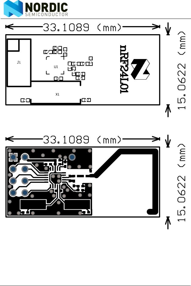
Figure 33., Figure 34. and Figure 35. show a PCB layout example for the application schematic in Figure 32..
A double-sided FR-4 board of 1.6mm thickness is used. This PCB has a ground plane on the bottom layer. Additionally, there are ground areas on the component side of the board to ensure sufficient grounding of critical components. A large number of via holes connect the top layer ground areas to the bottom layer ground plane.
Revision 1.0 |
Page 67 of 78 |
nRF24L01+ Product Specification
+
Figure 33. Top overlay (nRF24L01+ RF layout with single ended connection to PCB antenna and 0402 size passive components)
Figure 34. Top layer (nRF24L01+ RF layout with single ended connection to PCB antenna and 0402 size passive components)
Revision 1.0 |
Page 68 of 78 |
nRF24L01+ Product Specification
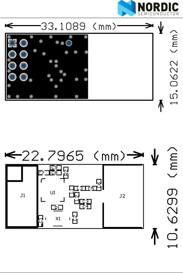
Figure 35. Bottom layer (nRF24L01+ RF layout with single ended connection to PCB antenna and 0402 size passive components
The nest figure (Figure 36., Figure 37. and Figure 38.) is for the SMA output to have a board for direct measurements at a 50Ω SMA connector.
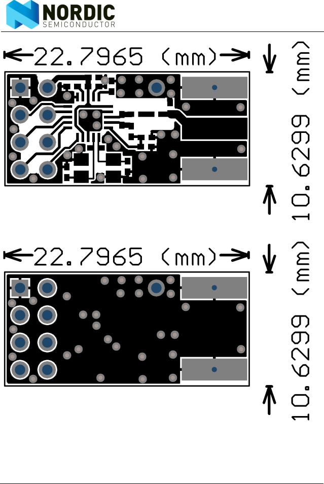
Figure 36. Top Overlay (Module with OFM crystal and SMA connector)
Revision 1.0 |
Page 69 of 78 |
nRF24L01+ Product Specification
Figure 37. Top Layer (Module with OFM crystal and SMA connector)
Figure 38. Bottom Layer (Module with OFM crystal and SMA connector)
Revision 1.0 |
Page 70 of 78 |