- •CONTENTS
- •1.2 Overview of Volume 1: Basic Architecture
- •1.3 Notational Conventions
- •1.3.1 Bit and Byte Order
- •1.3.2 Reserved Bits and Software Compatibility
- •1.3.3 Instruction Operands
- •1.3.4 Hexadecimal and Binary Numbers
- •1.3.5 Segmented Addressing
- •1.3.6 A New Syntax for CPUID, CR, and MSR Values
- •1.3.7 Exceptions
- •1.4 Related Literature
- •2.1.10 The Intel Pentium Processor Extreme Edition (2005)
- •2.2 More on SPECIFIC advances
- •2.2.1 P6 Family Microarchitecture
- •2.2.2.1 The Front End Pipeline
- •2.2.2.3 Retirement Unit
- •2.2.3 SIMD Instructions
- •2.2.4 Hyper-Threading Technology
- •2.2.4.1 Some Implementation Notes
- •3.1 Modes of Operation
- •3.2 Overview of the Basic Execution Environment
- •3.3 Memory Organization
- •3.3.1 Three Memory Models
- •3.3.2 Paging and Virtual Memory
- •3.3.4 Modes of Operation vs. Memory Model
- •3.3.6 Extended Physical Addressing in Protected Mode
- •3.3.7.1 Canonical Addressing
- •3.4 Basic Program Execution Registers
- •3.4.2 Segment Registers
- •3.4.3 EFLAGS Register
- •3.4.3.1 Status Flags
- •3.4.3.2 DF Flag
- •3.4.3.3 System Flags and IOPL Field
- •3.5 Instruction Pointer
- •3.7 Operand Addressing
- •3.7.1 Immediate Operands
- •3.7.2 Register Operands
- •3.7.3 Memory Operands
- •3.7.4 Specifying a Segment Selector
- •3.7.5 Specifying an Offset
- •3.7.6 Assembler and Compiler Addressing Modes
- •3.7.7 I/O Port Addressing
- •4.1 Fundamental Data Types
- •4.1.1 Alignment of Words, Doublewords, Quadwords, and Double Quadwords
- •4.2 Numeric Data Types
- •4.2.1 Integers
- •4.2.1.1 Unsigned Integers
- •4.2.1.2 Signed Integers
- •4.3 Pointer Data Types
- •4.4 Bit Field Data Type
- •4.5 String Data Types
- •4.6 Packed SIMD Data Types
- •4.6.2 128-Bit Packed SIMD Data Types
- •4.7 BCD and Packed BCD Integers
- •4.8.1 Real Number System
- •4.8.2.1 Normalized Numbers
- •4.8.2.2 Biased Exponent
- •4.8.3.1 Signed Zeros
- •4.8.3.2 Normalized and Denormalized Finite Numbers
- •4.8.3.3 Signed Infinities
- •4.8.3.4 NaNs
- •4.8.3.5 Operating on SNaNs and QNaNs
- •4.8.3.6 Using SNaNs and QNaNs in Applications
- •4.8.4 Rounding
- •4.8.4.1 Rounding Control (RC) Fields
- •4.8.4.2 Truncation with SSE and SSE2 Conversion Instructions
- •4.9.1.1 Invalid Operation Exception (#I)
- •4.9.1.2 Denormal Operand Exception (#D)
- •4.9.1.4 Numeric Overflow Exception (#O)
- •4.9.1.5 Numeric Underflow Exception (#U)
- •5.1.1 Data Transfer Instructions
- •5.1.2 Binary Arithmetic Instructions
- •5.1.3 Decimal Arithmetic Instructions
- •5.1.4 Logical Instructions
- •5.1.5 Shift and Rotate Instructions
- •5.1.6 Bit and Byte Instructions
- •5.1.7 Control Transfer Instructions
- •5.1.8 String Instructions
- •5.1.9 I/O Instructions
- •5.1.10 Enter and Leave Instructions
- •5.1.11 Flag Control (EFLAG) Instructions
- •5.1.12 Segment Register Instructions
- •5.1.13 Miscellaneous Instructions
- •5.2 x87 FPU Instructions
- •5.2.1 x87 FPU Data Transfer Instructions
- •5.2.2 x87 FPU Basic Arithmetic Instructions
- •5.2.3 x87 FPU Comparison Instructions
- •5.2.4 x87 FPU Transcendental Instructions
- •5.2.5 x87 FPU Load Constants Instructions
- •5.2.6 x87 FPU Control Instructions
- •5.3 x87 FPU AND SIMD State Management Instructions
- •5.4.1 MMX Data Transfer Instructions
- •5.4.2 MMX Conversion Instructions
- •5.4.3 MMX Packed Arithmetic Instructions
- •5.4.4 MMX Comparison Instructions
- •5.4.5 MMX Logical Instructions
- •5.4.6 MMX Shift and Rotate Instructions
- •5.4.7 MMX State Management Instructions
- •5.5 SSE Instructions
- •5.5.1.1 SSE Data Transfer Instructions
- •5.5.1.2 SSE Packed Arithmetic Instructions
- •5.5.1.3 SSE Comparison Instructions
- •5.5.1.4 SSE Logical Instructions
- •5.5.1.5 SSE Shuffle and Unpack Instructions
- •5.5.1.6 SSE Conversion Instructions
- •5.5.2 SSE MXCSR State Management Instructions
- •5.5.4 SSE Cacheability Control, Prefetch, and Instruction Ordering Instructions
- •5.6 SSE2 Instructions
- •5.6.1.1 SSE2 Data Movement Instructions
- •5.6.1.2 SSE2 Packed Arithmetic Instructions
- •5.6.1.3 SSE2 Logical Instructions
- •5.6.1.4 SSE2 Compare Instructions
- •5.6.1.5 SSE2 Shuffle and Unpack Instructions
- •5.6.1.6 SSE2 Conversion Instructions
- •5.6.4 SSE2 Cacheability Control and Ordering Instructions
- •5.7 SSE3 Instructions
- •5.7.6 SSE3 Agent Synchronization Instructions
- •5.8 System Instructions
- •CHAPTER 6 Procedure Calls, Interrupts, and Exceptions
- •6.1 Procedure Call Types
- •6.2 Stacks
- •6.2.1 Setting Up a Stack
- •6.2.2 Stack Alignment
- •6.2.4 Procedure Linking Information
- •6.2.4.2 Return Instruction Pointer
- •6.3 Calling Procedures Using CALL and RET
- •6.3.1 Near CALL and RET Operation
- •6.3.2 Far CALL and RET Operation
- •6.3.3 Parameter Passing
- •6.3.3.2 Passing Parameters on the Stack
- •6.3.3.3 Passing Parameters in an Argument List
- •6.3.4 Saving Procedure State Information
- •6.3.5 Calls to Other Privilege Levels
- •6.3.6 CALL and RET Operation Between Privilege Levels
- •6.4 Interrupts and Exceptions
- •6.4.1 Call and Return Operation for Interrupt or Exception Handling Procedures
- •6.4.2 Calls to Interrupt or Exception Handler Tasks
- •6.5.1 ENTER Instruction
- •6.5.2 LEAVE Instruction
- •CHAPTER 7 Programming With General-Purpose Instructions
- •7.1 Programming environment for gp Instructions
- •7.3 Summary of gp Instructions
- •7.3.1. Data Transfer Instructions
- •7.3.1.1 General Data Movement Instructions
- •7.3.1.2 Exchange Instructions
- •7.3.1.4 Stack Manipulation Instructions
- •7.3.1.6 Type Conversion Instructions
- •7.3.2. Binary Arithmetic Instructions
- •7.3.2.1 Addition and Subtraction Instructions
- •7.3.2.2 Increment and Decrement Instructions
- •7.3.2.4 Comparison and Sign Change Instruction
- •7.3.2.5 Multiplication and Divide Instructions
- •7.3.3. Decimal Arithmetic Instructions
- •7.3.3.1 Packed BCD Adjustment Instructions
- •7.3.3.2 Unpacked BCD Adjustment Instructions
- •7.3.5. Logical Instructions
- •7.3.6. Shift and Rotate Instructions
- •7.3.6.1 Shift Instructions
- •7.3.6.3 Rotate Instructions
- •7.3.7. Bit and Byte Instructions
- •7.3.7.1 Bit Test and Modify Instructions
- •7.3.7.2 Bit Scan Instructions
- •7.3.7.3 Byte Set on Condition Instructions
- •7.3.7.4 Test Instruction
- •7.3.8. Control Transfer Instructions
- •7.3.8.1 Unconditional Transfer Instructions
- •7.3.8.2 Conditional Transfer Instructions
- •7.3.8.4 Software Interrupt Instructions
- •7.3.9. String Operations
- •7.3.9.1 Repeating String Operations
- •7.3.10. String Operations in 64-Bit Mode
- •7.3.11. I/O Instructions
- •7.3.12. I/O Instructions in 64-Bit Mode
- •7.3.13. Enter and Leave Instructions
- •7.3.14. Flag Control (EFLAG) Instructions
- •7.3.14.1 Carry and Direction Flag Instructions
- •7.3.14.2 EFLAGS Transfer Instructions
- •7.3.14.3 Interrupt Flag Instructions
- •7.3.15. Flag Control (RFLAG) Instructions in 64-Bit Mode
- •7.3.16. Segment Register Instructions
- •7.3.16.2 Far Control Transfer Instructions
- •7.3.16.3 Software Interrupt Instructions
- •7.3.16.4 Load Far Pointer Instructions
- •7.3.17. Miscellaneous Instructions
- •7.3.17.1 Address Computation Instruction
- •7.3.17.2 Table Lookup Instructions
- •7.3.17.3 Processor Identification Instruction
- •8.1 x87 FPU Execution Environment
- •8.1.2 x87 FPU Data Registers
- •8.1.2.1 Parameter Passing With the x87 FPU Register Stack
- •8.1.3 x87 FPU Status Register
- •8.1.3.1 Top of Stack (TOP) Pointer
- •8.1.3.2 Condition Code Flags
- •8.1.3.4 Stack Fault Flag
- •8.1.4 Branching and Conditional Moves on Condition Codes
- •8.1.5 x87 FPU Control Word
- •8.1.5.2 Precision Control Field
- •8.1.5.3 Rounding Control Field
- •8.1.6 Infinity Control Flag
- •8.1.7 x87 FPU Tag Word
- •8.1.8 x87 FPU Instruction and Data (Operand) Pointers
- •8.1.9 Last Instruction Opcode
- •8.1.10 Saving the x87 FPU’s State with FSTENV/FNSTENV and FSAVE/FNSAVE
- •8.1.11 Saving the x87 FPU’s State with FXSAVE
- •8.2 x87 FPU Data Types
- •8.2.1 Indefinites
- •8.3 x86 FPU Instruction Set
- •8.3.1 Escape (ESC) Instructions
- •8.3.2 x87 FPU Instruction Operands
- •8.3.3 Data Transfer Instructions
- •8.3.4 Load Constant Instructions
- •8.3.5 Basic Arithmetic Instructions
- •8.3.6 Comparison and Classification Instructions
- •8.3.6.1 Branching on the x87 FPU Condition Codes
- •8.3.7 Trigonometric Instructions
- •8.3.9 Logarithmic, Exponential, and Scale
- •8.3.10 Transcendental Instruction Accuracy
- •8.3.11 x87 FPU Control Instructions
- •8.3.13 Unsupported x87 FPU Instructions
- •8.5.1 Invalid Operation Exception
- •8.5.1.1 Stack Overflow or Underflow Exception (#IS)
- •8.5.1.2 Invalid Arithmetic Operand Exception (#IA)
- •8.5.2 Denormal Operand Exception (#D)
- •8.5.4 Numeric Overflow Exception (#O)
- •8.5.5 Numeric Underflow Exception (#U)
- •8.6 x87 FPU Exception Synchronization
- •8.7 Handling x87 FPU Exceptions in Software
- •8.7.1 Native Mode
- •8.7.3 Handling x87 FPU Exceptions in Software
- •9.1 Overview of MMX Technology
- •9.2 The MMX Technology Programming Environment
- •9.2.2 MMX Registers
- •9.2.3 MMX Data Types
- •9.2.4 Memory Data Formats
- •9.2.5 Single Instruction, Multiple Data (SIMD) Execution Model
- •9.3 Saturation and Wraparound Modes
- •9.4 MMX Instructions
- •9.4.1 Data Transfer Instructions
- •9.4.2 Arithmetic Instructions
- •9.4.3 Comparison Instructions
- •9.4.4 Conversion Instructions
- •9.4.5 Unpack Instructions
- •9.4.6 Logical Instructions
- •9.4.7 Shift Instructions
- •9.4.8 EMMS Instruction
- •9.5 Compatibility with x87 FPU Architecture
- •9.5.1 MMX Instructions and the x87 FPU Tag Word
- •9.6 WRITING APPLICATIONS WITH MMX CODE
- •9.6.1 Checking for MMX Technology Support
- •9.6.2 Transitions Between x87 FPU and MMX Code
- •9.6.3 Using the EMMS Instruction
- •9.6.4 Mixing MMX and x87 FPU Instructions
- •9.6.5 Interfacing with MMX Code
- •9.6.6 Using MMX Code in a Multitasking Operating System Environment
- •9.6.7 Exception Handling in MMX Code
- •9.6.8 Register Mapping
- •9.6.9 Effect of Instruction Prefixes on MMX Instructions
- •CHAPTER 10 Programming with Streaming SIMD Extensions (SSE)
- •10.1 Overview of SSE Extensions
- •10.2 SSE Programming Environment
- •10.2.2 XMM Registers
- •10.2.3 MXCSR Control and Status Register
- •10.2.3.3 Flush-To-Zero
- •10.2.3.4 Denormals-Are-Zeros
- •10.2.4 Compatibility of SSE Extensions with SSE2/SSE3/MMX and the x87 FPU
- •10.3 SSE Data Types
- •10.4 SSE Instruction Set
- •10.4.1.1 SSE Data Movement Instructions
- •10.4.1.2 SSE Arithmetic Instructions
- •10.4.2 SSE Logical Instructions
- •10.4.2.1 SSE Comparison Instructions
- •10.4.2.2 SSE Shuffle and Unpack Instructions
- •10.4.3 SSE Conversion Instructions
- •10.4.5 MXCSR State Management Instructions
- •10.4.6 Cacheability Control, Prefetch, and Memory Ordering Instructions
- •10.4.6.1 Cacheability Control Instructions
- •10.4.6.4 SFENCE Instruction
- •10.5 FXSAVE and FXRSTOR Instructions
- •10.6 Handling SSE Instruction Exceptions
- •10.7 Writing Applications with the SSE Extensions
- •CHAPTER 11 Programming with Streaming SIMD Extensions 2 (SSE2)
- •11.1 Overview of SSE2 Extensions
- •11.2 SSE2 Programming Environment
- •11.2.2 Compatibility of SSE2 Extensions with SSE, MMX Technology and x87 FPU Programming Environment
- •11.3 SSE2 Data Types
- •11.4 SSE2 Instructions
- •11.4.1.1 Data Movement Instructions
- •11.4.1.2 SSE2 Arithmetic Instructions
- •11.4.1.3 SSE2 Logical Instructions
- •11.4.1.4 SSE2 Comparison Instructions
- •11.4.1.5 SSE2 Shuffle and Unpack Instructions
- •11.4.1.6 SSE2 Conversion Instructions
- •11.4.4 Cacheability Control and Memory Ordering Instructions
- •11.4.4.1 FLUSH Cache Line
- •11.4.4.2 Cacheability Control Instructions
- •11.4.4.3 Memory Ordering Instructions
- •11.4.4.4 Pause
- •11.4.5 Branch Hints
- •11.5 SSE, SSE2, and SSE3 Exceptions
- •11.5.1 SIMD Floating-Point Exceptions
- •11.5.2.1 Invalid Operation Exception (#I)
- •11.5.2.4 Numeric Overflow Exception (#O)
- •11.5.2.5 Numeric Underflow Exception (#U)
- •11.5.3.1 Handling Masked Exceptions
- •11.5.3.2 Handling Unmasked Exceptions
- •11.5.3.3 Handling Combinations of Masked and Unmasked Exceptions
- •11.6 Writing Applications with SSE/SSE2 Extensions
- •11.6.1 General Guidelines for Using SSE/SSE2 Extensions
- •11.6.2 Checking for SSE/SSE2 Support
- •11.6.3 Checking for the DAZ Flag in the MXCSR Register
- •11.6.4 Initialization of SSE/SE2 Extensions
- •11.6.5 Saving and Restoring the SSE/SSE2 State
- •11.6.6 Guidelines for Writing to the MXCSR Register
- •11.6.7 Interaction of SSE/SSE2 Instructions with x87 FPU and MMX Instructions
- •11.6.10 Interfacing with SSE/SSE2 Procedures and Functions
- •11.6.10.1 Passing Parameters in XMM Registers
- •11.6.10.2 Saving XMM Register State on a Procedure or Function Call
- •11.6.12 Branching on Arithmetic Operations
- •11.6.13 Cacheability Hint Instructions
- •11.6.14 Effect of Instruction Prefixes on the SSE/SSE2 Instructions
- •CHAPTER 12 Programming with Streaming SIMD Extensions 3 (SSE3)
- •12.1 Overview of SSE3 Instructions
- •12.2 SSE3 Programming Environment and Data types
- •12.2.2 Compatibility of SSE3 Extensions with MMX Technology, the x87 FPU Environment, and SSE/SSE2 Extensions
- •12.2.3 Horizontal and Asymmetric Processing
- •12.3 SSE3 Instructions
- •12.3.1 x87 FPU Instruction for Integer Conversion
- •12.3.6 Two Thread Synchronization Instructions
- •12.4 SSE3 Exceptions
- •12.4.1 Device Not Available (DNA) Exceptions
- •12.4.2 Numeric Error flag and IGNNE#
- •12.4.3 Emulation
- •12.5 Writing Applications with SSE3 Extensions
- •12.5.1 General Guidelines for Using SSE3 Extensions
- •12.5.2 Checking for SSE3 Support
- •12.5.4 Programming SSE3 with SSE/SSE2 Extensions
- •13.1 I/O Port Addressing
- •13.2 I/O Port Hardware
- •13.3 I/O Address Space
- •13.4 I/O Instructions
- •13.5.1 I/O Privilege Level
- •13.5.2 I/O Permission Bit Map
- •13.6 Ordering I/O
- •CHAPTER 14 Processor Identification and Feature Determination
- •14.1 Using the CPUID Instruction
- •14.1.1 Notes on Where to Start
- •A.1 EFLAGS and Instructions
- •B.1 Condition Codes
- •APPENDIX C Floating-Point Exceptions Summary
- •C.1 Overview
- •C.2 x87 FPU Instructions
- •C.3 SSE Instructions
- •C.4 SSE2 Instructions
- •C.5 SSE3 Instructions
- •D.1 Origin of the MS-DOS Compatibility Sub-mode for Handling x87 FPU Exceptions
- •D.2 Implementation of the MS-DOS Compatibility Sub-mode In the Intel486, Pentium, AND P6 Processor Family, and Pentium 4 Processors
- •D.2.1.1 Basic Rules: When FERR# Is Generated
- •D.2.1.2 Recommended External Hardware to Support the MS-DOS Compatibility Sub-mode
- •D.2.1.3 No-Wait x87 FPU Instructions Can Get x87 FPU Interrupt in Window
- •D.2.2 MS-DOS Compatibility Sub-mode in the P6 Family and Pentium 4 Processors
- •D.3 Recommended Protocol for MS-DOS* Compatibility Handlers
- •D.3.1 Floating-Point Exceptions and Their Defaults
- •D.3.2 Two Options for Handling Numeric Exceptions
- •D.3.2.1 Automatic Exception Handling: Using Masked Exceptions
- •D.3.2.2 Software Exception Handling
- •D.3.3 Synchronization Required for Use of x87 FPU Exception Handlers
- •D.3.3.1 Exception Synchronization: What, Why and When
- •D.3.3.2 Exception Synchronization Examples
- •D.3.3.3 Proper Exception Synchronization
- •D.3.4 x87 FPU Exception Handling Examples
- •D.3.6 Considerations When x87 FPU Shared Between Tasks
- •D.3.6.1 Speculatively Deferring x87 FPU Saves, General Overview
- •D.3.6.2 Tracking x87 FPU Ownership
- •D.3.6.4 Interrupt Routing From the Kernel
- •D.3.6.5 Special Considerations for Operating Systems that Support Streaming SIMD Extensions
- •D.4 Differences For Handlers Using Native Mode
- •D.4.1 Origin with the Intel 286 and Intel 287, and Intel386 and Intel 387 Processors
- •D.4.2 Changes with Intel486, Pentium and Pentium Pro Processors with CR0.NE[bit 5] = 1
- •D.4.3 Considerations When x87 FPU Shared Between Tasks Using Native Mode
- •APPENDIX E Guidelines for Writing SIMD Floating-Point Exception Handlers
- •E.1 Two Options for Handling Floating-Point Exceptions
- •E.2 Software Exception Handling
- •E.3 Exception Synchronization
- •E.4 SIMD Floating-Point Exceptions and the IEEE Standard 754
- •E.4.1 Floating-Point Emulation
- •E.4.2 SSE/SSE2/SSE3 Response To Floating-Point Exceptions
- •E.4.2.1 Numeric Exceptions
- •E.4.2.2 Results of Operations with NaN Operands or a NaN Result for SSE/SSE2/SSE3 Numeric Instructions
- •E.4.2.3 Condition Codes, Exception Flags, and Response for Masked and Unmasked Numeric Exceptions
- •E.4.3 Example SIMD Floating-Point Emulation Implementation
- •INDEX
- •INTEL SALES OFFICES
PROGRAMMING WITH INTEL MMX TECHNOLOGY
•Chapter 11, MMX Technology System Programming Model, in the IA-32 Intel Architecture Software Developer’s Manual, Volume 3 describes the manner in which MMX technology is integrated into the IA-32 system programming model.
9.2THE MMX TECHNOLOGY PROGRAMMING ENVIRONMENT
Figure 9-1 shows the execution environment for MMX technology. All MMX instructions operate on MMX registers, the general-purpose registers, and/or memory as follows:
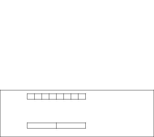
•MMX registers — These eight registers (see Figure 9-1) are used to perform operations on 64-bit packed integer data. They are named MM0 through MM7.
Address Space
232 -1
MMX Registers
Eight 64-Bit
General-Purpose
Registers
Eight 32-Bit
0
Figure 9-1. MMX Technology Execution Environment
•General-purpose registers — The eight general-purpose registers (see Figure 3-5) are used with existing IA-32 addressing modes to address operands in memory. (MMX registers cannot be used to address memory). General-purpose registers are also used to hold operands for some MMX technology operations. They are EAX, EBX, ECX, EDX, EBP, ESI, EDI, and ESP.
9.2.1MMX Technology in 64-Bit Mode and Compatibility Mode
In compatibility mode and 64-bit mode, MMX instructions function like they do in protected mode. Memory operands are specified using the ModR/M, SIB encoding described in Section 3.7.5
9-2 Vol. 1
PROGRAMMING WITH INTEL MMX TECHNOLOGY
9.2.2MMX Registers
The MMX register set consists of eight 64-bit registers (see Figure 9-2), that are used to perform calculations on the MMX packed integer data types. Values in MMX registers have the same format as a 64-bit quantity in memory.
The MMX registers have two data access modes: 64-bit access mode and 32-bit access mode. The 64-bit access mode is used for:
•
•
•
•
64-bit memory accesses
64-bit transfers between MMX registers All pack, logical, and arithmetic instructions Some unpack instructions
The 32-bit access mode is used for:
•32-bit memory accesses
•32-bit transfer between general-purpose registers and MMX registers
•Some unpack instructions
63 |
0 |
MM7
MM6
MM5
MM4
MM3
MM2
MM1
MM0
Figure 9-2. MMX Register Set
Although MMX registers are defined in the IA-32 architecture as separate registers, they are aliased to the registers in the FPU data register stack (R0 through R7).
See also Section 9.5, “Compatibility with x87 FPU Architecture”.
Vol. 1 9-3
PROGRAMMING WITH INTEL MMX TECHNOLOGY
9.2.3MMX Data Types
MMX technology introduced the following 64-bit data types to the IA-32 architecture (see Figure 9-3):
•
•
•
64-bit packed byte integers — eight packed bytes 64-bit packed word integers — four packed words
64-bit packed doubleword integers — two packed doublewords
MMX instructions move 64-bit packed data types (packed bytes, packed words, or packed doublewords) and the quadword data type between MMX registers and memory or between MMX registers in 64-bit blocks. However, when performing arithmetic or logical operations on the packed data types, MMX instructions operate in parallel on the individual bytes, words, or doublewords contained in MMX registers (see Section 9.2.5, “Single Instruction, Multiple Data (SIMD) Execution Model”).
Packed Byte Integers
63 |
|
0 |
|
|
|
|
|
|
Packed Word Integers |
|
|
|
|
|
63 |
|
0 |
|
Packed Doubleword Integers
63 |
0 |
Figure 9-3. Data Types Introduced with the MMX Technology
9.2.4Memory Data Formats
When stored in memory: bytes, words and doublewords in the packed data types are stored in consecutive addresses. The least significant byte, word, or doubleword is stored at the lowest address and the most significant byte, word, or doubleword is stored at the high address. The ordering of bytes, words, or doublewords in memory is always little endian. That is, the bytes with the low addresses are less significant than the bytes with high addresses.
9.2.5Single Instruction, Multiple Data (SIMD) Execution Model
MMX technology uses the single instruction, multiple data (SIMD) technique for performing arithmetic and logical operations on bytes, words, or doublewords packed into MMX registers (see Figure 9-4). For example, the PADDSW instruction adds 4 signed word integers from one source operand to 4 signed word integers in a second source operand and stores 4 word integer results in a destination operand. This SIMD technique speeds up software performance by allowing the same operation to be carried out on multiple data elements in parallel. MMX
9-4 Vol. 1