- •CONTENTS
- •1.2 Overview of Volume 1: Basic Architecture
- •1.3 Notational Conventions
- •1.3.1 Bit and Byte Order
- •1.3.2 Reserved Bits and Software Compatibility
- •1.3.3 Instruction Operands
- •1.3.4 Hexadecimal and Binary Numbers
- •1.3.5 Segmented Addressing
- •1.3.6 A New Syntax for CPUID, CR, and MSR Values
- •1.3.7 Exceptions
- •1.4 Related Literature
- •2.1.10 The Intel Pentium Processor Extreme Edition (2005)
- •2.2 More on SPECIFIC advances
- •2.2.1 P6 Family Microarchitecture
- •2.2.2.1 The Front End Pipeline
- •2.2.2.3 Retirement Unit
- •2.2.3 SIMD Instructions
- •2.2.4 Hyper-Threading Technology
- •2.2.4.1 Some Implementation Notes
- •3.1 Modes of Operation
- •3.2 Overview of the Basic Execution Environment
- •3.3 Memory Organization
- •3.3.1 Three Memory Models
- •3.3.2 Paging and Virtual Memory
- •3.3.4 Modes of Operation vs. Memory Model
- •3.3.6 Extended Physical Addressing in Protected Mode
- •3.3.7.1 Canonical Addressing
- •3.4 Basic Program Execution Registers
- •3.4.2 Segment Registers
- •3.4.3 EFLAGS Register
- •3.4.3.1 Status Flags
- •3.4.3.2 DF Flag
- •3.4.3.3 System Flags and IOPL Field
- •3.5 Instruction Pointer
- •3.7 Operand Addressing
- •3.7.1 Immediate Operands
- •3.7.2 Register Operands
- •3.7.3 Memory Operands
- •3.7.4 Specifying a Segment Selector
- •3.7.5 Specifying an Offset
- •3.7.6 Assembler and Compiler Addressing Modes
- •3.7.7 I/O Port Addressing
- •4.1 Fundamental Data Types
- •4.1.1 Alignment of Words, Doublewords, Quadwords, and Double Quadwords
- •4.2 Numeric Data Types
- •4.2.1 Integers
- •4.2.1.1 Unsigned Integers
- •4.2.1.2 Signed Integers
- •4.3 Pointer Data Types
- •4.4 Bit Field Data Type
- •4.5 String Data Types
- •4.6 Packed SIMD Data Types
- •4.6.2 128-Bit Packed SIMD Data Types
- •4.7 BCD and Packed BCD Integers
- •4.8.1 Real Number System
- •4.8.2.1 Normalized Numbers
- •4.8.2.2 Biased Exponent
- •4.8.3.1 Signed Zeros
- •4.8.3.2 Normalized and Denormalized Finite Numbers
- •4.8.3.3 Signed Infinities
- •4.8.3.4 NaNs
- •4.8.3.5 Operating on SNaNs and QNaNs
- •4.8.3.6 Using SNaNs and QNaNs in Applications
- •4.8.4 Rounding
- •4.8.4.1 Rounding Control (RC) Fields
- •4.8.4.2 Truncation with SSE and SSE2 Conversion Instructions
- •4.9.1.1 Invalid Operation Exception (#I)
- •4.9.1.2 Denormal Operand Exception (#D)
- •4.9.1.4 Numeric Overflow Exception (#O)
- •4.9.1.5 Numeric Underflow Exception (#U)
- •5.1.1 Data Transfer Instructions
- •5.1.2 Binary Arithmetic Instructions
- •5.1.3 Decimal Arithmetic Instructions
- •5.1.4 Logical Instructions
- •5.1.5 Shift and Rotate Instructions
- •5.1.6 Bit and Byte Instructions
- •5.1.7 Control Transfer Instructions
- •5.1.8 String Instructions
- •5.1.9 I/O Instructions
- •5.1.10 Enter and Leave Instructions
- •5.1.11 Flag Control (EFLAG) Instructions
- •5.1.12 Segment Register Instructions
- •5.1.13 Miscellaneous Instructions
- •5.2 x87 FPU Instructions
- •5.2.1 x87 FPU Data Transfer Instructions
- •5.2.2 x87 FPU Basic Arithmetic Instructions
- •5.2.3 x87 FPU Comparison Instructions
- •5.2.4 x87 FPU Transcendental Instructions
- •5.2.5 x87 FPU Load Constants Instructions
- •5.2.6 x87 FPU Control Instructions
- •5.3 x87 FPU AND SIMD State Management Instructions
- •5.4.1 MMX Data Transfer Instructions
- •5.4.2 MMX Conversion Instructions
- •5.4.3 MMX Packed Arithmetic Instructions
- •5.4.4 MMX Comparison Instructions
- •5.4.5 MMX Logical Instructions
- •5.4.6 MMX Shift and Rotate Instructions
- •5.4.7 MMX State Management Instructions
- •5.5 SSE Instructions
- •5.5.1.1 SSE Data Transfer Instructions
- •5.5.1.2 SSE Packed Arithmetic Instructions
- •5.5.1.3 SSE Comparison Instructions
- •5.5.1.4 SSE Logical Instructions
- •5.5.1.5 SSE Shuffle and Unpack Instructions
- •5.5.1.6 SSE Conversion Instructions
- •5.5.2 SSE MXCSR State Management Instructions
- •5.5.4 SSE Cacheability Control, Prefetch, and Instruction Ordering Instructions
- •5.6 SSE2 Instructions
- •5.6.1.1 SSE2 Data Movement Instructions
- •5.6.1.2 SSE2 Packed Arithmetic Instructions
- •5.6.1.3 SSE2 Logical Instructions
- •5.6.1.4 SSE2 Compare Instructions
- •5.6.1.5 SSE2 Shuffle and Unpack Instructions
- •5.6.1.6 SSE2 Conversion Instructions
- •5.6.4 SSE2 Cacheability Control and Ordering Instructions
- •5.7 SSE3 Instructions
- •5.7.6 SSE3 Agent Synchronization Instructions
- •5.8 System Instructions
- •CHAPTER 6 Procedure Calls, Interrupts, and Exceptions
- •6.1 Procedure Call Types
- •6.2 Stacks
- •6.2.1 Setting Up a Stack
- •6.2.2 Stack Alignment
- •6.2.4 Procedure Linking Information
- •6.2.4.2 Return Instruction Pointer
- •6.3 Calling Procedures Using CALL and RET
- •6.3.1 Near CALL and RET Operation
- •6.3.2 Far CALL and RET Operation
- •6.3.3 Parameter Passing
- •6.3.3.2 Passing Parameters on the Stack
- •6.3.3.3 Passing Parameters in an Argument List
- •6.3.4 Saving Procedure State Information
- •6.3.5 Calls to Other Privilege Levels
- •6.3.6 CALL and RET Operation Between Privilege Levels
- •6.4 Interrupts and Exceptions
- •6.4.1 Call and Return Operation for Interrupt or Exception Handling Procedures
- •6.4.2 Calls to Interrupt or Exception Handler Tasks
- •6.5.1 ENTER Instruction
- •6.5.2 LEAVE Instruction
- •CHAPTER 7 Programming With General-Purpose Instructions
- •7.1 Programming environment for gp Instructions
- •7.3 Summary of gp Instructions
- •7.3.1. Data Transfer Instructions
- •7.3.1.1 General Data Movement Instructions
- •7.3.1.2 Exchange Instructions
- •7.3.1.4 Stack Manipulation Instructions
- •7.3.1.6 Type Conversion Instructions
- •7.3.2. Binary Arithmetic Instructions
- •7.3.2.1 Addition and Subtraction Instructions
- •7.3.2.2 Increment and Decrement Instructions
- •7.3.2.4 Comparison and Sign Change Instruction
- •7.3.2.5 Multiplication and Divide Instructions
- •7.3.3. Decimal Arithmetic Instructions
- •7.3.3.1 Packed BCD Adjustment Instructions
- •7.3.3.2 Unpacked BCD Adjustment Instructions
- •7.3.5. Logical Instructions
- •7.3.6. Shift and Rotate Instructions
- •7.3.6.1 Shift Instructions
- •7.3.6.3 Rotate Instructions
- •7.3.7. Bit and Byte Instructions
- •7.3.7.1 Bit Test and Modify Instructions
- •7.3.7.2 Bit Scan Instructions
- •7.3.7.3 Byte Set on Condition Instructions
- •7.3.7.4 Test Instruction
- •7.3.8. Control Transfer Instructions
- •7.3.8.1 Unconditional Transfer Instructions
- •7.3.8.2 Conditional Transfer Instructions
- •7.3.8.4 Software Interrupt Instructions
- •7.3.9. String Operations
- •7.3.9.1 Repeating String Operations
- •7.3.10. String Operations in 64-Bit Mode
- •7.3.11. I/O Instructions
- •7.3.12. I/O Instructions in 64-Bit Mode
- •7.3.13. Enter and Leave Instructions
- •7.3.14. Flag Control (EFLAG) Instructions
- •7.3.14.1 Carry and Direction Flag Instructions
- •7.3.14.2 EFLAGS Transfer Instructions
- •7.3.14.3 Interrupt Flag Instructions
- •7.3.15. Flag Control (RFLAG) Instructions in 64-Bit Mode
- •7.3.16. Segment Register Instructions
- •7.3.16.2 Far Control Transfer Instructions
- •7.3.16.3 Software Interrupt Instructions
- •7.3.16.4 Load Far Pointer Instructions
- •7.3.17. Miscellaneous Instructions
- •7.3.17.1 Address Computation Instruction
- •7.3.17.2 Table Lookup Instructions
- •7.3.17.3 Processor Identification Instruction
- •8.1 x87 FPU Execution Environment
- •8.1.2 x87 FPU Data Registers
- •8.1.2.1 Parameter Passing With the x87 FPU Register Stack
- •8.1.3 x87 FPU Status Register
- •8.1.3.1 Top of Stack (TOP) Pointer
- •8.1.3.2 Condition Code Flags
- •8.1.3.4 Stack Fault Flag
- •8.1.4 Branching and Conditional Moves on Condition Codes
- •8.1.5 x87 FPU Control Word
- •8.1.5.2 Precision Control Field
- •8.1.5.3 Rounding Control Field
- •8.1.6 Infinity Control Flag
- •8.1.7 x87 FPU Tag Word
- •8.1.8 x87 FPU Instruction and Data (Operand) Pointers
- •8.1.9 Last Instruction Opcode
- •8.1.10 Saving the x87 FPU’s State with FSTENV/FNSTENV and FSAVE/FNSAVE
- •8.1.11 Saving the x87 FPU’s State with FXSAVE
- •8.2 x87 FPU Data Types
- •8.2.1 Indefinites
- •8.3 x86 FPU Instruction Set
- •8.3.1 Escape (ESC) Instructions
- •8.3.2 x87 FPU Instruction Operands
- •8.3.3 Data Transfer Instructions
- •8.3.4 Load Constant Instructions
- •8.3.5 Basic Arithmetic Instructions
- •8.3.6 Comparison and Classification Instructions
- •8.3.6.1 Branching on the x87 FPU Condition Codes
- •8.3.7 Trigonometric Instructions
- •8.3.9 Logarithmic, Exponential, and Scale
- •8.3.10 Transcendental Instruction Accuracy
- •8.3.11 x87 FPU Control Instructions
- •8.3.13 Unsupported x87 FPU Instructions
- •8.5.1 Invalid Operation Exception
- •8.5.1.1 Stack Overflow or Underflow Exception (#IS)
- •8.5.1.2 Invalid Arithmetic Operand Exception (#IA)
- •8.5.2 Denormal Operand Exception (#D)
- •8.5.4 Numeric Overflow Exception (#O)
- •8.5.5 Numeric Underflow Exception (#U)
- •8.6 x87 FPU Exception Synchronization
- •8.7 Handling x87 FPU Exceptions in Software
- •8.7.1 Native Mode
- •8.7.3 Handling x87 FPU Exceptions in Software
- •9.1 Overview of MMX Technology
- •9.2 The MMX Technology Programming Environment
- •9.2.2 MMX Registers
- •9.2.3 MMX Data Types
- •9.2.4 Memory Data Formats
- •9.2.5 Single Instruction, Multiple Data (SIMD) Execution Model
- •9.3 Saturation and Wraparound Modes
- •9.4 MMX Instructions
- •9.4.1 Data Transfer Instructions
- •9.4.2 Arithmetic Instructions
- •9.4.3 Comparison Instructions
- •9.4.4 Conversion Instructions
- •9.4.5 Unpack Instructions
- •9.4.6 Logical Instructions
- •9.4.7 Shift Instructions
- •9.4.8 EMMS Instruction
- •9.5 Compatibility with x87 FPU Architecture
- •9.5.1 MMX Instructions and the x87 FPU Tag Word
- •9.6 WRITING APPLICATIONS WITH MMX CODE
- •9.6.1 Checking for MMX Technology Support
- •9.6.2 Transitions Between x87 FPU and MMX Code
- •9.6.3 Using the EMMS Instruction
- •9.6.4 Mixing MMX and x87 FPU Instructions
- •9.6.5 Interfacing with MMX Code
- •9.6.6 Using MMX Code in a Multitasking Operating System Environment
- •9.6.7 Exception Handling in MMX Code
- •9.6.8 Register Mapping
- •9.6.9 Effect of Instruction Prefixes on MMX Instructions
- •CHAPTER 10 Programming with Streaming SIMD Extensions (SSE)
- •10.1 Overview of SSE Extensions
- •10.2 SSE Programming Environment
- •10.2.2 XMM Registers
- •10.2.3 MXCSR Control and Status Register
- •10.2.3.3 Flush-To-Zero
- •10.2.3.4 Denormals-Are-Zeros
- •10.2.4 Compatibility of SSE Extensions with SSE2/SSE3/MMX and the x87 FPU
- •10.3 SSE Data Types
- •10.4 SSE Instruction Set
- •10.4.1.1 SSE Data Movement Instructions
- •10.4.1.2 SSE Arithmetic Instructions
- •10.4.2 SSE Logical Instructions
- •10.4.2.1 SSE Comparison Instructions
- •10.4.2.2 SSE Shuffle and Unpack Instructions
- •10.4.3 SSE Conversion Instructions
- •10.4.5 MXCSR State Management Instructions
- •10.4.6 Cacheability Control, Prefetch, and Memory Ordering Instructions
- •10.4.6.1 Cacheability Control Instructions
- •10.4.6.4 SFENCE Instruction
- •10.5 FXSAVE and FXRSTOR Instructions
- •10.6 Handling SSE Instruction Exceptions
- •10.7 Writing Applications with the SSE Extensions
- •CHAPTER 11 Programming with Streaming SIMD Extensions 2 (SSE2)
- •11.1 Overview of SSE2 Extensions
- •11.2 SSE2 Programming Environment
- •11.2.2 Compatibility of SSE2 Extensions with SSE, MMX Technology and x87 FPU Programming Environment
- •11.3 SSE2 Data Types
- •11.4 SSE2 Instructions
- •11.4.1.1 Data Movement Instructions
- •11.4.1.2 SSE2 Arithmetic Instructions
- •11.4.1.3 SSE2 Logical Instructions
- •11.4.1.4 SSE2 Comparison Instructions
- •11.4.1.5 SSE2 Shuffle and Unpack Instructions
- •11.4.1.6 SSE2 Conversion Instructions
- •11.4.4 Cacheability Control and Memory Ordering Instructions
- •11.4.4.1 FLUSH Cache Line
- •11.4.4.2 Cacheability Control Instructions
- •11.4.4.3 Memory Ordering Instructions
- •11.4.4.4 Pause
- •11.4.5 Branch Hints
- •11.5 SSE, SSE2, and SSE3 Exceptions
- •11.5.1 SIMD Floating-Point Exceptions
- •11.5.2.1 Invalid Operation Exception (#I)
- •11.5.2.4 Numeric Overflow Exception (#O)
- •11.5.2.5 Numeric Underflow Exception (#U)
- •11.5.3.1 Handling Masked Exceptions
- •11.5.3.2 Handling Unmasked Exceptions
- •11.5.3.3 Handling Combinations of Masked and Unmasked Exceptions
- •11.6 Writing Applications with SSE/SSE2 Extensions
- •11.6.1 General Guidelines for Using SSE/SSE2 Extensions
- •11.6.2 Checking for SSE/SSE2 Support
- •11.6.3 Checking for the DAZ Flag in the MXCSR Register
- •11.6.4 Initialization of SSE/SE2 Extensions
- •11.6.5 Saving and Restoring the SSE/SSE2 State
- •11.6.6 Guidelines for Writing to the MXCSR Register
- •11.6.7 Interaction of SSE/SSE2 Instructions with x87 FPU and MMX Instructions
- •11.6.10 Interfacing with SSE/SSE2 Procedures and Functions
- •11.6.10.1 Passing Parameters in XMM Registers
- •11.6.10.2 Saving XMM Register State on a Procedure or Function Call
- •11.6.12 Branching on Arithmetic Operations
- •11.6.13 Cacheability Hint Instructions
- •11.6.14 Effect of Instruction Prefixes on the SSE/SSE2 Instructions
- •CHAPTER 12 Programming with Streaming SIMD Extensions 3 (SSE3)
- •12.1 Overview of SSE3 Instructions
- •12.2 SSE3 Programming Environment and Data types
- •12.2.2 Compatibility of SSE3 Extensions with MMX Technology, the x87 FPU Environment, and SSE/SSE2 Extensions
- •12.2.3 Horizontal and Asymmetric Processing
- •12.3 SSE3 Instructions
- •12.3.1 x87 FPU Instruction for Integer Conversion
- •12.3.6 Two Thread Synchronization Instructions
- •12.4 SSE3 Exceptions
- •12.4.1 Device Not Available (DNA) Exceptions
- •12.4.2 Numeric Error flag and IGNNE#
- •12.4.3 Emulation
- •12.5 Writing Applications with SSE3 Extensions
- •12.5.1 General Guidelines for Using SSE3 Extensions
- •12.5.2 Checking for SSE3 Support
- •12.5.4 Programming SSE3 with SSE/SSE2 Extensions
- •13.1 I/O Port Addressing
- •13.2 I/O Port Hardware
- •13.3 I/O Address Space
- •13.4 I/O Instructions
- •13.5.1 I/O Privilege Level
- •13.5.2 I/O Permission Bit Map
- •13.6 Ordering I/O
- •CHAPTER 14 Processor Identification and Feature Determination
- •14.1 Using the CPUID Instruction
- •14.1.1 Notes on Where to Start
- •A.1 EFLAGS and Instructions
- •B.1 Condition Codes
- •APPENDIX C Floating-Point Exceptions Summary
- •C.1 Overview
- •C.2 x87 FPU Instructions
- •C.3 SSE Instructions
- •C.4 SSE2 Instructions
- •C.5 SSE3 Instructions
- •D.1 Origin of the MS-DOS Compatibility Sub-mode for Handling x87 FPU Exceptions
- •D.2 Implementation of the MS-DOS Compatibility Sub-mode In the Intel486, Pentium, AND P6 Processor Family, and Pentium 4 Processors
- •D.2.1.1 Basic Rules: When FERR# Is Generated
- •D.2.1.2 Recommended External Hardware to Support the MS-DOS Compatibility Sub-mode
- •D.2.1.3 No-Wait x87 FPU Instructions Can Get x87 FPU Interrupt in Window
- •D.2.2 MS-DOS Compatibility Sub-mode in the P6 Family and Pentium 4 Processors
- •D.3 Recommended Protocol for MS-DOS* Compatibility Handlers
- •D.3.1 Floating-Point Exceptions and Their Defaults
- •D.3.2 Two Options for Handling Numeric Exceptions
- •D.3.2.1 Automatic Exception Handling: Using Masked Exceptions
- •D.3.2.2 Software Exception Handling
- •D.3.3 Synchronization Required for Use of x87 FPU Exception Handlers
- •D.3.3.1 Exception Synchronization: What, Why and When
- •D.3.3.2 Exception Synchronization Examples
- •D.3.3.3 Proper Exception Synchronization
- •D.3.4 x87 FPU Exception Handling Examples
- •D.3.6 Considerations When x87 FPU Shared Between Tasks
- •D.3.6.1 Speculatively Deferring x87 FPU Saves, General Overview
- •D.3.6.2 Tracking x87 FPU Ownership
- •D.3.6.4 Interrupt Routing From the Kernel
- •D.3.6.5 Special Considerations for Operating Systems that Support Streaming SIMD Extensions
- •D.4 Differences For Handlers Using Native Mode
- •D.4.1 Origin with the Intel 286 and Intel 287, and Intel386 and Intel 387 Processors
- •D.4.2 Changes with Intel486, Pentium and Pentium Pro Processors with CR0.NE[bit 5] = 1
- •D.4.3 Considerations When x87 FPU Shared Between Tasks Using Native Mode
- •APPENDIX E Guidelines for Writing SIMD Floating-Point Exception Handlers
- •E.1 Two Options for Handling Floating-Point Exceptions
- •E.2 Software Exception Handling
- •E.3 Exception Synchronization
- •E.4 SIMD Floating-Point Exceptions and the IEEE Standard 754
- •E.4.1 Floating-Point Emulation
- •E.4.2 SSE/SSE2/SSE3 Response To Floating-Point Exceptions
- •E.4.2.1 Numeric Exceptions
- •E.4.2.2 Results of Operations with NaN Operands or a NaN Result for SSE/SSE2/SSE3 Numeric Instructions
- •E.4.2.3 Condition Codes, Exception Flags, and Response for Masked and Unmasked Numeric Exceptions
- •E.4.3 Example SIMD Floating-Point Emulation Implementation
- •INDEX
- •INTEL SALES OFFICES
BASIC EXECUTION ENVIRONMENT
linear-memory reference is not in canonical form, the implementation should generate an exception. In most cases, a general-protection exception (#GP) is generated. However, in the case of explicit or implied stack references, a stack fault (#SS) is generated.
Instructions that have implied stack references, by default, use the SS segment register. These include PUSH/POP-related instructions and instructions using RSP/RBP as base registers. In these cases, the canonical fault is #SF.
If an instruction uses base registers RSP/RBP and uses a segment override prefix to specify a non-SS segment, a canonical fault generates a #GP (instead of an #SF). In 64-bit mode, only FS and GS segment-overrides are applicable in this situation. Other segment override prefixes (CS, DS, ES and SS) are ignored. Note that this also means that an SS segment-override applied to a “non-stack” register reference is ignored. Such a sequence still produces a #GP for a canonical fault (and not an #SF).
3.4BASIC PROGRAM EXECUTION REGISTERS
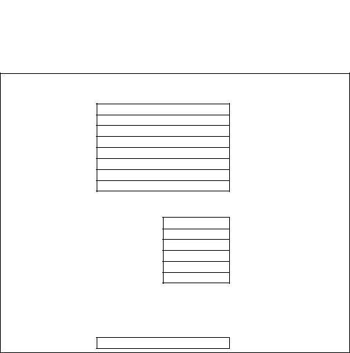
The processor provides 16 basic program execution registers for use in general system and application programing (see Figure 3-4). These registers can be grouped as follows:
•General-purpose registers. These eight registers are available for storing operands and pointers.
•Segment registers. These registers hold up to six segment selectors.
•EFLAGS (program status and control) register. The EFLAGS register report on the status of the program being executed and allows limited (application-program level) control of the processor.
•EIP (instruction pointer) register. The EIP register contains a 32-bit pointer to the next instruction to be executed.
3.4.1General-Purpose Registers
The 32-bit general-purpose registers EAX, EBX, ECX, EDX, ESI, EDI, EBP, and ESP are provided for holding the following items:
•
•
•
Operands for logical and arithmetic operations Operands for address calculations
Memory pointers
Although all of these registers are available for general storage of operands, results, and pointers, caution should be used when referencing the ESP register. The ESP register holds the stack pointer and as a general rule should not be used for another purpose.
Many instructions assign specific registers to hold operands. For example, string instructions use the contents of the ECX, ESI, and EDI registers as operands. When using a segmented memory model, some instructions assume that pointers in certain registers are relative to
Vol. 1 3-13
BASIC EXECUTION ENVIRONMENT
specific segments. For instance, some instructions assume that a pointer in the EBX register points to a memory location in the DS segment.
31 |
General-Purpose Registers |
0 |
|
EAX
EBX
ECX
EDX
ESI
EDI
EBP
ESP
Segment Registers
15 |
0 |
CS
DS
SS
ES
FS
GS
Program Status and Control Register
31 |
|
0 |
|
|
|
|
EFLAGS |
31 |
Instruction Pointer |
0 |
|
|
|
EIP
Figure 3-4. General System and Application Programming Registers
The special uses of general-purpose registers by instructions are described in Chapter 5, “Instruction Set Summary” in this volume; see also Chapter 3, Instruction Set Reference A-M and Chapter 4, Instruction Set Reference N-Z of the IA-32 Intel Architecture Software Developer’s Manual, Volumes 2A & 2B. The following is a summary of special uses:
•EAX — Accumulator for operands and results data
•EBX — Pointer to data in the DS segment
•ECX — Counter for string and loop operations
•EDX — I/O pointer
•ESI — Pointer to data in the segment pointed to by the DS register; source pointer for string operations
3-14 Vol. 1
BASIC EXECUTION ENVIRONMENT
•EDI — Pointer to data (or destination) in the segment pointed to by the ES register; destination pointer for string operations
•ESP — Stack pointer (in the SS segment)
•EBP — Pointer to data on the stack (in the SS segment)
As shown in Figure 3-5, the lower 16 bits of the general-purpose registers map directly to the register set found in the 8086 and Intel 286 processors and can be referenced with the names AX, BX, CX, DX, BP, SI, DI, and SP. Each of the lower two bytes of the EAX, EBX, ECX, and EDX registers can be referenced by the names AH, BH, CH, and DH (high bytes) and AL, BL, CL, and DL (low bytes).
|
|
General-Purpose Registers |
0 16-bit 32-bit |
|||||
|
31 |
16 15 |
8 7 |
|||||
|
|
|
AH |
|
AL |
|
AX |
EAX |
|
|
|
BH |
|
BL |
|
BX |
EBX |
|
|
|
CH |
|
CL |
|
CX |
ECX |
|
|
|
DH |
|
DL |
|
DX |
EDX |
|
|
|
|
BP |
|
|
EBP |
|
|
|
|
|
SI |
|
|
ESI |
|
|
|
|
|
DI |
|
|
EDI |
|
|
|
|
|
SP |
|
|
ESP |
|
|
|
|
|
|
|
|
|
|
Figure 3-5. Alternate General-Purpose Register Names
3.4.1.1General-Purpose Registers in 64-Bit Mode
In 64-bit mode, there are 16 general purpose registers and the default operand size is 32 bits. However, general-purpose registers are able to work with either 32-bit or 64-bit operands. If a 32-bit operand size is specified: EAX, EBX, ECX, EDX, EDI, ESI, EBP, ESP, R8D - R15D are available. If a 64-bit operand size is specified: RAX, RBX, RCX, RDX, RDI, RSI, RBP, RSP, R8-R15 are available. R8D-R15D/R8-R15 represent eight new general-purpose registers. All of these registers can be accessed at the byte, word, dword, and qword level. REX prefixes are used to generate 64-bit operand sizes or to reference registers R8-R15.
Vol. 1 3-15