


GUIDELINES FOR WRITING X87 FPU EXCEPTION HANDLERS
The Intel386 processor and its companion Intel 387 numeric coprocessor provided the same hardware mechanism for signaling and handling floating-point exceptions as the Intel 286 and 287 processors. And again, to maintain compatibility with existing MS-DOS software, basically the same MS-DOS compatibility floating-point exception handling mechanism that was used in the IBM PC AT was used in PCs based on the Intel386 processor.
D.2 IMPLEMENTATION OF THE MS-DOS COMPATIBILITY SUB-MODE IN THE INTEL486, PENTIUM, AND P6 PROCESSOR FAMILY, AND PENTIUM 4 PROCESSORS
Beginning with the Intel486 processor, the IA-32 architecture provided a dedicated mechanism for enabling the MS-DOS compatibility mode for x87 FPU exceptions and for generating external x87 FPU-exception signals while operating in this mode. The following sections describe the implementation of the MS-DOS compatibility mode in the Intel486 and Pentium processors and in the P6 family and Pentium 4 processors. Also described is the recommended external hardware to support this mode of operation.
D.2.1 MS-DOS Compatibility Sub-mode in the Intel486 and
Pentium Processors
In the Intel486 processor, several things were done to enhance and speed up the numeric coprocessor, now called the floating-point unit (x87 FPU). The most important enhancement was that the x87 FPU was included in the same chip as the processor, for increased speed in x87 FPU computations and reduced latency for x87 FPU exception handling. Also, for the first time, the MS-DOS compatibility mode was built into the chip design, with the addition of the NE bit in control register CR0 and the addition of the FERR# (Floating-point ERRor) and IGNNE# (IGNore Numeric Error) pins.
The NE bit selects the native x87 FPU exception handling mode (NE = 1) or the MS-DOS compatibility mode (NE = 0). When native mode is selected, all signaling of floating-point exceptions is handled internally in the Intel486 chip, resulting in the generation of an interrupt 16.
When MS-DOS compatibility mode is selected, the FERRR# and IGNNE# pins are used to signal floating-point exceptions. The FERR# output pin, which replaces the ERROR# pin from the previous generations of IA-32 numeric coprocessors, is connected to a PIC. A new input signal, IGNNE#, is provided to allow the x87 FPU exception handler to execute x87 FPU instructions, if desired, without first clearing the error condition and without triggering the interrupt a second time. This IGNNE# feature is needed to replicate the capability that was provided on MS-DOS compatible Intel 286 and Intel 287 and Intel386 and Intel 387 systems by turning off the BUSY# signal, when inside the x87 FPU exception handler, before clearing the error condition.
Note that Intel, in order to provide Intel486 processors for market segments that had no need for an x87 FPU, created the “SX” versions. These Intel486 SX processors did not contain the float- ing-point unit. Intel also produced Intel 487 SX processors for end users who later decided to
Vol. 1 D-3

GUIDELINES FOR WRITING X87 FPU EXCEPTION HANDLERS
upgrade to a system with an x87 FPU. These Intel 487 SX processors are similar to standard Intel486 processors with a working x87 FPU on board.
Thus, the external circuitry necessary to support the MS-DOS compatibility mode for Intel 487 SX processors is the same as for standard Intel486 DX processors.
The Pentium, P6 family, and Pentium 4 processors offer the same mechanism (the NE bit and the FERR# and IGNNE# pins) as the Intel486 processors for generating x87 FPU exceptions in MS-DOS compatibility mode. The actions of these mechanisms are slightly different and more straightforward for the P6 family and Pentium 4 processors, as described in Section D.2.2, “MS-DOS Compatibility Sub-mode in the P6 Family and Pentium 4 Processors”.
For Pentium, P6 family, and Pentium 4 processors, it is important to note that the special DP (Dual Processing) mode for Pentium processors and also the more general Intel MultiProcessor Specification for systems with multiple Pentium, P6 family, or Pentium 4 processors support x87 FPU exception handling only in the native mode. Intel does not recommend using the MS-DOS compatibility x87 FPU mode for systems using more than one processor.
D.2.1.1 Basic Rules: When FERR# Is Generated
When MS-DOS compatibility mode is enabled for the Intel486 or Pentium processors (NE bit is set to 0) and the IGNNE# input pin is de-asserted, the FERR# signal is generated as follows:
1.When an x87 FPU instruction causes an unmasked x87 FPU exception, the processor (in most cases) uses a “deferred” method of reporting the error. This means that the processor does not respond immediately, but rather freezes just before executing the next WAIT or x87 FPU instruction (except for “no-wait” instructions, which the x87 FPU executes regardless of an error condition).
2.When the processor freezes, it also asserts the FERR# output.
3.The frozen processor waits for an external interrupt, which must be supplied by external hardware in response to the FERR# assertion.
4.In MS-DOS* compatibility systems, FERR# is fed to the IRQ13 input in the cascaded PIC. The PIC generates interrupt 75H, which then branches to interrupt 2, as described earlier in this appendix for systems using the Intel 286 and Intel 287 or Intel386 and Intel 387 processors.
The deferred method of error reporting is used for all exceptions caused by the basic arithmetic instructions (including FADD, FSUB, FMUL, FDIV, FSQRT, FCOM and FUCOM), for precision exceptions caused by all types of x87 FPU instructions, and for numeric underflow and overflow exceptions caused by all types of x87 FPU instructions except stores to memory.
Some x87 FPU instructions with some x87 FPU exceptions use an “immediate” method of reporting errors. Here, the FERR# is asserted immediately, at the time that the exception occurs. The immediate method of error reporting is used for x87 FPU stack fault, invalid operation and denormal exceptions caused by all transcendental instructions, FSCALE, FXTRACT, FPREM and others, and all exceptions (except precision) when caused by x87 FPU store instructions. Like deferred error reporting, immediate error reporting will cause the processor to freeze just
D-4 Vol. 1

GUIDELINES FOR WRITING X87 FPU EXCEPTION HANDLERS
before executing the next WAIT or x87 FPU instruction if the error condition has not been cleared by that time.
Note that in general, whether deferred or immediate error reporting is used for an x87 FPU exception depends both on which exception occurred and which instruction caused that exception. A complete specification of these cases, which applies to both the Pentium and the Intel486 processors, is given in Section 5.1.21 in the Pentium Processor Family Developer’s Manual: Volume 1.
If NE = 0 but the IGNNE# input is active while an unmasked x87 FPU exception is in effect, the processor disregards the exception, does not assert FERR#, and continues. If IGNNE# is then de-asserted and the x87 FPU exception has not been cleared, the processor will respond as described above. (That is, an immediate exception case will assert FERR# immediately. A deferred exception case will assert FERR# and freeze just before the next x87 FPU or WAIT instruction.) The assertion of IGNNE# is intended for use only inside the x87 FPU exception handler, where it is needed if one wants to execute non-control x87 FPU instructions for diagnosis, before clearing the exception condition. When IGNNE# is asserted inside the exception handler, a preceding x87 FPU exception has already caused FERR# to be asserted, and the external interrupt hardware has responded, but IGNNE# assertion still prevents the freeze at x87 FPU instructions. Note that if IGNNE# is left active outside of the x87 FPU exception handler, additional x87 FPU instructions may be executed after a given instruction has caused an x87 FPU exception. In this case, if the x87 FPU exception handler ever did get invoked, it could not determine which instruction caused the exception.
To properly manage the interface between the processor’s FERR# output, its IGNNE# input, and the IRQ13 input of the PIC, additional external hardware is needed. A recommended configuration is described in the following section.
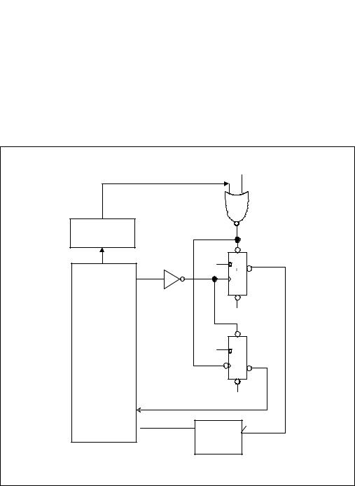
D.2.1.2 Recommended External Hardware to Support the MS-DOS Compatibility Sub-mode
Figure D-1 provides an external circuit that will assure proper handling of FERR# and IGNNE# when an x87 FPU exception occurs. In particular, it assures that IGNNE# will be active only inside the x87 FPU exception handler without depending on the order of actions by the exception handler. Some hardware implementations have been less robust because they have depended on the exception handler to clear the x87 FPU exception interrupt request to the PIC (FP_IRQ signal) before the handler causes FERR# to be de-asserted by clearing the exception from the x87 FPU itself. Figure D-2 shows the details of how IGNNE# will behave when the circuit in Figure D-1 is implemented. The temporal regions within the x87 FPU exception handler activity are described as follows:
1.The FERR# signal is activated by an x87 FPU exception and sends an interrupt request through the PIC to the processor’s INTR pin.
2.During the x87 FPU interrupt service routine (exception handler) the processor will need to clear the interrupt request latch (Flip Flop #1). It may also want to execute non-control x87 FPU instructions before the exception is cleared from the x87 FPU. For this purpose the IGNNE# must be driven low. Typically in the PC environment an I/O access to Port 0F0H clears the external x87 FPU exception interrupt request (FP_IRQ). In the
Vol. 1 D-5
 ,175
,175 