- •CONTENTS
- •1.2 Overview of Volume 1: Basic Architecture
- •1.3 Notational Conventions
- •1.3.1 Bit and Byte Order
- •1.3.2 Reserved Bits and Software Compatibility
- •1.3.3 Instruction Operands
- •1.3.4 Hexadecimal and Binary Numbers
- •1.3.5 Segmented Addressing
- •1.3.6 A New Syntax for CPUID, CR, and MSR Values
- •1.3.7 Exceptions
- •1.4 Related Literature
- •2.1.10 The Intel Pentium Processor Extreme Edition (2005)
- •2.2 More on SPECIFIC advances
- •2.2.1 P6 Family Microarchitecture
- •2.2.2.1 The Front End Pipeline
- •2.2.2.3 Retirement Unit
- •2.2.3 SIMD Instructions
- •2.2.4 Hyper-Threading Technology
- •2.2.4.1 Some Implementation Notes
- •3.1 Modes of Operation
- •3.2 Overview of the Basic Execution Environment
- •3.3 Memory Organization
- •3.3.1 Three Memory Models
- •3.3.2 Paging and Virtual Memory
- •3.3.4 Modes of Operation vs. Memory Model
- •3.3.6 Extended Physical Addressing in Protected Mode
- •3.3.7.1 Canonical Addressing
- •3.4 Basic Program Execution Registers
- •3.4.2 Segment Registers
- •3.4.3 EFLAGS Register
- •3.4.3.1 Status Flags
- •3.4.3.2 DF Flag
- •3.4.3.3 System Flags and IOPL Field
- •3.5 Instruction Pointer
- •3.7 Operand Addressing
- •3.7.1 Immediate Operands
- •3.7.2 Register Operands
- •3.7.3 Memory Operands
- •3.7.4 Specifying a Segment Selector
- •3.7.5 Specifying an Offset
- •3.7.6 Assembler and Compiler Addressing Modes
- •3.7.7 I/O Port Addressing
- •4.1 Fundamental Data Types
- •4.1.1 Alignment of Words, Doublewords, Quadwords, and Double Quadwords
- •4.2 Numeric Data Types
- •4.2.1 Integers
- •4.2.1.1 Unsigned Integers
- •4.2.1.2 Signed Integers
- •4.3 Pointer Data Types
- •4.4 Bit Field Data Type
- •4.5 String Data Types
- •4.6 Packed SIMD Data Types
- •4.6.2 128-Bit Packed SIMD Data Types
- •4.7 BCD and Packed BCD Integers
- •4.8.1 Real Number System
- •4.8.2.1 Normalized Numbers
- •4.8.2.2 Biased Exponent
- •4.8.3.1 Signed Zeros
- •4.8.3.2 Normalized and Denormalized Finite Numbers
- •4.8.3.3 Signed Infinities
- •4.8.3.4 NaNs
- •4.8.3.5 Operating on SNaNs and QNaNs
- •4.8.3.6 Using SNaNs and QNaNs in Applications
- •4.8.4 Rounding
- •4.8.4.1 Rounding Control (RC) Fields
- •4.8.4.2 Truncation with SSE and SSE2 Conversion Instructions
- •4.9.1.1 Invalid Operation Exception (#I)
- •4.9.1.2 Denormal Operand Exception (#D)
- •4.9.1.4 Numeric Overflow Exception (#O)
- •4.9.1.5 Numeric Underflow Exception (#U)
- •5.1.1 Data Transfer Instructions
- •5.1.2 Binary Arithmetic Instructions
- •5.1.3 Decimal Arithmetic Instructions
- •5.1.4 Logical Instructions
- •5.1.5 Shift and Rotate Instructions
- •5.1.6 Bit and Byte Instructions
- •5.1.7 Control Transfer Instructions
- •5.1.8 String Instructions
- •5.1.9 I/O Instructions
- •5.1.10 Enter and Leave Instructions
- •5.1.11 Flag Control (EFLAG) Instructions
- •5.1.12 Segment Register Instructions
- •5.1.13 Miscellaneous Instructions
- •5.2 x87 FPU Instructions
- •5.2.1 x87 FPU Data Transfer Instructions
- •5.2.2 x87 FPU Basic Arithmetic Instructions
- •5.2.3 x87 FPU Comparison Instructions
- •5.2.4 x87 FPU Transcendental Instructions
- •5.2.5 x87 FPU Load Constants Instructions
- •5.2.6 x87 FPU Control Instructions
- •5.3 x87 FPU AND SIMD State Management Instructions
- •5.4.1 MMX Data Transfer Instructions
- •5.4.2 MMX Conversion Instructions
- •5.4.3 MMX Packed Arithmetic Instructions
- •5.4.4 MMX Comparison Instructions
- •5.4.5 MMX Logical Instructions
- •5.4.6 MMX Shift and Rotate Instructions
- •5.4.7 MMX State Management Instructions
- •5.5 SSE Instructions
- •5.5.1.1 SSE Data Transfer Instructions
- •5.5.1.2 SSE Packed Arithmetic Instructions
- •5.5.1.3 SSE Comparison Instructions
- •5.5.1.4 SSE Logical Instructions
- •5.5.1.5 SSE Shuffle and Unpack Instructions
- •5.5.1.6 SSE Conversion Instructions
- •5.5.2 SSE MXCSR State Management Instructions
- •5.5.4 SSE Cacheability Control, Prefetch, and Instruction Ordering Instructions
- •5.6 SSE2 Instructions
- •5.6.1.1 SSE2 Data Movement Instructions
- •5.6.1.2 SSE2 Packed Arithmetic Instructions
- •5.6.1.3 SSE2 Logical Instructions
- •5.6.1.4 SSE2 Compare Instructions
- •5.6.1.5 SSE2 Shuffle and Unpack Instructions
- •5.6.1.6 SSE2 Conversion Instructions
- •5.6.4 SSE2 Cacheability Control and Ordering Instructions
- •5.7 SSE3 Instructions
- •5.7.6 SSE3 Agent Synchronization Instructions
- •5.8 System Instructions
- •CHAPTER 6 Procedure Calls, Interrupts, and Exceptions
- •6.1 Procedure Call Types
- •6.2 Stacks
- •6.2.1 Setting Up a Stack
- •6.2.2 Stack Alignment
- •6.2.4 Procedure Linking Information
- •6.2.4.2 Return Instruction Pointer
- •6.3 Calling Procedures Using CALL and RET
- •6.3.1 Near CALL and RET Operation
- •6.3.2 Far CALL and RET Operation
- •6.3.3 Parameter Passing
- •6.3.3.2 Passing Parameters on the Stack
- •6.3.3.3 Passing Parameters in an Argument List
- •6.3.4 Saving Procedure State Information
- •6.3.5 Calls to Other Privilege Levels
- •6.3.6 CALL and RET Operation Between Privilege Levels
- •6.4 Interrupts and Exceptions
- •6.4.1 Call and Return Operation for Interrupt or Exception Handling Procedures
- •6.4.2 Calls to Interrupt or Exception Handler Tasks
- •6.5.1 ENTER Instruction
- •6.5.2 LEAVE Instruction
- •CHAPTER 7 Programming With General-Purpose Instructions
- •7.1 Programming environment for gp Instructions
- •7.3 Summary of gp Instructions
- •7.3.1. Data Transfer Instructions
- •7.3.1.1 General Data Movement Instructions
- •7.3.1.2 Exchange Instructions
- •7.3.1.4 Stack Manipulation Instructions
- •7.3.1.6 Type Conversion Instructions
- •7.3.2. Binary Arithmetic Instructions
- •7.3.2.1 Addition and Subtraction Instructions
- •7.3.2.2 Increment and Decrement Instructions
- •7.3.2.4 Comparison and Sign Change Instruction
- •7.3.2.5 Multiplication and Divide Instructions
- •7.3.3. Decimal Arithmetic Instructions
- •7.3.3.1 Packed BCD Adjustment Instructions
- •7.3.3.2 Unpacked BCD Adjustment Instructions
- •7.3.5. Logical Instructions
- •7.3.6. Shift and Rotate Instructions
- •7.3.6.1 Shift Instructions
- •7.3.6.3 Rotate Instructions
- •7.3.7. Bit and Byte Instructions
- •7.3.7.1 Bit Test and Modify Instructions
- •7.3.7.2 Bit Scan Instructions
- •7.3.7.3 Byte Set on Condition Instructions
- •7.3.7.4 Test Instruction
- •7.3.8. Control Transfer Instructions
- •7.3.8.1 Unconditional Transfer Instructions
- •7.3.8.2 Conditional Transfer Instructions
- •7.3.8.4 Software Interrupt Instructions
- •7.3.9. String Operations
- •7.3.9.1 Repeating String Operations
- •7.3.10. String Operations in 64-Bit Mode
- •7.3.11. I/O Instructions
- •7.3.12. I/O Instructions in 64-Bit Mode
- •7.3.13. Enter and Leave Instructions
- •7.3.14. Flag Control (EFLAG) Instructions
- •7.3.14.1 Carry and Direction Flag Instructions
- •7.3.14.2 EFLAGS Transfer Instructions
- •7.3.14.3 Interrupt Flag Instructions
- •7.3.15. Flag Control (RFLAG) Instructions in 64-Bit Mode
- •7.3.16. Segment Register Instructions
- •7.3.16.2 Far Control Transfer Instructions
- •7.3.16.3 Software Interrupt Instructions
- •7.3.16.4 Load Far Pointer Instructions
- •7.3.17. Miscellaneous Instructions
- •7.3.17.1 Address Computation Instruction
- •7.3.17.2 Table Lookup Instructions
- •7.3.17.3 Processor Identification Instruction
- •8.1 x87 FPU Execution Environment
- •8.1.2 x87 FPU Data Registers
- •8.1.2.1 Parameter Passing With the x87 FPU Register Stack
- •8.1.3 x87 FPU Status Register
- •8.1.3.1 Top of Stack (TOP) Pointer
- •8.1.3.2 Condition Code Flags
- •8.1.3.4 Stack Fault Flag
- •8.1.4 Branching and Conditional Moves on Condition Codes
- •8.1.5 x87 FPU Control Word
- •8.1.5.2 Precision Control Field
- •8.1.5.3 Rounding Control Field
- •8.1.6 Infinity Control Flag
- •8.1.7 x87 FPU Tag Word
- •8.1.8 x87 FPU Instruction and Data (Operand) Pointers
- •8.1.9 Last Instruction Opcode
- •8.1.10 Saving the x87 FPU’s State with FSTENV/FNSTENV and FSAVE/FNSAVE
- •8.1.11 Saving the x87 FPU’s State with FXSAVE
- •8.2 x87 FPU Data Types
- •8.2.1 Indefinites
- •8.3 x86 FPU Instruction Set
- •8.3.1 Escape (ESC) Instructions
- •8.3.2 x87 FPU Instruction Operands
- •8.3.3 Data Transfer Instructions
- •8.3.4 Load Constant Instructions
- •8.3.5 Basic Arithmetic Instructions
- •8.3.6 Comparison and Classification Instructions
- •8.3.6.1 Branching on the x87 FPU Condition Codes
- •8.3.7 Trigonometric Instructions
- •8.3.9 Logarithmic, Exponential, and Scale
- •8.3.10 Transcendental Instruction Accuracy
- •8.3.11 x87 FPU Control Instructions
- •8.3.13 Unsupported x87 FPU Instructions
- •8.5.1 Invalid Operation Exception
- •8.5.1.1 Stack Overflow or Underflow Exception (#IS)
- •8.5.1.2 Invalid Arithmetic Operand Exception (#IA)
- •8.5.2 Denormal Operand Exception (#D)
- •8.5.4 Numeric Overflow Exception (#O)
- •8.5.5 Numeric Underflow Exception (#U)
- •8.6 x87 FPU Exception Synchronization
- •8.7 Handling x87 FPU Exceptions in Software
- •8.7.1 Native Mode
- •8.7.3 Handling x87 FPU Exceptions in Software
- •9.1 Overview of MMX Technology
- •9.2 The MMX Technology Programming Environment
- •9.2.2 MMX Registers
- •9.2.3 MMX Data Types
- •9.2.4 Memory Data Formats
- •9.2.5 Single Instruction, Multiple Data (SIMD) Execution Model
- •9.3 Saturation and Wraparound Modes
- •9.4 MMX Instructions
- •9.4.1 Data Transfer Instructions
- •9.4.2 Arithmetic Instructions
- •9.4.3 Comparison Instructions
- •9.4.4 Conversion Instructions
- •9.4.5 Unpack Instructions
- •9.4.6 Logical Instructions
- •9.4.7 Shift Instructions
- •9.4.8 EMMS Instruction
- •9.5 Compatibility with x87 FPU Architecture
- •9.5.1 MMX Instructions and the x87 FPU Tag Word
- •9.6 WRITING APPLICATIONS WITH MMX CODE
- •9.6.1 Checking for MMX Technology Support
- •9.6.2 Transitions Between x87 FPU and MMX Code
- •9.6.3 Using the EMMS Instruction
- •9.6.4 Mixing MMX and x87 FPU Instructions
- •9.6.5 Interfacing with MMX Code
- •9.6.6 Using MMX Code in a Multitasking Operating System Environment
- •9.6.7 Exception Handling in MMX Code
- •9.6.8 Register Mapping
- •9.6.9 Effect of Instruction Prefixes on MMX Instructions
- •CHAPTER 10 Programming with Streaming SIMD Extensions (SSE)
- •10.1 Overview of SSE Extensions
- •10.2 SSE Programming Environment
- •10.2.2 XMM Registers
- •10.2.3 MXCSR Control and Status Register
- •10.2.3.3 Flush-To-Zero
- •10.2.3.4 Denormals-Are-Zeros
- •10.2.4 Compatibility of SSE Extensions with SSE2/SSE3/MMX and the x87 FPU
- •10.3 SSE Data Types
- •10.4 SSE Instruction Set
- •10.4.1.1 SSE Data Movement Instructions
- •10.4.1.2 SSE Arithmetic Instructions
- •10.4.2 SSE Logical Instructions
- •10.4.2.1 SSE Comparison Instructions
- •10.4.2.2 SSE Shuffle and Unpack Instructions
- •10.4.3 SSE Conversion Instructions
- •10.4.5 MXCSR State Management Instructions
- •10.4.6 Cacheability Control, Prefetch, and Memory Ordering Instructions
- •10.4.6.1 Cacheability Control Instructions
- •10.4.6.4 SFENCE Instruction
- •10.5 FXSAVE and FXRSTOR Instructions
- •10.6 Handling SSE Instruction Exceptions
- •10.7 Writing Applications with the SSE Extensions
- •CHAPTER 11 Programming with Streaming SIMD Extensions 2 (SSE2)
- •11.1 Overview of SSE2 Extensions
- •11.2 SSE2 Programming Environment
- •11.2.2 Compatibility of SSE2 Extensions with SSE, MMX Technology and x87 FPU Programming Environment
- •11.3 SSE2 Data Types
- •11.4 SSE2 Instructions
- •11.4.1.1 Data Movement Instructions
- •11.4.1.2 SSE2 Arithmetic Instructions
- •11.4.1.3 SSE2 Logical Instructions
- •11.4.1.4 SSE2 Comparison Instructions
- •11.4.1.5 SSE2 Shuffle and Unpack Instructions
- •11.4.1.6 SSE2 Conversion Instructions
- •11.4.4 Cacheability Control and Memory Ordering Instructions
- •11.4.4.1 FLUSH Cache Line
- •11.4.4.2 Cacheability Control Instructions
- •11.4.4.3 Memory Ordering Instructions
- •11.4.4.4 Pause
- •11.4.5 Branch Hints
- •11.5 SSE, SSE2, and SSE3 Exceptions
- •11.5.1 SIMD Floating-Point Exceptions
- •11.5.2.1 Invalid Operation Exception (#I)
- •11.5.2.4 Numeric Overflow Exception (#O)
- •11.5.2.5 Numeric Underflow Exception (#U)
- •11.5.3.1 Handling Masked Exceptions
- •11.5.3.2 Handling Unmasked Exceptions
- •11.5.3.3 Handling Combinations of Masked and Unmasked Exceptions
- •11.6 Writing Applications with SSE/SSE2 Extensions
- •11.6.1 General Guidelines for Using SSE/SSE2 Extensions
- •11.6.2 Checking for SSE/SSE2 Support
- •11.6.3 Checking for the DAZ Flag in the MXCSR Register
- •11.6.4 Initialization of SSE/SE2 Extensions
- •11.6.5 Saving and Restoring the SSE/SSE2 State
- •11.6.6 Guidelines for Writing to the MXCSR Register
- •11.6.7 Interaction of SSE/SSE2 Instructions with x87 FPU and MMX Instructions
- •11.6.10 Interfacing with SSE/SSE2 Procedures and Functions
- •11.6.10.1 Passing Parameters in XMM Registers
- •11.6.10.2 Saving XMM Register State on a Procedure or Function Call
- •11.6.12 Branching on Arithmetic Operations
- •11.6.13 Cacheability Hint Instructions
- •11.6.14 Effect of Instruction Prefixes on the SSE/SSE2 Instructions
- •CHAPTER 12 Programming with Streaming SIMD Extensions 3 (SSE3)
- •12.1 Overview of SSE3 Instructions
- •12.2 SSE3 Programming Environment and Data types
- •12.2.2 Compatibility of SSE3 Extensions with MMX Technology, the x87 FPU Environment, and SSE/SSE2 Extensions
- •12.2.3 Horizontal and Asymmetric Processing
- •12.3 SSE3 Instructions
- •12.3.1 x87 FPU Instruction for Integer Conversion
- •12.3.6 Two Thread Synchronization Instructions
- •12.4 SSE3 Exceptions
- •12.4.1 Device Not Available (DNA) Exceptions
- •12.4.2 Numeric Error flag and IGNNE#
- •12.4.3 Emulation
- •12.5 Writing Applications with SSE3 Extensions
- •12.5.1 General Guidelines for Using SSE3 Extensions
- •12.5.2 Checking for SSE3 Support
- •12.5.4 Programming SSE3 with SSE/SSE2 Extensions
- •13.1 I/O Port Addressing
- •13.2 I/O Port Hardware
- •13.3 I/O Address Space
- •13.4 I/O Instructions
- •13.5.1 I/O Privilege Level
- •13.5.2 I/O Permission Bit Map
- •13.6 Ordering I/O
- •CHAPTER 14 Processor Identification and Feature Determination
- •14.1 Using the CPUID Instruction
- •14.1.1 Notes on Where to Start
- •A.1 EFLAGS and Instructions
- •B.1 Condition Codes
- •APPENDIX C Floating-Point Exceptions Summary
- •C.1 Overview
- •C.2 x87 FPU Instructions
- •C.3 SSE Instructions
- •C.4 SSE2 Instructions
- •C.5 SSE3 Instructions
- •D.1 Origin of the MS-DOS Compatibility Sub-mode for Handling x87 FPU Exceptions
- •D.2 Implementation of the MS-DOS Compatibility Sub-mode In the Intel486, Pentium, AND P6 Processor Family, and Pentium 4 Processors
- •D.2.1.1 Basic Rules: When FERR# Is Generated
- •D.2.1.2 Recommended External Hardware to Support the MS-DOS Compatibility Sub-mode
- •D.2.1.3 No-Wait x87 FPU Instructions Can Get x87 FPU Interrupt in Window
- •D.2.2 MS-DOS Compatibility Sub-mode in the P6 Family and Pentium 4 Processors
- •D.3 Recommended Protocol for MS-DOS* Compatibility Handlers
- •D.3.1 Floating-Point Exceptions and Their Defaults
- •D.3.2 Two Options for Handling Numeric Exceptions
- •D.3.2.1 Automatic Exception Handling: Using Masked Exceptions
- •D.3.2.2 Software Exception Handling
- •D.3.3 Synchronization Required for Use of x87 FPU Exception Handlers
- •D.3.3.1 Exception Synchronization: What, Why and When
- •D.3.3.2 Exception Synchronization Examples
- •D.3.3.3 Proper Exception Synchronization
- •D.3.4 x87 FPU Exception Handling Examples
- •D.3.6 Considerations When x87 FPU Shared Between Tasks
- •D.3.6.1 Speculatively Deferring x87 FPU Saves, General Overview
- •D.3.6.2 Tracking x87 FPU Ownership
- •D.3.6.4 Interrupt Routing From the Kernel
- •D.3.6.5 Special Considerations for Operating Systems that Support Streaming SIMD Extensions
- •D.4 Differences For Handlers Using Native Mode
- •D.4.1 Origin with the Intel 286 and Intel 287, and Intel386 and Intel 387 Processors
- •D.4.2 Changes with Intel486, Pentium and Pentium Pro Processors with CR0.NE[bit 5] = 1
- •D.4.3 Considerations When x87 FPU Shared Between Tasks Using Native Mode
- •APPENDIX E Guidelines for Writing SIMD Floating-Point Exception Handlers
- •E.1 Two Options for Handling Floating-Point Exceptions
- •E.2 Software Exception Handling
- •E.3 Exception Synchronization
- •E.4 SIMD Floating-Point Exceptions and the IEEE Standard 754
- •E.4.1 Floating-Point Emulation
- •E.4.2 SSE/SSE2/SSE3 Response To Floating-Point Exceptions
- •E.4.2.1 Numeric Exceptions
- •E.4.2.2 Results of Operations with NaN Operands or a NaN Result for SSE/SSE2/SSE3 Numeric Instructions
- •E.4.2.3 Condition Codes, Exception Flags, and Response for Masked and Unmasked Numeric Exceptions
- •E.4.3 Example SIMD Floating-Point Emulation Implementation
- •INDEX
- •INTEL SALES OFFICES
BASIC EXECUTION ENVIRONMENT
Table 3-2. Addressable General Purpose Registers
Register Type |
Without REX |
With REX |
|
|
|
Byte Registers |
AL, BL, CL, DL, AH, BH, CH, |
AL, BL, CL, DL, DIL, SIL, BPL, SPL, |
|
DH |
R8L - R15L |
|
|
|
Word Registers |
AX, BX, CX, DX, DI, SI, BP, |
AX, BX, CX, DX, DI, SI, BP, SP, |
|
SP |
R8W - R15W |
|
|
|
Doubleword Registers |
EAX, EBX, ECX, EDX, EDI, |
EAX, EBX, ECX, EDX, EDI, ESI, |
|
ESI, EBP, ESP |
EBP, ESP, R8D - R15D |
|
|
|
Quadword Registers |
N.A. |
RAX, RBX, RCX, RDX, RDI, RSI, |
|
|
RBP, RSP, R8 - R15 |
|
|
|
In 64-bit mode, there are limitations on accessing byte registers. An instruction cannot reference legacy high-bytes (for example: AH, BH, CH, DH) and one of the new byte registers at the same time (for example: the low byte of the RAX register). However, instructions may reference legacy low-bytes (for example: AL, BL, CL or DL) and new byte registers at the same time (for example: the low byte of the R8 register, or RBP). The architecture enforces this limitation by changing high-byte references (AH, BH, CH, DH) to low byte references (BPL, SPL, DIL, SIL: the low 8 bits for RBP, RSP, RDI and RSI) for instructions using an REX prefix.
When in 64-bit mode, operand size determines the number of valid bits in the destination general-purpose register:
•64-bit operands generate a 64-bit result in the destination general-purpose register.
•32-bit operands generate a 32-bit result, zero-extended to a 64-bit result in the destination general-purpose register.
•8-bit and 16-bit operands generate an 8-bit or 16-bit result. The upper 56 bits or 48 bits (respectively) of the destination general-purpose register are not be modified by the operation. If the result of an 8-bit or 16-bit operation is intended for 64-bit address calculation, explicitly sign-extend the register to the full 64-bits.
Because the upper 32 bits of 64-bit general-purpose registers are undefined in 32-bit modes, the upper 32 bits of any general-purpose register are not preserved when switching from 64-bit mode to a 32-bit mode (to protected mode or compatibility mode). Software must not depend on these bits to maintain a value after a 64-bit to 32-bit mode switch.
3.4.2Segment Registers
The segment registers (CS, DS, SS, ES, FS, and GS) hold 16-bit segment selectors. A segment selector is a special pointer that identifies a segment in memory. To access a particular segment in memory, the segment selector for that segment must be present in the appropriate segment register.
When writing application code, programmers generally create segment selectors with assembler directives and symbols. The assembler and other tools then create the actual segment selector values associated with these directives and symbols. If writing system code, programmers may
3-16 Vol. 1
BASIC EXECUTION ENVIRONMENT
need to create segment selectors directly. A detailed description of the segment-selector data structure is given in Chapter 3, Protected-Mode Memory Management, of the IA-32 Intel Architecture Software Developer’s Manual, Volume 3.
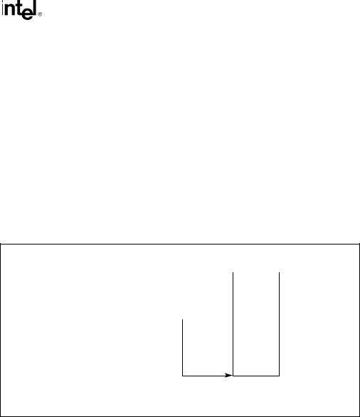
How segment registers are used depends on the type of memory management model that the operating system or executive is using. When using the flat (unsegmented) memory model, segment registers are loaded with segment selectors that point to overlapping segments, each of which begins at address 0 of the linear address space (see Figure 3-6). These overlapping segments then comprise the linear address space for the program. Typically, two overlapping segments are defined: one for code and another for data and stacks. The CS segment register points to the code segment and all the other segment registers point to the data and stack segment.
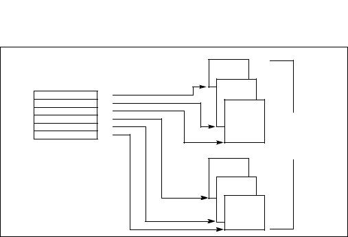
When using the segmented memory model, each segment register is ordinarily loaded with a different segment selector so that each segment register points to a different segment within the linear address space (see Figure 3-7). At any time, a program can thus access up to six segments in the linear address space. To access a segment not pointed to by one of the segment registers, a program must first load the segment selector for the segment to be accessed into a segment register.
|
|
|
|
|
Linear Address |
||
|
|
|
|
|
Space for Program |
||
Segment Registers |
|
|
|
|
|
Overlapping |
|
|
|
|
|
|
|
Segments |
|
|
CS |
|
|
of up to |
|||
|
|||||||
|
|
|
4 GBytes |
||||
|
DS |
|
|
||||
|
|
|
Beginning at |
||||
|
SS |
|
|
|
|||
|
|
|
|
||||
|
|
|
|
Address 0 |
|||
|
ES |
|
|
|
|
||
|
|
|
|
|
|||
|
|
|
|
|
|
||
|
FS |
|
|
|
|
||
|
|
|
|
|
|||
|
GS |
|
|
|
|
||
|
|
|
|
|
The segment selector in each segment register points to an overlapping
segment in the linear address space.
Figure 3-6. Use of Segment Registers for Flat Memory Model
Vol. 1 3-17
BASIC EXECUTION ENVIRONMENT
|
Code |
|
Segment Registers |
Segment |
|
Data |
||
|
||
CS |
Segment |
|
|
||
DS |
Stack |
|
SS |
Segment |
|
ES |
|
|
FS |
|
|
GS |
|
|
|
Data |
|
|
Segment |
|
|
Data |
|
|
Segment |
|
|
Data |
|
|
Segment |
All segments are mapped to the same linear-address space
Figure 3-7. Use of Segment Registers in Segmented Memory Model
3-18 Vol. 1
BASIC EXECUTION ENVIRONMENT
Each of the segment registers is associated with one of three types of storage: code, data, or stack. For example, the CS register contains the segment selector for the code segment, where the instructions being executed are stored. The processor fetches instructions from the code segment, using a logical address that consists of the segment selector in the CS register and the contents of the EIP register. The EIP register contains the offset within the code segment of the next instruction to be executed. The CS register cannot be loaded explicitly by an application program. Instead, it is loaded implicitly by instructions or internal processor operations that change program control (such as, procedure calls, interrupt handling, or task switching).
The DS, ES, FS, and GS registers point to four data segments. The availability of four data segments permits efficient and secure access to different types of data structures. For example, four separate data segments might be created: one for the data structures of the current module, another for the data exported from a higher-level module, a third for a dynamically created data structure, and a fourth for data shared with another program. To access additional data segments, the application program must load segment selectors for these segments into the DS, ES, FS, and GS registers, as needed.
The SS register contains the segment selector for the stack segment, where the procedure stack is stored for the program, task, or handler currently being executed. All stack operations use the SS register to find the stack segment. Unlike the CS register, the SS register can be loaded explicitly, which permits application programs to set up multiple stacks and switch among them.
See Section 3.3, “Memory Organization”, for an overview of how the segment registers are used in real-address mode.
The four segment registers CS, DS, SS, and ES are the same as the segment registers found in the Intel 8086 and Intel 286 processors and the FS and GS registers were introduced into the IA-32 Architecture with the Intel386™ family of processors.
3.4.2.1Segment Registers in 64-Bit Mode
In 64-bit mode: CS, DS, ES, SS are treated as if each segment base is 0, regardless of the value of the associated segment descriptor base. This creates a flat address space for code, data, and stack. FS and GS are exceptions. Both segment registers may be used as additional base registers in linear address calculations (in the addressing of local data and certain operating system data structures).
Even though segmentation is generally disabled, segment register loads may cause the processor to perform segment access assists. During these activities, enabled processors will still perform most of the legacy checks on loaded values (even if the checks are not applicable in 64-bit mode). Such checks are needed because a segment register loaded in 64-bit mode may be used by an application running in compatibility mode.
Limit checks for CS, DS, ES, SS, FS, and GS are disabled in 64-bit mode.
Vol. 1 3-19