(p = photons/s, η = quantum efficiency). Solving for the voltage, we find
kT
V =
I + I0 + IS
ln
.
e
I0
The open-circuit voltage is
kT
IS + I0
VOC =
,
ln
e
I0
(6.245)
(6.246)
(6.247)
because the dark current I = 0 in an open circuit. The short circuit current (with V = 0) is
ISC = −IS .
The power is given by
eV
P =VI =V I0
− IS .
exp
−1
kT
(6.248)
(6.249)
The voltage VM and current IM for maximum power can be obtained by solving dP/dV = 0. Since P = IV, this means that dI/dV = −I/V. Figure 6.24 helps to show this. If P is the point of maximum power, then at P,
dV
= −VM > 0
since
IM < 0 .
(6.250)
dI
IM
I
VM
V
No Light
IM
P
Illuminated
Fig. 6.24. Current–voltage relation for a solar cell
6.3 Semiconductor Device Physics
347
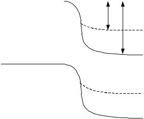
No current or voltage can be measured across the pn-junction unless light shines on it. In a complete circuit, the contact voltages of metallic leads will always be what is needed to cancel out the built-in voltage at the pn-junction. Otherwise, energy would not be conserved.
p
CB
n
ϕb – V0
ϕb = built-in
V0
VB
Fig. 6.25. The photoelectric effect for a pn-junction before and after illumination. The “before” are the solid lines and the “after” are the dashed lines. φb is the built-in potential and V0 is the potential produced by the cell
To understand physically the photovoltaic effect, consider Fig. 6.25. When light shines on the cell, electron–hole pairs are produced. Electrons produced in the p-region (within a diffusion length of the pn-junction) will tend to be swept over to the n-side and similarly for holes on the n-side. This reduces the voltage across the pn-junction from φb to φb − V0, say, and thus, produces a measurable forward voltage of V0. The maximum value of the output potential V0 from the solar cell is limited by the built-in potential φb.
V0 ≤ϕb ,
(6.251)
for if V0 = φb, then the built-in potential has been canceled and there is no potential left to separate electron–hole pairs.
In nondegenerate semiconductors suppose, before the p- and n- sides were “joined,” we let the Fermi levels be EF(p) and EF(n). When they are joined, equilibrium is established by electron–hole flow, which equalizes the Fermi energies. Thus, the built-in potential simply equals the original difference of Fermi energies
eϕb = EF (n) − EF ( p) .
(6.252)
348 6 Semiconductors
But, for the nondegenerate case
EF (n) − EF ( p) ≤ EC − EV = Eg .
(6.253)
Therefore,
eV0 ≤ Eg .
(6.254)
Smaller Eg means smaller photovoltages and, hence, less efficiency. By connecting several solar cells together in series, we can build a significant potential with arrays of pn-junctions. These connected cells power space satellites.
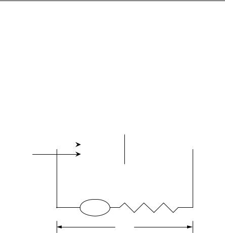
We give, now, an introduction to a more quantitative calculation of the behavior of a solar cell. Just as in our discussion of pn-junctions, we can find the total current by finding the minority current injected on each side. The only difference is that the external photons of light create electron–hole pairs. We assume the flux of photons is given by (see Fig. 6.26)
p
Light
n
x = –d
x = 0
x → large
I
V0
Fig. 6.26. A schematic of the solar cell
N (x) = N0 exp[−α(x + d)] ,
(6.255)
where α is the absorption coefficient, and it is a function of the photon wavelength. The rate at which electrons or holes are created per unit volume is
−
dN
=αN0 exp[−α(x + d)] .
(6.256)
dx
The equations for the minority carrier concentrations are just like those used for the pn-junction in (6.221) and (6.222), except now we must take into account the creation of electrons and holes by light from (6.256). We have
d2 (np − np
0
)
−
np − np
0
= −
αN
0 exp[−α(x + d)] , x < 0 , (6.257)
dx2
L2
Dn
n
6.3 Semiconductor Device Physics
349
and
d2 ( pn − pn
0
)
−
pn − pn
0
= −
αN
0 exp[−α(x + d)] , x > 0
. (6.258)
dx2
L2p
Dp
Both equations apply outside the depletion region when drift currents are negligible. The depletion region is so thin it is assumed to be treatable as being located in the plane x = 0.
By adding a particular solution of the inhomogeneous equation to a general solution of the homogeneous equation, we find
x
x
αN τ
n
np (x) − np0
+
0
exp[−α(x + d)] ,(6.259)
= a cosh
L
+ b sinh
L
1−α
2
2
n
n
L
n
and
x
αN0τ p
pn (x) − pn0 = d exp
−
+
1−α
2
2
exp[−α(x + d)] ,
(6.260)
Lp
Lp
where it has been assumed that pn approaches a finite value for large x. We now have three constants to evaluate (a), (b), and (d). We can use the following boundary conditions:
np (0)
eV
= exp
0
,
(6.261)
np0
kT
p
n
(0)
eV
= exp
0
,
(6.262)
pn
0
kT
and
D
d
(n
p
− n
p0
)
= S
p
[n
p
(−d ) − n
p0
].
(6.263)
n
dx
x=−d
This is a standard assumption that introduces a surface recombination velocity Sp. The total current as a function of V0 can be evaluated from
I = eA[J p (0) − Jn (0)] ,
(6.264)
where A is the cross-sectional area of the p-njunction. V0 is now the bias voltage across the pn-junction. The current can be evaluated from (with a negligibly thick depletion region)
JTotal = qDn
dnp
x<0 − qDp
dpn
x>0 .
(6.265)
dx
dx
x→0
x→0
For a modern update, see Martin Green, “Solar Cells” (Chap. 8 in Sze, [6.42]).
350 6 Semiconductors
6.3.10 Transistors (EE)
A power-amplifying structure made with pn-junctions is called a transistor. There are two main types of transistors: bipolar junction transistors (BJTs) and metaloxide semiconductor field effect transistors (MOSFETs). MOSFETs are unipolar (electrons or holes are the carriers) and are the most rapidly developing type partly because they are easier to manufacture. However, MOSFETs have large gate capacitors and are slower. The huge increase in the application of microelectronics is due to integrated circuits and planar manufacturing techniques (Sapoval and Hermann, [6.33, p 258]; Fraser, [6.14, Chap. 6]). MOSFETs may have smaller transistors and can thus be used for higher integration. A serious discussion of the technology of these devices would take us too far aside, but the student should certainly read about it. Three excellent references for this purpose are Streetman [6.40] and Sze [6.41, 6.42].
Although J. E. Lilienfied was issued a patent for a field effect device in 1935, no practical commercial device was developed at that time because of the poor understanding of surfaces and surface states. In 1947, Shockley, Bardeen, and Brattrain developed the point constant transistor and won a Nobel Prize for that work. Shockley invented the bipolar junction transistor in 1948. This work had been stimulated by earlier work of Schottky on rectification at a metalsemiconductor interface. A field effect transistor was developed in 1953, and the more modern MOS transistors were invented in the 1960s.
6.3.11 Charge-Coupled Devices (CCD) (EE)
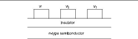
Charge-coupled devices (CCDs) were developed at Bell Labs in the 1970s and are now used extensively by astronomers for imaging purposes, and in digital cameras.
CCDs are based on ideas similar to those in metal-insulator-semiconductor structures that we just discussed. These devices are also called charge-transfer devices. The basic concept is shown in Fig. 6.27. Potential wells can be created under each electrode by applying the proper bias voltage.
V1,V2 ,V3 < 0 and V2 > V1 or V3 .
By making V2 more negative than V1, or V3, one can create a hole inversion layer under V2. Generally, the biasing is changed frequently enough that holes under V2 only come by transfer and not thermal excitation. For example, if we have holes under V2, simply by exchanging the voltages on V2 and V3 we can move the hole to under V3.
Since the presence or absence of charge is information in binary form, we have a way of steering or transferring information. CCDs have also been used to temporarily store an image. If we had large negative potentials at each Vi, then only those Vis, where light was strong enough to create electron–hole pairs, would have holes underneath them. The image is digitized and can be stored on a disk, which later can be used to view the image through a monitor.
Problems 351
Fig. 6.27. Schematic for a charge-coupled device
Problems
6.1For the nondegenerate case where E − μ >> kT, calculate the number of electrons per unit volume in the conduction band from the integral
n = ∫E∞c D(E) f (E)dE .
D(E) is the density of states, f(E) is the Fermi function. 6.2 Given the neutrality condition
Nc exp[−β(Ec − μ)] +
Nd
= Nd ,
1
+ a exp[β(Ed − μ)]
and the definition x = exp(βμ), solve the condition for x. Then solve for n in the region kT << Ec − Ed, where n = Ncexp[−β(Ec − μ)].
6.3Derive (6.45). Hint – look at Sect. 8.8 and Appendix 1 of Smith [6.38].
6.4Discuss in some detail the variation with temperature of the position of the Fermi energy in a fairly highly donor doped n-type semiconductor.
6.5Explain how the junction between two dissimilar metals can act as a rectifier.
6.6Discuss the mobility due to the lattice scattering of electrons in silicon or germanium. See, for example, Seitz [6.35].
6.7Discuss the scattering of charge carriers in a semiconductor by ionized donors or acceptors. See, for example, Conwell and Weisskopf [6.9].
6.8A sample of Si contains 10–4atomic per cent of phosphorous donors that are all singly ionized at room temperature. The electron mobility is 0.15 m2V–1s–1.
Calculate the extrinsic resistivity of the sample (for Si, atomic weight = 28, density = 2300 kg/m3).
6.9Derive (6.163) by use of the spatial constancy of the chemical potential.
7 Magnetism, Magnons, and Magnetic Resonance
The first chapter was devoted to the solid-state medium (i.e. its crystal structure and binding). The next two chapters concerned the two most important types of energy excitations in a solid (the electronic excitations and the phonons). Magnons are another important type of energy excitation and they occur in magnetically ordered solids. However, it is not possible to discuss magnons without laying some groundwork for them by discussing the more elementary parts of magnetic phenomena. Also, there are many magnetic properties that cannot be discussed by using the concept of magnons. In fact, the study of magnetism is probably the first solid-state property that was seriously studied, relating as it does to lodestone and compass needles.
Nearly all the magnetic effects in solids arise from electronic phenomena, and so it might be thought that we have already covered at least the fundamental principles of magnetism. However, we have not yet discussed in detail the electron’s spin degree of freedom, and it is this, as well as the orbital angular moment that together produce magnetic moments and thus are responsible for most magnetic effects in solids. When all is said and done, because of the richness of this subject, we will end up with a rather large chapter devoted to magnetism.
We will begin by briefly surveying some of the larger-scale phenomena associated with magnetism (diamagnetism, paramagnetism, ferromagnetism, and allied topics). These are of great technical importance. We will then show how to understand the origin of ordered magnetic structures from a quantum-mechanical viewpoint (in fact, strictly speaking this is the only way to understand it). This will lead to a discussion of the Heisenberg Hamiltonian, mean field theory, spin waves and magnons (the quanta of spin waves). We will also discuss the behavior of ordered magnetic systems near their critical temperature, which turns out also to be incredibly rich in ideas.
Following this we will discuss magnetic domains and related topics. This is of great practical importance.
Some of the simpler aspects of magnetic resonance will then be discussed as it not only has important applications, but magnetic resonance experiments provide direct measurements of the very small energy differences between magnetic sublevels in solids, and so they can be very sensitive probes into the inner details of magnetic solids.
We will end the chapter with some brief discussion of recent topics: the Kondo effect, spin glasses, magnetoelectronics, and solitons.
354 7 Magnetism, Magnons, and Magnetic Resonance
7.1 Types of Magnetism
7.1.1 Diamagnetism of the Core Electrons (B)
All matter shows diamagnetic effects, although these effects are often obscured by other stronger types of magnetism. In a solid in which the diamagnetic effect predominates, the solid has an induced magnetic moment that is in the opposite direction to an external applied magnetic field.
Since the diamagnetism of conduction electrons (Landau diamagnetism) has already been discussed (Sect. 3.2.2), this Section will concern itself only with the diamagnetism of the core electrons.
For an external magnetic field H in the z direction, the Hamiltonian (SI, e > 0) is given by
p2
e μ
0
H
∂
∂
e2 μ2 H 2
H =
+V (r) +
x
− y
+
0
(x2 + y2 ) .
2m
2mi
∂y
8m
∂x
For purely diamagnetic atoms with zero total angular momentum, the term involving first derivatives has zero matrix elements and so will be neglected. Thus, with a spherically symmetric potential V(r), the one-electron Hamiltonian is
H =
p2
+V (r) +
e2 μ02 H 2
(x2 + y 2 ) .
(7.1)
2m
8m
Let us evaluate the susceptibility of such a diamagnetic substance. It will be assumed that the eigenvalues of (7.1) (with H = 0) and the eigenkets |n are precisely known. Then by first-order perturbation theory, the energy change in state n due to the external magnetic field is
E′ =
e2μ02H 2
n | x2 + y2 | n .
(7.2)
8m
For simplicity, it will be assumed that |n is spherically symmetric. In this case
n | x2 + y2 | n =
2
n | r2
| n .
(7.3)
3
The induced magnetic moment μ can now be readily evaluated:
μ = −
∂E′
= −
e2μ0H
n | r2 | n .
(7.4)
∂(μ0H )
6m
If N is the number of atoms per unit volume, and Z is the number of core electrons, then the magnetization M is ZNμ, and the magnetic susceptibility χ is
χ =
∂M
= −
ZNe2μ0
n | r2 | n .
(7.5)
∂H
6m
7.1 Types of Magnetism
355
If we make an obvious reinterpretation of n|r2|n , then this result agrees with the classical result [7.39 p. 418]. The derivation of (7.5) assumes that the core electrons do not interact and that they are all in the same state |n . For core electrons on different atoms noninteraction would appear to be reasonable. However, it is not clear that this would lead to reasonable results for core electrons on the same atom. A generalization to core atoms in different states is fairly obvious.
A measurement of the diamagnetic susceptibility, when combined with theory (similar to the above), can sometimes provide a good test for any proposed forms for the core wave functions. However, if paramagnetic or other effects are present, they must first be subtracted out, and this procedure can lead to uncertainty in interpretation.
In summary, we can make the following statements about diamagnetism:
1.Every solid has diamagnetism although it may be masked by other magnetic effects.
2.The diamagnetic susceptibility (which is negative) is temperature independent (assuming we can regard n|r2|n as temperature independent).
7.1.2 Paramagnetism of Valence Electrons (B)
This Section is begun by making several comments about paramagnetism:
1.One form of paramagnetism has already been studied. This is the Pauli paramagnetism of the free electrons (Sect. 3.2.2).
2.When discussing paramagnetic effects, in general both the orbital and intrinsic spin properties of the electrons must be considered.
3.A paramagnetic substance has an induced magnetic moment in the same direction as the applied magnetic field.
4.When paramagnetic effects are present, they generally are much larger than the diamagnetic effects.
5.At high enough temperatures, all substances appear to behave in either a paramagnetic fashion or a diamagnetic fashion (even ferromagnetic solids, as we will discuss, become paramagnetic above a certain temperature).
6.The calculation of the paramagnetic susceptibility is a statistical problem, but the general reason for paramagnetism is unpaired electrons in unfilled shells of electrons.
7.The study of paramagnetism provides a natural first step for understanding ferromagnetism.
The calculation of a paramagnetic susceptibility will only be outlined. The perturbing part of the Hamiltonian is of the form [94], e > 0,
H ′ =
eμ0 H
(L + 2S) ,
(7.6)
2m
356 7 Magnetism, Magnons, and Magnetic Resonance
where L is the total orbital angular momentum operator, and S is the total spin operator. Using a canonical ensemble, we find the magnetization of a sample to be given by
F − H ′
,
(7.7)
M = NTr
μexp
kT
where N is the number of atoms per unit volume, μ is the magnetic moment operator proportional to (L + 2S), and F is the Helmholtz free energy.
Once (7.7) has been computed, the magnetic susceptibility is easily evaluated by means of
χ ≡
∂ M .
(7.8)
∂H
Equations (7.7) and (7.8) are always appropriate for evaluating χ, but the form of the Hamiltonian is modified if one wants to include complicated interaction effects.
At lower temperatures we expect that interactions such as crystal-field effects will become important. Properly including these effects for a specific problem is usually a research problem. The effects of crystal fields will be discussed later in the chapter.
Let us consider a particularly simple case of paramagnetism. This is the case of a particle with spin S (and no other angular momentum). For a magnetic field in the z-direction we can write the Hamiltonian as (charge on electron is e > 0)
H ′ =
eμ0H
2Sz .
(7.9)
2m
Let us define gμB in such a way that the eigenvalues of (7.9) are
E = gμBμ0HM S ,
(7.10)
where μB = e /2m is the Bohr magneton, and g is sometimes called simply the g- factor. The use of a g-factor allows our formalism to include orbital effects if necessary. In (7.10) g = 2 (spin only).
If N is the number of particles per unit volume, then the average magnetization can be written as1
∑MS
S =−S M S gμB exp(M S gμB μ0 H / kT )
(7.11)
M = N
∑MS
.
S =−S exp(M S gμB μ0 H / kT )
1 Note that μB has absorbed the so MS and S are either integers or half-integers. Also note (7.11) is invariant to a change of the dummy summation variable from MS to −MS.