

Patterson, Bailey - Solid State Physics Introduction to theory
.pdf6.1 Electron Motion |
317 |
|
|
Power Absorption in Cyclotron Resonance (A)
Here we show how a resonant frequency gives a maximum in the power absorption versus field, as for example in Fig. 6.7. We will calculate the power absorption by evaluating the complex conductivity. We use (6.86) with v being the drift velocity of the appropriate charge carrier with effective mass m* and charge q = −e. This equation neglects interactions between charge carriers in semiconductors since the carrier density is low and they can stay out of each others way. In (6.86), τ is the relaxation time and the 1/τ terms take care of the damping effect of collisions. As usual the carriers will be assumed to be quasifree (free electrons with an effective mass to include lattice effects) and we assume that the wave packets describing the carriers spread little so the carriers can be treated classically.
Let the B field be a static field along the z-axis and let E = Exeiωti be the planepolarized electric field. Solutions of the form
v(t) = veiωt , |
(6.134) |
will be sought. Then (6.86) may be written in component form as
m (iω)vx = qEx + qvy B − |
m |
vx , |
(6.135) |
|||
|
||||||
|
|
|
τ |
|
|
|
m (iω)vy = −qvx B − |
m |
vy . |
(6.136) |
|||
τ |
||||||
|
|
|
|
|||
If we assume the carriers are electrons then j = nevx(–e) = σEx so the complex conductivity is
σ = − |
enevx |
, |
(6.137) |
|
|||
|
Ex |
|
|
where ne is the concentration of electrons. By solving (6.136) and (6.137) we find
σ =σ0 |
[1+ (ωc2 −ω2 )τ 2 ] + 2ω2τ 2 |
+ iσ0 |
ωτ[1+ (ωc2 −ω2 )τ 2 − 2] |
, (6.138) |
||||||
[1 |
+ (ωc2 |
−ω2 )τ 2 ]2 |
+ 4ω2τ 2 |
[1+ (ωc2 |
−ω2 )τ 2 ]2 |
+ 4ω2τ 2 |
||||
|
|
|
||||||||
where σ0 = nee2τ/m* is the dc conductivity and ωc = eB/m*.
The rate at which energy is lost (per unit volume) due to Joule heating is j·E = jxEx. But
Re( jx ) = Re(σEx )
= Re[(σr + iσi )(Ex cosωt + iEx sinωt)] (6.139) =σr Ex cosωt −σi Ex sinωt .
So
Re( jx ) Re(Ec ) = Ex2 (σr cos2 ωt −σi cosωt sinωt) . |
(6.140) |

|
|
|
|
|
|
|
|
|
|
|
|
|
|
|
|
|
|
|
|
|
|
|
|
|
|
|
|
|
6.2 Examples of Semiconductors |
319 |
||||||||||
|
|
|
|
|
|
|
|
|
|
|
|
|
|
|
|
|
|
|
|
|
|
|
|
|
|
|
|
|
|
|
|
|
|
|
|
|
|
|
|
|
|
|
|
|
|
|
|
|
|
|
|
|
|
|
|
|
|
|
|
|
|
|
|
|
|
|
|
|
|
|
|
|
|
|
|
|
|
|
|
|
|
|
|
|
|
|
|
|
|
|
|
|
|
|
|
|
|
|
|
|
|
|
|
|
|
|
|
|
|
|
|
|
|
|
|
|
|
|
|
|
|
|
|
|
|
|
|
|
|
|
|
|
|
|
|
|
|
|
|
|
|
|
|
|
|
|
|
|
|
|
|
|
|
|
|
|
|
|
|
|
|
|
|
|
|
|
|
|
|
|
|
|
|
|
|
|
|
|
|
|
|
|
|
|
|
|
|
|
|
|
|
|
|
|
|
|
|
|
|
|
|
|
|
|
|
|
|
|
|
|
|
|
|
|
|
|
|
|
|
|
|
|
|
|
|
|
|
|
|
|
|
|
|
|
|
|
|
|
|
|
|
|
|
|
|
|
|
|
|
|
|
|
|
|
|
|
|
|
|
|
|
|
|
|
|
|
|
|
|
|
|
|
|
|
|
|
|
|
|
|
|
|
|
|
|
|
|
|
|
|
|
|
|
|
|
|
|
|
|
|
|
|
|
|
|
|
|
|
|
|
|
|
|
|
|
|
|
|
|
|
|
|
|
|
|
|
|
|
|
|
|
|
|
|
|
|
|
|
|
|
|
|
|
|
|
|
|
|
|
|
|
|
|
|
|
|
|
|
|
|
|
|
|
|
|
|
|
|
|
|
|
|
|
|
|
|
|
|
|
|
|
|
|
|
|
|
|
|
|
|
|
|
|
|
|
|
|
|
|
|
|
|
|
|
|
|
|
|
|
|
|
|
|
|
|
|
|
|
|
|
|
|
|
|
|
|
|
|
|
|
|
|
|
|
|
|
|
|
|
|
|
|
|
|
|
|
|
|
|
|
|
|
|
|
|
|
|
|
|
|
|
|
|
|
|
|
|
|
|
|
|
|
|
|
|
|
|
|
|
|
|
|
|
|
|
|
|
|
|
|
|
|
|
|
|
|
|
|
|
|
|
|
|
|
|
|
|
|
|
|
|
|
|
|
|
|
|
|
|
|
|
|
|
|
|
|
|
|
|
|
|
|
|
|
|
|
|
|
|
|
|
|
|
|
|
|
|
|
|
|
|
|
|
|
|
|
|
|
|
|
|
|
|
|
|
|
|
|
|
|
|
|
|
|
|
|
|
|
|
|
|
|
|
|
|
|
|
|
|
|
|
|
|
|
|
|
|
|
|
|
|
|
|
|
|
|
|
|
|
|
|
|
|
|
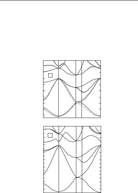
Fig. 6.9. Theoretical pseudopotential electronic valence densities of states compared with experiment for Si and Ge. Adaptation reprinted with permission from Cheliokowsky JR and Cohen ML, Phys Rev B 14, 556 (1976). Copyright 1976 by the American Physical Society
6.2 Examples of Semiconductors
6.2.1Models of Band Structure for Si, Ge and II-VI and III-V Materials (A)
First let us give some band structure and density of states for Si and Ge. See Fig. 6.8 and Fig. 6.9. The figures illustrate two points. First, that model calculation tools using the pseudopotential (see “The Pseudopotential Method” under Sect. 3.2.3) have been able to realistically model actual semiconductors. Second, that the models we often use (such as the simplified pseudopotential) are oversimplified but still useful


|
6.2 Examples of Semiconductors |
323 |
|
|
|
|
|
|
|
|
|
|
|
|
|
|
|
|
|
|
|
|
|
|
|
|
|
|
|
|
|
|
|
|
|
|
|
|
|
|
|
|
|
|
|
|
|
|
|
|
|
|
|
|
|
|
|
|
|
|
|
|
|
|
|
|
|
|
|
|
|
|
|
|
|
|
|
|
|
|
|
|
|
|
|
|
|
|
|
|
|
|
|
|
|
|
|
|
|
|
|
|
|
|
|
|
|
|
|
|
|
|
|
|
|
|
|
|
|
|
|
|
|
|
|
Fig. 6.11. Zincblende lattice structure. The shaded sites are occupied by one type of ion, the unshaded by another type
[001] |
kz |
|
|
|
|
||
|
X |
|
|
|
|
L |
|
|
Γ |
|
[010] |
|
|
|
|
|
|
X |
ky |
[100] |
X |
|
|
kx |
|
L |
|
|
|
[111] |
|
Fig. 6.12. First Brillouin zone for zincblende lattice structure. Certain symmetry points are denoted with the usual notation

6.3 Semiconductor Device Physics |
325 |
|
|
Sect. 12.4) with AlGaN and thus HFETs (heterostructure field effect transistors) have been made. Transistors of both high power and high frequency have been produced with GaN. It also has good mechanical properties, and can work at higher temperature as well as having good thermal conductivity and a high breakdown field. GaN has become very important for recent advances in solid-state lighting. Studies of dopants, impurities, and defects are important for improving the light-emitting efficiency.
GaN is famous for its use in making blue lasers. See Nakamura et al [6.26], Pankove and Moustaka (eds) [6.28], and Willardson and Weber [6.43].
6.3 Semiconductor Device Physics
This Section will give only some of the flavor and some of the approximate device equations relevant to semiconductor applications. The book by Dalven [6.10] is an excellent introduction to this subject. So is the book by Fraser [6.14]. The most complete book is by Sze [6.41]. In recent years layered structures with quantum wells and other new effects are being used for semiconductor devices. See Chap. 12 and references [6.1, 6.19]
6.3.1 Crystal Growth of Semiconductors (EE, MET, MS)
The engineering of semiconductors has been as important as the science. By engineering we mean growth, purification, and controlled doping. In Chap. 12 we go a little further and talk of the band engineering of semiconductors. Here we wish to consider growth and related matters. For further details, see Streetman [6.40, p12ff]. Without the ability to grow extremely pure single crystal Si, the semiconductor industry as we know it would not have arisen. With relatively few electrons and holes, semiconductors are just too sensitive to impurities.
To obtain the desired pure crystal semiconductor, elemental Si, for example, is chemically deposited from compounds. Ingots are then poured that become polycrystalline on cooling.
Single crystals can be grown by starting with a seed crystal at one end and passing a molten zone down a “boat” containing the seed crystal (the molten zone technique), see Fig. 6.14.
Since the boat can introduce stresses (as well as impurities) an alternative method is to grow the crystal from the melt by pulling a rotating seed from it (the
Czochralski technique), see Fig. 6.14b.