6.1 Electron Motion
6.1.1 Calculation of Electron and Hole Concentration (B)
Here we give the standard calculation of carrier concentration based on (a) excitation of electrons from the valence to the conduction band leaving holes in the valence band, (b) the presence of impurity donors and acceptors (of electrons) and
(c) charge neutrality. This discussion is important for electrical conductivity among other properties.
We start with a simple picture assuming a parabolic band structure of semiconductors involving conduction and valence bands as shown in Fig. 6.1. We will later find our results can be generalized using a suitable effective mass (Sect.6.1.6). Here when we talk about donor and acceptor impurities we are talking about shallow defects only (where the energy levels of the donors are just below the conduction band minimum and of acceptors just above the valence-band maximum). Shallow defects are further discussed in Sect. 11.2. Deep defects are discussed and compared to shallow defects in Sect. 11.3 and Table 11.1. We limit ourselves in this chapter to impurities that are sufficiently dilute that they form localized and discrete levels. Impurity bands can form where 4πa3n/3 1 where a is the lattice constant and n is the volume density of impurity atoms of a given type.
The charge-carrier population of the levels is governed by the Fermi function f. The Fermi function evaluated at the Fermi energy E = μ is 1/2. We have assumed μ is near the middle of the band. The Fermi function is given by
f (E) = |
|
1 |
|
|
|
. |
(6.1) |
|
E − |
μ |
|
|
|
|
|
|
exp |
|
|
|
+1 |
|
|
kT |
|
|
|
|
|
|
|
|
|
In Fig. 6.1 EC is the energy of the bottom of the conduction band. EV is the energy of the top of the valence band. ED is the donor state energy (energy with one electron and in which case the donor is assumed to be neutral). EA is the acceptor state energy (which when it has two electrons and no holes is singly charged). For more on this model see Table 6.3 and Table 6.4. Some typical donor and acceptor energies for column IV semiconductors are 44 and 39 meV for P and Sb in Si, 46 and 160 meV for B and In in Si.1
We now evaluate expressions for the electron concentration in the conduction band and the hole concentration in the valence band. We assume the nondegenerate case when E in the conduction band implies (E − μ) >> kT, so
|
|
E − |
μ |
|
f (E) exp |
− |
|
|
. |
(6.2) |
kT |
|
|
|
|
|
|
|
E |
CB |
E |
|
|
|
EC |
|
|
|
ED |
|
|
|
μ |
|
Fermi Energy |
|
|
|
|
EA |
|
|
|
EV |
|
D(E) |
f(E) |
|
|
(Density of |
(Fermi |
|
|
States) |
Function) |
|
|
VB |
|
Fig. 6.1. Energy gaps, Fermi function, and defect levels (sketch). Direction of increase of D(E), f(E)is indicated by arrows
We further assume a parabolic band, so
|
2k 2 |
|
E = |
|
+ EC , |
(6.3) |
2m |
|
e |
|
where me* is a constant. For such a case we have shown (in Chap. 3) the density of states is given by
|
1 |
|
2m 3 / 2 |
|
|
D(E) = |
|
|
e |
E − EC . |
(6.4) |
2π |
2 |
2 |
|
|
|
|
|
The number of electrons per unit volume in the conduction band is given by:
n = ∫∞ D(E) f (E)dE . |
(6.5) |
EC |
|
Evaluating the integral, we find
m kT 3 / 2 |
μ − E |
C |
|
|
|
e |
|
|
exp |
|
. |
|
n = 2 |
2π |
2 |
|
kT |
|
(6.6) |
|
|
|
|
|
|
|
For holes, we assume, following (6.3),
|
E = EV − |
2k 2 |
, |
(6.7) |
|
2mh |
|
|
|
|
which yields the density of states
Dh (E) =
The number of holes per state is
fh =1−
1 |
|
|
2m 3 / 2 |
|
− E . |
|
2 |
|
|
n |
E |
V |
2π |
|
2 |
|
|
|
|
|
|
|
|
|
|
|
|
|
f (E) |
= |
|
|
1 |
|
|
. |
|
|
μ − E |
|
|
|
|
|
|
|
|
|
|
|
|
|
exp |
|
|
+1 |
|
|
|
kT |
|
|
|
|
|
|
|
|
|
Again, we make a nondegeneracy assumption and assume (μ − E) >> kT for E in the valence band, so
|
|
|
|
E − μ |
|
|
|
|
|
fh exp |
|
|
|
. |
|
|
(6.10) |
|
|
kT |
|
|
|
|
|
|
|
|
|
|
|
|
|
The number of holes/volume in the valence band is then given by |
|
p = ∫EV |
Dh (E) fh (E)dE , |
|
(6.11) |
|
−∞ |
|
|
|
|
|
|
|
|
|
from which we find |
|
|
|
|
|
|
|
|
|
|
|
m kT 3/ 2 |
|
E |
V |
− μ |
|
|
h |
|
|
exp |
|
|
|
. |
|
p = 2 |
2π |
2 |
|
|
|
kT |
(6.12) |
|
|
|
|
|
|
|
|
Since the density of states in the valence and conduction bands is essentially unmodified by the presence or absence of donors and acceptors, the equations for n and p are valid with or without donors or acceptors. (Donors or acceptors, as we will see, modify the value of the chemical potential, μ.) Multiplying n and p, we find
|
|
|
np = n2 |
, |
|
|
|
i |
|
where |
|
|
|
|
|
kT |
|
3/ 2 |
|
ni = 2 |
|
|
(me mh )3 / 4 |
|
2 |
2π |
|
|
where Eg = EC − EV is the bandgap and ni is the intrinsic (without donors or acceptors) electron concentration. Equation (6.13) is sometimes called the Law of Mass Action and is generally true since it is independent of μ.
We now turn to the question of calculating the number of electrons on donors and holes on acceptors. We use the basic theorem for a grand canonical ensemble (see, e.g., Ashcroft and Mermin, [6.2, p 581])
|
n = |
∑ j N jexp[−β(E j − μN j )] |
, |
(6.15) |
|
∑ j exp[−β(E j − μN j )] |
|
|
|
|
where β = 1/kT and n = mean number of electrons in a system with states j, with energy Ej, and number of electrons Nj.
|
|
|
6.1 Electron Motion 299 |
|
|
|
|
Table 6.3. Model for energy and degeneracy of donors |
|
|
|
|
|
|
Number of electrons |
Energy |
Degeneracy of state |
|
|
|
|
|
|
Nj = 0 |
0 |
1 |
|
|
Nj = 1 |
Ed |
2 |
|
|
Nj = 2 |
→ ∞ |
neglect as too improbable |
|
|
|
|
|
We are considering a model of a donor level that is doubly degenerate (in a single-particle model). Note that it is possible to have other models for donors and acceptors. There are basically three cases to look at, as shown in Table 6.3. Noting that when we sum over states, we must include the degeneracy factors. For the mean number of electrons on a state j as defined in Table 6.3
n = |
(1)(2) exp[−β(Ed − μ)] |
, |
|
(6.16) |
1+ 2 exp[−β(Ed − μ)] |
|
|
or |
|
|
|
|
|
|
|
|
|
|
n = |
|
|
1 |
|
= |
|
nd |
, |
(6.17) |
1 |
|
|
|
|
|
|
exp[−β(Ed − μ)] +1 |
|
|
Nd |
|
|
2 |
|
|
|
|
|
|
|
|
|
|
|
|
|
where nd is the number of electrons/volume on donor atoms and Nd is the number of donor atoms/volume. For the acceptor case, our model is given by Table 6.4.
Table 6.4. Model for energy and degeneracy of acceptors
Number of electrons |
Number of holes |
Energy |
Degeneracy |
|
|
|
|
0 |
2 |
very large |
neglect |
1 |
1 |
0 |
2 |
2 |
0 |
EA |
1 |
The number of electrons per acceptor level of the type defined in Table 6.4 is
n = |
(1)(2) exp[−β(−μ)] + 2(1) exp[−β(Ea − 2μ)] |
, |
(6.18) |
|
2 exp[βμ] + exp[−β(Ea − 2μ)] |
|
|
which can be written |
|
|
|
|
|
|
|
|
n = |
|
exp[β(μ − Ea )] +1 |
|
|
|
|
|
|
. |
|
(6.19) |
|
|
1 |
exp[β(μ − Ea )] +1 |
|
|
|
|
|
|
2 |
|
|
|
|

Now, the average number of electrons plus the average number of holes associated with the acceptor level is 2. So, n + p = 2. We thus find
p |
= |
pa = |
|
1 |
|
, |
(6.20) |
|
1 |
|
|
|
|
Na |
exp[β(μ − Ea )] +1 |
|
|
|
|
2 |
|
|
|
|
|
|
|
|
|
|
where pa is the number of holes/volume on acceptor atoms. Na is the number of acceptor atoms/volume.
So far, we have four equations for the five unknowns n, p, nd, pa, and μ. A fifth equation, determining μ can be found from the condition of electrical neutrality. Note:
N |
d |
− n ≡ number of ionized and, hence, positive donors ≡ N + , |
|
d |
d |
|
|
Na − pa ≡ number of negative acceptors = N a− . |
|
Charge neutrality then says, |
|
|
|
p + Nd+ = n + N a− , |
(6.21) |
or |
|
|
|
|
|
n + Na + nd = p + Nd + pa . |
(6.22) |
We start by discussing an example of the exhaustion region where all the donors are ionized. We assume Na = 0, so also pa = 0. We assume kT << Eg, so also p = 0. Thus, the electrical neutrality condition reduces to
We also assume a temperature that is high enough that all donors are ionized. This requires kT >> Ec − Ed. This basically means that the probability that states in the donor are occupied is the same as the probability that states in the conduction band are occupied. But, there are many more states in the conduction band compared to donor states, so there are many more electrons in the conduction band. Therefore nd << Nd or n Nd. This is called the exhaustion region of donors.
As a second example, we consider the same situation, but now the temperature is not high enough that all donors are ionized. Using
|
nd = |
|
|
|
Nd |
|
|
|
. |
(6.24) |
|
1 |
+ a exp[β(Ed − μ)] |
|
|
|
|
|
In our model a = 1/2, but different models could yield different a. Also |
|
|
n = Nc exp[−β(Ec − μ)] , |
|
(6.25) |
|
where |
|
|
|
|
|
|
|
|
|
|
|
|
|
m kT 3/ 2 |
|
|
|
|
|
|
|
|
|
e |
|
|
|
|
|
|
Nc = 2 |
|
|
. |
|
|
(6.26) |
|
|
|
|
2π 2 |
|
|
|
|
E |
Ec |
Ed |
μ |
(intrinsic) |
μi |
T |
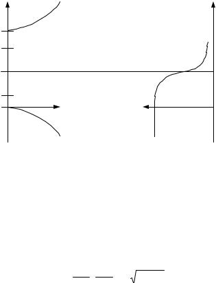
Fig. 6.2. Sketch of variation of Fermi energy or chemical potential μ, with temperature for Na = 0 and Nd > 0
Fig. 6.3. Energy gaps, Fermi function, and defect levels (sketch)
The neutrality condition then gives
|
Nc exp[−β(Ec − μ)] + |
|
|
Nd |
= Nd . |
(6.27) |
|
1 |
+ a exp[β(Ed − μ)] |
|
|
|
|

Defining x = eβμ, the above gives a quadratic equation for x. Finding the physically realistic solution for low temperatures, kT << (Ec − Ed), we find x and, hence,
n = a Nc Nd exp[−β(Ec − Ed ) / 2] . |
(6.28) |
This result is valid only in the case that acceptors can be neglected, but in actual impure semiconductors this is not true in the low-temperature limit. More detailed considerations give the variation of Fermi energy with temperature for Na = 0 and Nd > 0 as sketched in Fig. 6.2. For the variation of the majority carrier density for Nd > Na ≠ 0, we find something like Fig. 6.3.
6.1.2 Equation of Motion of Electrons in Energy Bands (B)
We start by discussing the dynamics of wave packets describing electrons [6.33, p23]. We need to do this in order to discuss properties of semiconductors such as the Hall effect, electrical conductivity, cyclotron resonance, and others. In order to think of the motion of charge, we need to think of the charge being transported by the wave packets.2 The three-dimensional result using free-electron wave packets can be written as
This result, as we now discuss, is appropriate even if the wave packets are built out of Bloch waves.
Let a Bloch state be represented by
ψnk = unk (r)eik r , |
(6.30) |
where n is the band index and unk(r) is periodic in the space lattice. With the Hamiltonian
|
1 |
|
|
2 |
|
H = |
|
|
|
|
+V (r) , |
(6.31) |
|
|
|
2m i |
|
|
|
where V(r) is periodic, |
|
|
|
|
|
|
Hψnk = Enkψnk , |
(6.32) |
and we can show |
|
|
|
|
|
|
H k unk = Enkunk , |
(6.33) |
2The standard derivation using wave packets is given by, e.g., Merzbacher [6.24]. In Merzbacher’s derivation, the peak of the wave packet moves with the group velocity.
where
|
2 |
1 |
|
2 |
H k = |
|
|
+ k |
+ V (r) . |
|
|
2m i |
|
|
Note
H k +qunk +q = Enk +qunk +q ,
and to first order in q:
|
|
|
2 |
|
|
|
1 |
|
|
|
H k +q = H k + |
|
|
q |
|
|
+ k . |
|
m |
|
|
|
|
|
|
i |
|
|
|
To first order |
|
|
|
|
|
|
|
|
|
|
En (k + q) = En (k) + q k Enk . |
|
Also by first-order perturbation theory |
|
|
|
|
|
|
|
|
|
|
|
|
|
|
2 |
|
1 |
|
|
En (k + q) = En (k) + ∫ unk |
|
|
|
|
q |
|
+ k unkdV . |
|
|
m |
|
|
|
|
|
|
|
|
i |
|
|
From this we conclude |
|
|
|
|
|
|
|
|
|
|
k Enk = ∫ unk |
|
2 |
1 |
|
|
|
|
|
|
|
|
+ k unkdV |
|
|
m i |
|
|
|
|
|
= ∫ψnk |
mi |
ψnkdV |
|
= ψnk |
|
p |
ψnk . |
|
|
|
|
m |
|
|
|
|
|
|
Thus if we define
v = ψnk mp ψnk ,
(6.34)
(6.35)
(6.36)
(6.37)
(6.38)
(6.39)
(6.40)
then v equals the average velocity of the electron in the Bloch state nk. So we find
v = 1 k Enk .
Note that v is a constant velocity (for a given k). We interpret this as meaning that a Bloch electron in a periodic crystal is not scattered.
Note also that we should use a packet of Bloch waves to describe the motion of electrons. Thus we should average this result over a set of states peaked at k. It can also be shown following standard arguments (Smith [6.38], Sect. 4.6) that (6.29) is the appropriate velocity of such a packet of waves.

We now apply external fields and ask what is the effect of these external fields on the electrons. In particular, what is the effect on the electrons if they are already in a periodic potential? If an external force Fext acts on an electron during a time interval δt, it produces a change in energy given by
δE = Fextδx = Fvgδt . |
(6.41) |
Substituting for vg, |
|
|
|
|
|
|
δE = |
F |
|
1 |
δE δt . |
(6.42) |
|
|
|
ext |
|
δk |
|
Canceling out δE, we find |
|
|
|
|
|
|
F |
|
= |
|
δk |
. |
(6.43) |
|
|
|
ext |
|
|
δt |
|
|
|
|
|
|
The three-dimensional result may formally be obtained by analogy to the above:
ext dt
In general, F is the external force, so if E and B are electric and magnetic fields, then
|
dk |
= −e(E + v × B) |
(6.45) |
|
dt |
|
|
|
for an electron with charge −e. See Problem 6.3 for a more detailed derivation. This result is often called the acceleration theorem in k-space.
We next introduce the concept of effective mass. In one dimension, by taking the time derivative of the group velocity we have
dv = 1 d2E dk = |
1 |
|
d2E F . |
(6.46) |
|
|
|
|
dt |
|
dk 2 |
dt |
|
2 |
|
dk 2 |
ext |
|
|
|
|
|
|
Defining the effective mass so |
|
|
|
|
|
|
|
|
|
|
|
|
|
|
|
|
|
|
F |
= m |
dv |
, |
|
|
|
(6.47) |
|
|
|
|
|
|
|
|
|
ext |
|
|
|
|
dt |
|
|
|
|
|
|
|
|
|
|
|
|
|
|
|
|
|
|
|
|
we have |
|
|
|
|
|
|
|
|
|
|
|
|
|
|
|
|
|
m = |
|
|
2 |
|
|
|
. |
|
|
(6.48) |
|
|
|
|
|
|
|
|
|
|
|
|
|
|
d2E / dk 2 |
|
|
|
|
|
|
|
|
|
|
In three dimensions: |
|
|
|
|
|
|
|
|
|
|
|
|
|
|
|
|
1 |
|
1 |
|
|
∂ 2E |
|
|
|
|
|
|
|
= |
|
|
|
|
|
|
. |
(6.49) |
|
|
2 |
∂k |
|
∂k |
β |
m |
|
|
|
|
|
|
α |
|
|
|
|
|
|
|
αβ |
|
|
|
|
|
|
|
|
|
|
|
|
|
|
|
|
|
6.1 Electron Motion |
305 |
|
|
|
Notice in the free-electron case when E =ħ2k2/2m, |
|
|
1 |
|
δαβ |
|
|
|
|
|
= |
|
. |
(6.50) |
|
|
m αβ |
|
m |
|
|
6.1.3 Concept of Hole Conduction (B)
The totality of the electrons in a band determines the conduction properties of that band. But, when a band is nearly full it is usually easier to consider holes that represent the absent electrons. There will be far fewer holes than electrons and this in itself is a huge simplification.
It is fairly easy to see why an absent electron in the valence band acts as a positive electron. See also Kittel [6.17, p206ff]. Let f label filled electron states, and g label the states that will later be emptied. For a full band in a crystal, with volume V, for conduction in the x direction,
|
|
|
|
|
|
|
|
|
|
|
|
|
|
|
jx = − |
e |
∑ |
f |
vxf − |
e |
∑ |
g |
vxg |
= 0 , |
(6.51) |
|
|
|
|
V |
|
V |
|
|
|
|
|
|
so that |
|
|
|
|
|
|
|
|
|
|
|
|
∑ f vxf |
= −∑g vxg . |
|
(6.52) |
If g states of the band are now emptied, then the current is given by |
|
jx = − |
e |
∑ f vxf = |
|
e |
∑g vxg . |
(6.53) |
|
|
|
|
V |
|
|
|
|
V |
|
|
|
|
Notice this argument means that the current in a partially empty band can be considered as due to holes of charge +e, which move with the velocities of the states that are missing electrons. In other words, qh = +e and vh = ve.
Now, let us talk about the energy of the holes. Consider a full band with one missing electron. Let the wave vector of the missing electron be ke and the corresponding energy Ee(ke):
Esolid, full band = Esolid, one missing electron + Ee (ke ) . |
(6.54) |
Since the hole energy is the energy it takes to remove the electron, we have
Hole energy = Esolid, one missing electron − Esolid, full band = −Ee (ke ) (6.55)
by using the above. Now in a full band the sum of the k is zero. Since we identify the hole wave vector as the totality of the filled electronic states
ke + ∑ ′k = 0 , |
(6.56) |
kh = ∑ ′k = −ke , |
(6.57) |