|
pull |
|
|
seed |
|
seed molten zone |
turn |
|
|
|
boat |
molten crystal |
container |
polycrystal |
|
|
(a) |
(b) |
|
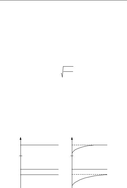
Fig. 6.14. (a) The molten zone technique for crystal growth and (b) the Czochralski Technique for crystal growth
Purification can be achieved by passing a molten zone through the crystal. This is called zone refining. The impurities tend to concentrate in the molten zone, and more than one pass is often useful. A variation is the floating zone technique where the crystal is held vertically and no walls are used.
There are other crystal growth techniques. Liquid phase epitaxy and vapor phase epitaxy, where crystals are grown below their melting point, are discussed by Streetman (see reference above). We discuss molecular beam epitaxy, important in molecular engineering, in Chap. 12.
In order to make a semiconductor device, initial purity and controlled introduction of impurities is necessary. Diffusion at high temperatures is often used to dope or introduce impurities. An alternative process is ion implantation that can be done at low temperature, producing well-defined doping layers. However, lattice damage may result, see Streetman [6.40, p128ff], but this can often be removed by annealing.
6.3.2 Gunn Effect (EE)
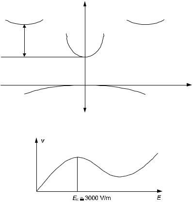
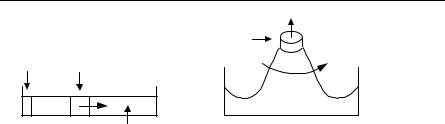
The Gunn effect is the generation of microwave oscillations in a semiconductor like GaAs or InP (or other III-V materials) due to a high (of order several thousand V/cm) electric field. The effect arises due to the energy band structure sketched in Fig. 6.15.
Since m* (d2E/dk2)−1, we see m2* > m1*, or m2 is heavy compared to m1. The applied electric field can supply energy to the electrons and raise them from the m1* (where they would tend to be) part of the band to the m2* part. With their gain in mass, it is possible for the electrons to experience a drop in drift velocity (mobility = v/E 1/m*).
If we make a plot of drift velocity versus electric field, we get something like Fig. 6.16. The differential conductivity is
6.3 Semiconductor Device Physics |
327 |
|
|
|
|
E |
|
|
m2* ~ 0.6m |
|
|
(reduced |
|
|
mobility) |
|
~ 0.36eV |
m1* ~ 0.07m |
|
μ ~ 0.5 |
|
|
|
|
k |
|
|
–E |
Fig. 6.15. Schematic of energy band structure for GaAs used for Gunn effect
Fig. 6.16. Schematic of electron drift velocity vs. electric field in GaAs
where J is the electrical current density that for electrons we can write as J = nev, where v = |v|, e > 0. Thus,
|
σd = ne |
dv |
< 0 , |
(6.152) |
|
dE |
|
|
|
|
when E > Ec and is not too large. This is the region of bulk negative conductivity (BNC), and it is unstable and leads to the Gunn effect. The generation of Gunn microwave oscillations may be summarized by the following three statements:
1.Because the electrons gain energy from the electric field, they transfer to a region of E(k) space where they have higher masses. There, they slow down, “pile up”, and form space-charge domains that move with an overall drift velocity v.
2.We assume the length of the sample is l. A current pulse is delivered for every domain transit.

3.Because of reduction of the electric field external to the domain, once a domain is formed, another is not formed until the first domain drifts across.
The frequency of the oscillation is approximately
|
f = |
v |
≈ |
107 m/s |
≈10GHz . |
(6.153) |
|
l |
10−3 m |
|
|
|
|
|
The instability with respect to charge domain-foundation can be simply argued. In one dimension from the continuity equation and Gauss’ law, we have
|
|
|
|
|
|
∂J |
+ |
∂ρ |
|
= 0 , |
|
|
|
|
|
(6.154) |
|
|
|
|
|
|
|
|
|
|
∂t |
|
|
|
|
|
|
|
|
|
|
∂x |
|
|
|
|
|
|
|
|
|
|
|
|
|
|
|
|
|
|
|
∂E |
= |
ρ |
|
, |
|
|
|
|
|
|
(6.155) |
|
|
|
|
|
|
|
|
∂x |
ε |
|
|
|
|
|
|
|
|
|
|
|
|
|
|
|
|
|
|
|
|
|
|
|
|
|
|
∂J |
|
= |
∂J |
|
|
∂E |
= σd |
|
ρ |
. |
(6.156) |
|
∂x |
|
|
|
∂x |
|
|
|
|
|
|
∂E |
|
|
|
|
|
|
|
ε |
|
So, |
|
|
|
|
|
|
|
|
|
|
|
|
|
|
|
|
|
|
|
|
|
|
|
|
|
∂ρ |
|
= − |
∂J |
= −σd |
|
ρ |
, |
(6.157) |
|
|
∂τ |
|
|
|
|
|
|
|
|
|
|
|
|
∂x |
|
|
|
|
|
ε |
|
or |
|
|
|
|
|
|
|
|
|
|
|
|
|
|
|
|
|
|
|
|
|
|
|
|
|
|
|
|
|
|
|
|
|
|
|
|
|
|
− |
σ |
d |
|
|
(6.158) |
|
ρ = ρ(0)exp |
|
t . |
|
|
|
|
|
|
|
|
|
|
|
|
|
|
|
|
|
ε |
|
|
|
If σd < 0, and there is a random charge fluctuation, then ρ is unstable with respect to growth. A major application of Gunn oscillations is in RADAR.
We should mention that GaN (see Sect. 6.2.2) is being developed for highpower and high-frequency (~ 750 GHz) Gunn diodes.
6.3.3 pn-Junctions (EE)
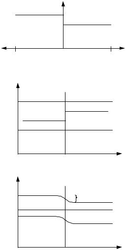
The pn junction is fundamental for constructing transistors and many other important applications. We assume a linear junction, which is abrupt, with acceptor doping for x < 0 and donor doping for x > 0 as in Fig. 6.17. Of course, this is an approximation. No doping profile is absolutely sharp. In some cases a graded junction (discussed later) may be a better approximation. We now develop approximately valid results concerning the pn junction. We use simple principles and develop what we call device equations.
6.3 Semiconductor Device Physics |
329 |
|
|
Na
Nd
p-region n-region
Fig. 6.17. Model of doping profile of abrupt pn junction
Electron |
p |
n |
|
Energy |
|
|
CB |
|
EF |
|
|
|
EF |
|
|
|
|
|
VB |
|
x = 0 |
|
x |
|
|
|
|
(a) |
|
|
Electron |
p |
n |
|
Energy |
|
|
|
|
|e |
φ| |
CB |
|
|
|
|
|
|
EF |
|
|
|
VB |
|
x = 0 |
|
x |
|
|
|
|
(b) |
|
|
Fig. 6.18. The pn junction: (a) Hypothetical junction just after doping but before equilibrium (i.e. before electrons and holes are transferred). (b) pn junction in equilibrium. CB = conduction band, VB = valence band
For x < −dp we assume p = Na and for x > +dn we assume p = Nd, i.e. exhaustion in both cases. Near the junction at x = 0, holes will tend to diffuse into the x > 0 region and electrons will tend to diffuse into the x < 0 region. This will cause a built-in potential that will be higher on the n-side (x > 0) than the p-side (x < 0). The potential will increase until it is of sufficient size to stop the net diffusion of electrons to the p-side and holes to the n-side. See Fig. 6.18. The region between
−dp and dn is called the depletion region. We further make the depletion layer approximation that assumes there are negligible free carriers in this depletion region. We assume this occurs because the large electric field in the region quickly sweeps any free carriers across it. It is fairly easy to calculate the built-in potential from the fact that the net hole (or electron) current is zero.
Consider, for example, the hole current:
|
dp |
= 0 . |
(6.159) |
J p = e pμp E − Dp |
|
|
dx |
|
|
The electric field is related to the potential by E = −dφ/dx, and using the Einstein relation, Dp = μpkT/e, we find
− kTe dϕ = dpp .
Integrating from −dp to dn, we find
p p |
0 |
|
e |
|
|
= exp |
|
(ϕn −ϕp |
pn0 |
|
kT |
|
where pp0 and pn0 mean the hole concentrations located in the homogeneous part
of the semiconductor beyond the depletion region. The Law of Mass Action tells us that np = ni2, and we know that pp0 = Na, nn0 = Nd, and nn0pn0 = ni2; so
pn0 = ni2  N
N
Thus, we find
e(ϕn −ϕp ) = kTln
for the built-in potential. The same built-in potential results from the constancy of the chemical potential. We will leave this as a problem.
We obtain the width of the depletion region by solving Gauss’s law for this region. We have assumed negligible carriers in the depletion region −dp to dn:
|
|
|
|
|
|
|
|
|
|
|
|
|
dE |
|
= − |
eNa |
|
for |
− d p ≤ x ≤ 0 , |
(6.164) |
|
dx |
|
ε |
|
|
|
|
|
|
|
and |
|
|
|
|
|
|
|
|
|
|
dE |
= + |
eNd |
for |
0 ≤ x ≤ dn . |
(6.165) |
|
|
dx |
|
ε |
|
|
|
|
|
|
|
|
6.3 Semiconductor Device Physics |
331 |
|
|
Integrating and using E = 0 at both edges of the depletion region
E = − |
eNa |
(x + d p ) |
for |
− d p ≤ x ≤ 0 , |
(6.166) |
|
ε |
|
|
|
|
|
|
|
E = + |
eNd |
(x − dn ) |
for |
0 ≤ x ≤ dn . |
(6.167) |
|
|
|
ε |
|
|
|
|
|
Since E must be continuous at x = 0, we find |
|
|
|
|
|
|
Nad p = Nd dn , |
(6.168) |
which is just an expression of charge neutrality. Using E = −dφ/dx, integrating these equations one more time, and using the fact that φ is continuous at x = 0, we find
|
ϕ =ϕ(dn ) −ϕ(−d p ) = |
e |
[Nd dn2 + Nad 2p ]. |
(6.169) |
|
2ε |
|
|
|
|
Using the electrical neutrality condition, Nadp = Nddn, we find
d p = |
|
2ε |
|
Nd |
|
, |
(6.170) |
ϕ |
|
|
|
|
|
eNa |
Na + Nd |
|
|
dn = |
|
2ε |
|
Na |
|
, |
(6.171) |
ϕ |
|
|
|
|
|
eNd |
Nd + Na |
|
|
and the width of the depletion region is W = dp + dn. Notice dp increases as Na decreases, as would be expected from electrical neutrality. Similar comments about dn and Nd may be made.
6.3.4 Depletion Width, Varactors, and Graded Junctions (EE)
From the previous results, we can show for the depletion width at an abrupt pn- junction
|
2ε |
ϕ |
|
|
|
W = |
|
Na + Nd |
(6.172) |
|
|
|
. |
|
e |
|
|
Na Nd |
|
Also,
|
|
Na |
|
|
|
dn = |
|
|
|
(6.173) |
|
|
|
W , |
|
Nd + Na |
|
|
|
Nd |
|
|
|
d p = |
|
|
|
(6.174) |
|
|
|
W . |
|
Nd + Na |
|
If we add a bias voltage φb selected so φb > 0 when a positive bias is applied on the p-side, then
|
2ε( ϕ −ϕb ) |
|
|
|
W = |
|
Na + Nd |
(6.175) |
|
|
. |
|
e |
|
Na Nd |
|
For noninfinite current, φ > φb.
The charge associated with the space charge on the p-side is Q = eAdpNa, where A is the cross-sectional area of the pn-junction. We find
|
Q = A 2eε( p −ϕb ) |
|
Na Nd |
. |
(6.176) |
|
Na + Nd |
|
|
|
|
|
|
|
|
|
|
The junction capacitance is then defined as |
|
|
|
|
|
|
|
|
dQ |
|
|
|
|
|
CJ = |
, |
|
|
(6.177) |
|
|
|
|
|
|
|
|
dϕb |
|
|
|
|
|
|
|
which, perhaps, not surprisingly comes out |
|
|
|
|
|
|
|
CJ = |
|
εA |
|
, |
|
|
|
(6.178) |
|
|
W |
|
|
|
|
|
|
|
|
|
|
|
|
just like a parallel-plate capacitor. Note that CJ depends on the voltage through W. When the pn-junction is used in such a way as to make use of the voltage dependence of CJ, the resulting device is called a varactor. A varactor is useful when it is desired to vary the capacitance electronically rather than mechanically.
To introduce another kind of pn-junction, and to see how this affects the concept of a varactor, let us consider the graded junction. Any simple model of a junction only approximately describes reality. This is true for both abrupt and graded junctions. The abrupt model may approximate an alloyed junction. When the junction is formed by diffusion, it may be better described by a graded junction. For a graded junction, we assume
which is p-type for x < 0 and n-type for x > 0. Note the variation is now smooth rather than abrupt. We assume, as before, that within the transition region we have
6.3 Semiconductor Device Physics |
333 |
|
|
complete ionization of impurities and that carriers there can be neglected in terms of their effect on net charge. Gauss’ law becomes
dE |
= |
e |
(Nd − Na ) = |
eGx |
|
dz |
|
ε . |
(6.180) |
ε |
Integrating |
|
|
|
|
|
|
|
|
E = eG x2 |
+ k . |
|
(6.181) |
|
|
|
2ε |
|
|
|
The doping is symmetrical, so the electric field should vanish at the same distance on either side from x = 0. Therefore,
|
|
|
d p = dn = W |
, |
|
|
|
|
|
|
|
|
|
|
|
|
|
2 |
|
|
|
|
|
and |
|
|
|
|
|
|
|
|
|
|
|
|
|
|
|
|
|
|
eG |
|
|
2 |
W |
2 |
|
|
|
E = |
x |
. |
|
|
|
2ε |
|
|
|
− |
|
|
|
|
|
|
|
|
|
|
|
2 |
|
|
|
|
|
|
|
|
|
|
|
|
|
|
|
|
|
|
|
|
Integrating |
|
|
|
|
|
|
|
|
|
|
|
|
|
|
|
|
|
|
eG |
x3 |
W |
2 |
|
|
ϕ(z) = − |
2ε |
|
|
|
|
|
− |
|
|
x |
+ k2 . |
|
3 |
|
|
|
|
|
|
|
|
|
2 |
|
|
|
|
|
|
|
|
|
|
|
|
|
|
|
|
|
|
|
|
Thus, |
|
|
|
|
|
|
|
|
|
|
|
|
|
|
|
|
W |
|
|
−W |
|
W 3 eG |
ϕ =ϕ |
|
2 −ϕ |
|
|
|
|
= |
|
12 |
ε , |
|
|
2 |
|
or
(6.182)
(6.183)
(6.184)
(6.185)
12ε |
1/ 3 |
W = |
eG |
ϕ . |
|
|
With an applied voltage, this becomes |
|
|
W = 12ε |
|
1/ 3 |
( ϕ −ϕb ) |
eG |
|
|
The charge associated with the right dipole layer is
Q = ∫ |
W / 2 |
eGxAdx = |
eGW 2 |
|
8 |
0 |
|
The junction capacitance therefore is
|
CJ = |
dQ |
|
= |
dQ |
|
|
dW |
|
, |
(6.189) |
|
dϕb |
dW |
dϕb |
|
|
|
|
|
|
|
|
|
|
|
|
which, finally, gives again
CJ = AWε .
But, now W depends on φb in a 1/3 power way rather than a 1/2 power. Different approximate models lead to different approximate device equations.
6.3.5 Metal Semiconductor Junctions — the Schottky Barrier (EE)
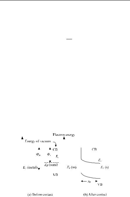
We consider the situation shown in Fig. 6.19 where an n-type semiconductor is in contact with the metal. Before contact we assume the Fermi level of the semiconductor is above the Fermi level of the metal. After contact electrons flow from the semiconductor to the metal and the Fermi levels equalize. The work functions Φm, Φs are defined in Fig. 6.19. We assume Φm > Φs. If Φm < Φs an ohmic contact with a much smaller barrier is formed (Streetman [6.40, p185ff]). The internal electric fields cause a varying potential and hence band bending as shown. The concept of band bending requires the semiclassical approximation (Sect. 6.1.4). Let us analyze this in a bit more detail. Choose x > 0 in the semiconductor and x < 0 in the metal. We assume the depletion layer has width xb. For xb > x > 0, Gauss’ equation is
Fig. 6.19. Schottky barrier formation (sketch)
6.3 Semiconductor Device Physics 335
Using E = −dφ/dx, setting the potential at 0 and xb equal to φ0 and φxb, and requiring the electric field to vanish at x = xb, by integrating the above for φ we find
|
|
|
N |
d |
ex2 |
|
ϕ0 −ϕx |
b |
= − |
|
b |
. |
(6.191) |
|
|
|
|
|
|
2ε |
|
If the potential energy difference for electrons across the barrier is |
|
V = −e(ϕ0 −ϕzb ) , |
|
we know |
|
|
|
|
|
|
|
V = +EF (s) − EF (m) |
(6.192) |
(before contact). |
|
Solving the above for xb gives the width of the depletion layer as |
|
x = |
2ε |
V . |
(6.193) |
b |
|
Nd e2 |
|
|
|
|
|
|
|
|
Shottky barrier diodes have been used as high-voltage rectifiers. The behavior of these diodes can be complicated by “dangling bonds” where the rough semiconductor surface joins the metal. See Bardeen [6.3].
6.3.6 Semiconductor Surface States and Passivation (EE)
The subject of passivation is complex, and we will only make brief comments. The most familiar passivation layer is SiO2 over Si, which reduces the number of surface states. A mixed layer of GaAs-AlAs on GaAs is also a passivating layer that reduces the number of surface states. The ease of passivation of the Si surface by oxygen is a major reason it is the dominant semiconductor for device usage.
CB |
CB |
Donor |
Donor |
EF |
EF |
VB |
VB |
(a) |
(b) |
Fig. 6.20. p-type semiconductor with donor surface states (a) before equilibrium, (b) after equilibrium (T = 0). In both (a) and (b) only relative energies are sketched