

ADSP-BF535
The powerful 40-bit shifter has extensive capabilities for performing shifting, rotating, normalization, extraction, and for depositing data.
The data for the computational units is found in a multiported register file of sixteen 16-bit entries or eight 32-bit entries.
A powerful program sequencer controls the flow of instruction execution, including instruction alignment and decoding. The sequencer supports conditional jumps and subroutine calls, as well as zero-overhead looping. A loop buffer stores instructions locally, eliminating instruction memory accesses for tightly looped code.
Two data address generators (DAGs) provide addresses for simultaneous dual operand fetches from memory. The DAGs share a register file containing four sets of 32-bit Index, Modify, Length, and Base registers. Eight additional 32-bit registers provide pointers for general indexing of variables and stack locations.
Blackfin processors support a modified Harvard architecture in combination with a hierarchical memory structure. Level 1 (L1) memories are those that typically operate at the full processor speed with little or no latency. Level 2 (L2) memories are other memories, on-chip or off-chip, that may take multiple processor cycles to access. At the L1 level, the instruction memory holds instructions only. The two data memories hold data, and a dedicated scratch pad data memory stores stack and local variable information. At the L2 level, there is a single unified memory space, holding both instructions and data.
In addition, the L1 instruction memory and L1 data memories may be configured as either Static RAMs (SRAMs) or caches. The Memory Management Unit (MMU) provides memory protection for individual tasks that may be operating on the core and may protect system registers from unintended access.
The architecture provides three modes of operation: user mode, supervisor mode, and Emulation mode. User mode has restricted access to certain system resources, thus providing a protected software environment, while supervisor mode has unrestricted access to the system and core resources.
The Blackfin processor instruction set has been optimized so that 16-bit op-codes represent the most frequently used instructions, resulting in excellent compiled code density. Complex DSP instructions are encoded into 32-bit op-codes, representing fully featured multifunction instructions. Blackfin processors support a limited multiple issue capability, where a 32-bit instruction can be issued in parallel with two 16-bit instructions, allowing the programmer to use many of the core resources in a single instruction cycle.
The Blackfin processor assembly language uses an algebraic syntax for ease of coding and readability. The architecture has been optimized for use in conjunction with the C/C++ compiler, resulting in fast and efficient software implementations.
Memory Architecture
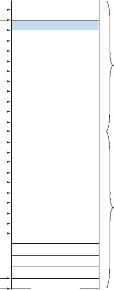
The ADSP-BF535 Blackfin processor views memory as a single unified 4 Gbyte address space, using 32-bit addresses. All resources, including internal memory, external memory, PCI
address spaces, and I/O control registers, occupy separate sections of this common address space. The memory portions of this address space are arranged in a hierarchical structure to provide a good cost/performance balance with very fast, low latency memory as cache or SRAM very close to the processor; and larger, lower cost, and lower performance memory systems farther away from the processor. See Figure 2.
0xFFFF FFFF 
 CORE MMR REGISTERS (2M BYTE)
0xFFE0 0000
SYSTEM MMR REGISTERS (2M BYTE)
0xFFC0 0000
|
|
|
|
|
|
|
|
|
|
|
RESERVED |
|
|
|
|
|
|
|
|
|
0xFFB0 1000 |
|
|
|
|
|
|
|
|
|
|
|
|
|
|
|
|
|
|
|
|
|
|
|
|
|
|
|
|
|
|
|
|
|
|
|
|
|
|
|
|
|
|
|
|
|
|
|
|
|
|
SCRATCHPAD SRAM (4K BYTE) |
|
|
|
|
|
|
|
||||
0xFFB0 0000 |
|
|
|
|
|
|
|
|
|
|
|
|
|
|
|
|
|
|
|
MAP |
|
|
|
|
|
|
|
|
|
|
|
RESERVED |
|
|
|
|
|
|
|
|
|
|
|
|
|
|
|
|
|
|
|
|
|
|
|
|
|
|
|
|
|
|
0xFFA0 4000 |
|
|
|
|
|
|
|
|
|
|
|
|
|
|
|
|
|
|
|
MEMORY |
|
|
|
|
|
|
|
|
|
|
|
|
|
|
|
|
|
|
|
|
|
|
|
|
|
|
|
|
|
|
|
|
RESERVED |
|
|
|
|
|||||
|
|
|
|
|
|
|
|
|
INSTRUCTION SRAM (16K BYTE) |
|
|
|
|
|
||||||
0xFFA0 0000 |
|
|
|
|
|
|
|
|
|
|
|
|
|
|
|
|
|
|
|
INTERNAL |
0xFF90 4000 |
|
|
|
|
|
|
|
|
|
|
|
|
|
|
|
|
|
|
|
|
|
|
|
|
|
|
|
|
|
|
RESERVED |
||||||||||
|
|
|
|
|
|
|
|
|
|
|
|
|
|
|
|
|
|
|
|
|
|
|
|
|
|
|
|
|
|
|
|
|
|
|
|
|
|
|
|||
|
|
|
|
|
|
|
|
DATA BANK B SRAM (16K BYTE) |
|
|
|
|
|
|
||||||
0xFF90 0000 |
|
|
|
|
|
|
|
|
|
|
|
|
|
|
|
|
|
|
|
|
0xFF80 4000 |
|
|
|
|
|
|
|
|
|
|
|
|
|
|
|
|
|
|
|
|
|
|
|
|
|
|
|
|
|
|
|
|
|
|
|
|
|
|
|
|
|
|
|
|
|
|
|
|
|
|
|
|
|
|
|
|
|
|
|
|
||
|
|
|
|
|
|
|
|
DATA BANK A SRAM (16K BYTE) |
|
|
|
|
|
|
||||||
0xFF80 0000 |
|
|
|
|
|
|
|
|
|
|
|
|
|
|
|
|
|
|
|
|
|
|
|
|
|
|
|
|
|
|
|
RESERVED |
|
|
|
|
|
|
|
|
|
0xF003 FFFF |
|
|
|
|
|
|
|
|
|
|
|
|
|
|
|
|
|
|
|
|
|
|
|
|
|
|
|
|
|
|
|
|
|
|
|
|
|
|
|
||
|
|
|
|
|
|
|
|
|
L2 SRAM MEMORY (256K BYTE) |
|
|
|
|
|
|
|||||
0xF000 0000 |
|
|
|
|
|
|
|
|
|
|
|
|
|
|
|
|
|
|
|
|
|
|
|
|
|
|
|
|
|
|
|
RESERVED |
|
|
|
|
|
|
|
||
0xEF00 0000 |
|
|
|
|
|
|
|
|
|
|
|
|
|
|
|
|
|
|
|
|
|
|
|
|
|
|
|
|
|
|
|
|
|
||||||||
|
|
|
|
|
|
PCI CONFIG SPACE PORT (4 BYTE) |
|
|
|
|
||||||||||
0xEEFF FFFC |
|
|
|
|
|
|
|
|
|
|
|
|
|
|
|
|
|
|
|
|
|
|
|
|
|
|
|
|
|
|
|
|
|
||||||||
|
|
|
|
|
PCI CONFIG REGISTERS (64K BYTE) |
|
|
|
||||||||||||
0xEEFF FF00 |
|
|
|
|
|
|
|
|
|
|
|
|
|
|
|
|
|
|
|
|
0xEEFE FFFF |
|
|
|
|
|
|
|
|
|
|
RESERVED |
|
|
|
|
|
|
|||
|
|
|
|
|
|
|
|
|
|
|
|
|
|
|
|
|
|
|
|
|
|
|
|
|
|
|
|
|
|
|
|
|
|
|
|
|
|
|
|
||
|
|
|
|
|
|
|
|
|
|
|
|
|
|
|
||||||
|
|
|
|
|
|
|
|
|
|
PCI IO SPACE (64K BYTE) |
|
|
|
|
|
|||||
0xEEFE 0000 |
|
|
|
|
|
|
|
|
|
|
|
|
|
|
|
|
|
|
|
|
0xE7FF FFFF |
|
|
|
|
|
|
|
|
|
|
RESERVED |
|
|
|
|
|
||||
|
|
|
|
|
|
|
|
|
|
|
|
|
|
|
|
|
|
|
MAP |
|
|
|
|
|
|
|
|
|
|
|
|
|
|
|
|
|
|
|
|
|
|
|
|
|
|
|
|
PCI MEMORY SPACE (128M BYTE) |
|
|
|
|
||||||||||
|
|
|
|
|
|
|
|
|
|
|||||||||||
0xE000 0000 |
|
|
|
|
|
|
|
|
|
|
|
|
|
|
|
|
|
|
|
MEMORY |
|
|
|
|
|
ASYNC MEMORY BANK |
3 (64M BYTE) |
||||||||||||||
0x2FFF FFFF |
|
|
|
|
|
|
|
|
|
|
RESERVED |
|
|
|
|
|||||
0x2C00 0000 |
|
|
|
|
|
|
|
|
|
|
|
|
|
|
|
|
|
|
|
EXTERNAL |
|
|
|
|
|
|
|
|
|
|
|
|
|
|
|
|
|
|
|
||
|
|
|
|
|
|
|
|
|
|
|
|
|
|
|
|
|
|
|
||
|
|
|
|
|
ASYNC MEMORY BANK 2 (64M BYTE) |
|
|
|
||||||||||||
0x2800 0000 |
|
|
|
|
|
|
|
|
|
|
|
|
|
|
|
|
|
|
|
|
|
|
|
|
|
|
|
|
|
|
|
|
|
|
|
|
|
|
|||
0x2400 0000 |
|
|
|
|
ASYNC MEMORY BANK 1 (64M BYTE) |
|
|
|||||||||||||
|
|
|
|
|
|
|
|
|
|
|
|
|
|
|
|
|
|
|
|
|
|
|
|
|
|
|
|
|
|
|
|
|
|
|
|
|
|
|
|||
ASYNC MEMORY BANK 0 (64M BYTE)
0x2000 0000  SDRAM MEMORY BANK 3
(16M BYTE - 128M BYTE)1
0x1800 0000  SDRAM MEMORY BANK 2
(16M BYTE - 128M BYTE)1
0x1000 0000  SDRAM MEMORY BANK 1
(16M BYTE - 128M BYTE)1
0x0800 0000
SDRAM MEMORY BANK 0
(16M BYTE - 128M BYTE)1
0x0000 0000
1 THE ADDRESSES SHOWN FOR THE SDRAM BANKS REFLECT A FULLY POPULATED SDRAM ARRAY WITH 512M BYTES OF MEMORY. IF ANY BANK CONTAINS LESS THAN 128M BYTES OF MEMORY, THAT BANK WOULD EXTEND ONLY TO THE LENGTH OF THE REAL MEMORY SYSTEMS, AND THE END ADDRESS WOULD BECOME THE START ADDRESS OF THE NEXT BANK. THIS WOULD CONTINUE FOR ALL FOUR BANKS, WITH ANY REMAINING SPACE BETWEEN THE END OF MEMORY BANK 3 AND THE BEGINNING OF ASYNC MEMORY BANK 0, AT ADDRESS 0x2000 0000, TREATED AS RESERVED ADDRESS SPACE.
Figure 2. Internal/External Memory Map
–4– |
REV. A |

ADSP-BF535
The L1 memory system is the primary highest performance memory available to the Blackfin processor core. The L2 memory provides additional capacity with slightly lower performance. Lastly, the off-chip memory system, accessed through the External Bus Interface Unit (EBIU), provides expansion with SDRAM, flash memory, and SRAM, optionally accessing more than 768M bytes of external physical memory.
The memory DMA controller provides high bandwidth datamovement capability. It can perform block transfers of code or data between the internal L1/L2 memories and the external memory spaces (including PCI memory space).
Internal (On-Chip) Memory
The ADSP-BF535 Blackfin processor has four blocks of on-chip memory providing high bandwidth access to the core.
The first is the L1 instruction memory consisting of 16K bytes of 4-Way set-associative cache memory. In addition, the memory may be configured as an SRAM. This memory is accessed at full processor speed.
The second on-chip memory block is the L1 data memory, consisting of two banks of 16K bytes each. Each L1 data memory bank can be configured as one Way of a 2-Way set-associative cache or as an SRAM, and is accessed at full speed by the core.
The third memory block is a 4K byte scratch pad RAM which runs at the same speed as the L1 memories, but is only accessible as data SRAM (it cannot be configured as cache memory and is not accessible via DMA).
The fourth on-chip memory system is the L2 SRAM memory array which provides 256K bytes of high speed SRAM at the full bandwidth of the core, and slightly longer latency than the L1 memory banks. The L2 memory is a unified instruction and data memory and can hold any mixture of code and data required by the system design.
The Blackfin processor core has a dedicated low latency 64-bit wide datapath port into the L2 SRAM memory.
External (Off-Chip) Memory
External memory is accessed via the External Bus Interface Unit (EBIU). This interface provides a glueless connection to up to four banks of synchronous DRAM (SDRAM) as well as up to four banks of asynchronous memory devices including flash, EPROM, ROM, SRAM, and memory-mapped I/O devices.
The PC133 compliant SDRAM controller can be programmed to interface to up to four banks of SDRAM, with each bank containing between 16M bytes and 128M bytes providing access to up to 512M bytes of SDRAM. Each bank is independently programmable and is contiguous with adjacent banks regardless of the sizes of the different banks or their placement. This allows flexible configuration and upgradability of system memory while allowing the core to view all SDRAM as a single, contiguous, physical address space.
The asynchronous memory controller can also be programmed to control up to four banks of devices with very flexible timing parameters for a wide variety of devices. Each bank occupies a
64 Mbyte segment regardless of the size of the devices used so that these banks will only be contiguous if fully populated with 64M bytes of memory.
PCI
The PCI bus defines three separate address spaces, which are accessed through windows in the ADSP-BF535 Blackfin processor memory space. These spaces are PCI memory, PCI I/O, and PCI configuration.
In addition, the PCI interface can either be used as a bridge from the processor core as the controlling CPU in the system, or as a host port where another CPU in the system is the host and the ADSP-BF535 is functioning as an intelligent I/O device on the PCI bus.
When the ADSP-BF535 Blackfin processor acts as the system controller, it views the PCI address spaces through its mapped windows and can initialize all devices in the system and maintain a map of the topology of the environment.
The PCI memory region is a 4 Gbyte space that appears on the PCI bus and can be used to map memory I/O devices on the bus. The ADSP-BF535 Blackfin processor uses a 128 Mbyte window in memory space to see a portion of the PCI memory space. A base address register is provided to position this window anywhere in the 4 Gbyte PCI memory space while its position with respect to the processor addresses remains fixed.
The PCI I/O region is also a 4 Gbyte space. However, most systems and I/O devices only use a 64 Kbyte subset of this space for I/O mapped addresses. The ADSP-BF535 Blackfin processor implements a 64K byte window into this space along with a base address register which can be used to position it anywhere in the PCI I/O address space, while the window remains at the same address in the processor's address space.
PCI configuration space is a limited address space, which is used for system enumeration and initialization. This address space is a very low performance communication mode between the processor and PCI devices. The ADSP-BF535 Blackfin processor provides a one-value window to access a single data value at any address in PCI configuration space. This window is fixed and receives the address of the value, and the value if the operation is a write. Otherwise, the device returns the value into the same address on a read operation.
I/O Memory Space
Blackfin processors do not define a separate I/O space. All resources are mapped through the flat 32-bit address space. On-chip I/O devices have their control registers mapped into memory-mapped registers (MMRs) at addresses near the top of the 4 Gbyte address space. These are separated into two smaller blocks, one which contains the control MMRs for all core functions, and the other which contains the registers needed for setup and control of the on-chip peripherals outside of the core. The core MMRs are accessible only by the core and only in supervisor mode and appear as reserved space by on-chip peripherals, as well as external devices accessing resources through the PCI bus. The system MMRs are accessible by the core in supervisor mode and can be mapped as either visible or reserved to other devices, depending on the system protection model desired.
REV. A |
–5– |