- •TABLE OF CONTENTS
- •GENERAL DESCRIPTION
- •Portable Low Power Architecture
- •System Integration
- •ADSP-BF535 Peripherals
- •Processor Core
- •Figure 1. Processor Core
- •Memory Architecture
- •Figure 2. Internal/External Memory Map
- •Internal (On-Chip) Memory
- •External (Off-Chip) Memory
- •I/O Memory Space
- •Booting
- •Event Handling
- •Core Event Controller (CEC)
- •System Interrupt Controller (SIC)
- •Event Control
- •DMA Controllers
- •External Memory Control
- •PC133 SDRAM Controller
- •Asynchronous Controller
- •PCI Interface
- •PCI Host Function
- •PCI Target Function
- •USB Device
- •Real-Time Clock
- •Figure 3. External Components for RTC
- •Watchdog Timer
- •Timers
- •Serial Ports (Sports)
- •Serial Peripheral Interface (SPI) Ports
- •Figure 4. SPI Clock Rate Calculation
- •UART Port
- •Figure 5. UART Clock Rate Calculation
- •Programmable Flags (PFX)
- •Dynamic Power Management
- •Mode Transitions
- •Figure 6. Mode Transitions
- •Power Savings
- •Peripheral Power Control
- •Clock Signals
- •Figure 7. Clock Ratio Example
- •Booting Modes
- •Instruction Set Description
- •Development Tools
- •EZ-KIT Lite™ for ADSP-BF535 Blackfin Processor
- •Designing an Emulator Compatible Processor Board (Target)
- •Additional Information
- •PIN DESCRIPTIONS
- •Unused Pins
- •SPECIFICATIONS
- •Recommended Operating Conditions
- •ABSOLUTE MAXIMUM RATINGS
- •ESD SENSITIVITY
- •TIMING SPECIFICATIONS
- •Clock and Reset Timing
- •Figure 8. Clock and Reset Timing
- •Programmable Flags Cycle Timing
- •Figure 9. Programmable Flags Cycle Timing
- •Timer PWM_OUT Cycle Timing
- •Figure 10. Timer PWM_OUT Cycle Timing
- •Asynchronous Memory Write Cycle Timing
- •Figure 11. Asynchronous Memory Write Cycle Timing
- •Asynchronous Memory Read Cycle Timing
- •Figure 12. Asynchronous Memory Read Cycle Timing
- •SDRAM Interface Timing
- •Figure 13. SDRAM Interface Timing
- •Serial Ports
- •Figure 14. Serial Ports
- •Serial Peripheral Interface (SPI) Port —Master Timing
- •Figure 15. Serial Peripheral Interface (SPI) Port—Master Timing
- •Serial Peripheral Interface (SPI) Port —Slave Timing
- •Figure 16. Serial Peripheral Interface (SPI) Port—Slave Timing
- •Universal Asynchronous Receiver-Transmitter (UART) Port—Receive and Transmit Timing
- •Figure 17. UART Port—Receive and Transmit Timing
- •JTAG Test and Emulation Port Timing
- •Figure 18. JTAG Port Timing
- •Output Drive Currents
- •Figure 19. Output Drive Current
- •Figure 20. PCI 33 MHz Output Drive Current
- •Figure 21. PCI_REQ Output Drive Current
- •Power Dissipation
- •Test Conditions
- •Output Enable Time
- •Output Disable Time
- •Example System Hold Time Calculation
- •Figure 22. Output Enable/Disable
- •Figure 23. Equivalent Device Loading for AC Measurements (Includes All Fixtures)
- •Figure 24. Voltage Reference Levels for AC Measurements (Except Output Enable/Disable)
- •Environmental Conditions
- •260-Ball PBGA Pinout
- •Figure 25. 260-Ball Metric PBGA Pin Configuration (Top View)
- •Figure 26. 260-Ball Metric PBGA Pin Configuration (Bottom View)
- •OUTLINE DIMENSIONS
- •Figure 27. 260-Ball Metric Plastic Ball Grid Array (PBGA) (B-260)
- •ORDERING GUIDE
- •Revision History
ADSP-BF535
JTAG Test and Emulation Port Timing
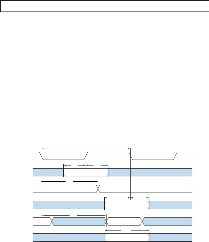
Table 25 and Figure 18 describe JTAG port operations.
Table 25. JTAG Port Timing
Parameter |
|
Min |
Max |
Unit |
|
|
|
|
|
Timing Requirements |
|
|
|
|
tTCK |
TCK Period |
20.0 |
|
ns |
tSTAP |
TDI, TMS Setup Before TCK High |
|
4.0 |
ns |
tHTAP |
TDI, TMS Hold After TCK High |
|
4.0 |
ns |
tSSYS |
System Inputs Setup Before TCK Low1 |
|
4.0 |
ns |
tHSYS |
System Inputs Hold After TCK Low1 |
|
5.0 |
ns |
tTRSTW |
TRST Pulse Width2 |
4.0 |
|
ns |
Switching Characteristics |
|
|
|
|
tDTDO |
TDO Delay from TCK Low |
|
7.0 |
ns |
tDSYS |
System Outputs Delay After TCK Low3 |
0.0 |
15.0 |
ns |
1System Inputs=DATA31-0, ADDR25-2, ARDY, TMR2-0, PF15-0, RSCLK0, RFS0, DR0, TSCLK0, TFS0, RSCLK1, RFS1, DR1, TSCLK1, TFS1, MOSI0, MISO0, SCK0, MOSI1, MISO1, SCK1, RX0, RX1, USB_CLK, XVER_DATA, DPLS, DMNS, NMI, RESET, BYPASS, BMODE2-0, PCI_AD31-0, PCI_CBE3-0, PCI_FRAME, PCI_IRDY, PCI_TRDY, PCI_DEVSEL, PCI_STOP, PCI_PERR, PCI_PAR, PCI_SERR, PCI_RST, PCI_GNT, PCI_IDSEL, PCI_LOCK, PCI_CLK, PCI_INTA, PCI_INTB, PCI_INTC, PCI_INTD.
250 MHz max.
3System Outputs=DATA31-0, ADDR25-2, ABE3-0/SDQM3-0, AOE, ARE, AWE, SCAS, CLKOUT/SCLK1, SCLK0, SCKE, SA10, SWE, SMS3-0,
SRAS, TMR2-0, PF15-0, RSCLK0, RFS0, TSCLK0, TFS0, DT0, RSCLK1, RFS1, TSCLK1, TFS1, DT1, MOSI0, MISO0, SCK0, MOSI1, MISO1, |
||
SCK1, TX0, TX1, TXDPLS, TXDMNS, TXEN, SUSPEND, DEEPSLEEP, PCI_AD31-0, PCI_CBE3-0, PCI_FRAME, PCI_IRDY, PCI_TRDY, |
||
PCI_DEVSEL, PCI_STOP, PCI_PERR, PCI_PAR, PCI_REQ, PCI_SERR, PCI_RST, PCI_INTA, EMU. |
||
|
tT C K |
|
TC K |
|
|
tS T A P |
tH T A P |
|
TM S |
|
|
TD I |
|
|
tD T D O |
|
|
T D O |
|
|
|
tS S Y S |
tH S Y S |
S YS TE M |
|
|
IN P U TS |
|
|
tD SY S |
|
|
SY S TE M |
|
|
O U TP U TS |
|
|
|
|
tT R S T W |
T R S T
Figure 18. JTAG Port Timing
REV. A |
–35– |