

Добавил:
Upload
Опубликованный материал нарушает ваши авторские права? Сообщите нам.
Вуз:
Предмет:
Файл:
ADSP-BF535
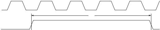
Timer PWM_OUT Cycle Timing
Table 13 and Figure 10 describe timer expired operations. The input signal is asynchronous in “width capture mode” and has an absolute maximum input frequency of fSCLK 2.
Table 13. Timer PWM_OUT Cycle Timing
Parameter |
|
Min |
Max |
Unit |
|
|
|
|
|
Switching Characteristics |
|
|
|
|
tHTO |
Timer Pulse Width Output1 |
7.5 |
(232–1) cycles |
ns |
1 The minimum time for tHTO is one cycle, and the maximum time for tHTO equals (232–1) cycles.
SCLK
tHTO
PWM_OUT
Figure 10. Timer PWM_OUT Cycle Timing
–26– |
REV. A |