- •TABLE OF CONTENTS
- •GENERAL DESCRIPTION
- •Portable Low Power Architecture
- •System Integration
- •ADSP-BF535 Peripherals
- •Processor Core
- •Figure 1. Processor Core
- •Memory Architecture
- •Figure 2. Internal/External Memory Map
- •Internal (On-Chip) Memory
- •External (Off-Chip) Memory
- •I/O Memory Space
- •Booting
- •Event Handling
- •Core Event Controller (CEC)
- •System Interrupt Controller (SIC)
- •Event Control
- •DMA Controllers
- •External Memory Control
- •PC133 SDRAM Controller
- •Asynchronous Controller
- •PCI Interface
- •PCI Host Function
- •PCI Target Function
- •USB Device
- •Real-Time Clock
- •Figure 3. External Components for RTC
- •Watchdog Timer
- •Timers
- •Serial Ports (Sports)
- •Serial Peripheral Interface (SPI) Ports
- •Figure 4. SPI Clock Rate Calculation
- •UART Port
- •Figure 5. UART Clock Rate Calculation
- •Programmable Flags (PFX)
- •Dynamic Power Management
- •Mode Transitions
- •Figure 6. Mode Transitions
- •Power Savings
- •Peripheral Power Control
- •Clock Signals
- •Figure 7. Clock Ratio Example
- •Booting Modes
- •Instruction Set Description
- •Development Tools
- •EZ-KIT Lite™ for ADSP-BF535 Blackfin Processor
- •Designing an Emulator Compatible Processor Board (Target)
- •Additional Information
- •PIN DESCRIPTIONS
- •Unused Pins
- •SPECIFICATIONS
- •Recommended Operating Conditions
- •ABSOLUTE MAXIMUM RATINGS
- •ESD SENSITIVITY
- •TIMING SPECIFICATIONS
- •Clock and Reset Timing
- •Figure 8. Clock and Reset Timing
- •Programmable Flags Cycle Timing
- •Figure 9. Programmable Flags Cycle Timing
- •Timer PWM_OUT Cycle Timing
- •Figure 10. Timer PWM_OUT Cycle Timing
- •Asynchronous Memory Write Cycle Timing
- •Figure 11. Asynchronous Memory Write Cycle Timing
- •Asynchronous Memory Read Cycle Timing
- •Figure 12. Asynchronous Memory Read Cycle Timing
- •SDRAM Interface Timing
- •Figure 13. SDRAM Interface Timing
- •Serial Ports
- •Figure 14. Serial Ports
- •Serial Peripheral Interface (SPI) Port —Master Timing
- •Figure 15. Serial Peripheral Interface (SPI) Port—Master Timing
- •Serial Peripheral Interface (SPI) Port —Slave Timing
- •Figure 16. Serial Peripheral Interface (SPI) Port—Slave Timing
- •Universal Asynchronous Receiver-Transmitter (UART) Port—Receive and Transmit Timing
- •Figure 17. UART Port—Receive and Transmit Timing
- •JTAG Test and Emulation Port Timing
- •Figure 18. JTAG Port Timing
- •Output Drive Currents
- •Figure 19. Output Drive Current
- •Figure 20. PCI 33 MHz Output Drive Current
- •Figure 21. PCI_REQ Output Drive Current
- •Power Dissipation
- •Test Conditions
- •Output Enable Time
- •Output Disable Time
- •Example System Hold Time Calculation
- •Figure 22. Output Enable/Disable
- •Figure 23. Equivalent Device Loading for AC Measurements (Includes All Fixtures)
- •Figure 24. Voltage Reference Levels for AC Measurements (Except Output Enable/Disable)
- •Environmental Conditions
- •260-Ball PBGA Pinout
- •Figure 25. 260-Ball Metric PBGA Pin Configuration (Top View)
- •Figure 26. 260-Ball Metric PBGA Pin Configuration (Bottom View)
- •OUTLINE DIMENSIONS
- •Figure 27. 260-Ball Metric Plastic Ball Grid Array (PBGA) (B-260)
- •ORDERING GUIDE
- •Revision History
ADSP-BF535
Clock and Reset Timing
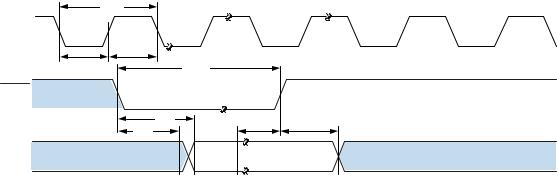
Table 11 and Figure 8 describe clock and reset operations. Per ABSOLUTE MAXIMUM RATINGS on Page 22, combinations of CLKIN and clock multipliers must not select core and system clocks in excess of 350/300/200 MHz and 133 MHz, respectively.
Table 11. Clock and Reset Timing
Parameter |
|
Min |
Max |
Unit |
|
|
|
|
|
Timing Requirements |
|
|
|
|
tCKIN |
CLKIN Period |
25.0 |
100.0 |
ns |
tCKINL |
CLKIN Low Pulse1 |
10.0 |
|
ns |
tCKINH |
CLKIN High Pulse1 |
10.0 |
|
ns |
tWRST |
RESET Asserted Pulse Width Low2 |
11 tCKIN |
|
ns |
tMSD |
Delay from RESET Asserted to MSELx, SSELx, BYPASS, |
|
15.0 |
ns |
|
and DF Valid3 |
|
|
|
tMSS |
MSELx/SSELx/DF/BYPASS Stable Setup Before RESET |
2 tCKIN |
|
ns |
|
Deasserted4 |
|
|
|
tMSH |
MSELx/SSELx/DF/BYPASS Stable Hold After RESET |
2 tCKIN |
|
ns |
|
Deasserted |
|
|
|
Switching Characteristics |
|
|
|
|
tPFD |
Flag Output Disable Time After RESET Asserted |
|
15.0 |
ns |
|
|
|
|
|
1Applies to Bypass mode and Non-bypass mode.
2Applies after power-up sequence is complete. At power-up, the processor’s internal phase-locked loop requires no more than 2000 CLKIN cycles, while RESET is asserted, assuming stable power supplies and CLKIN (not including start-up time of external clock oscillator).
3SSELx, MSELx and DF values can change from this point, but the values must be valid.
4SSELx, MSELx and DF values must be held from this time, until the hold time expires.
tC K IN |
|
|
CLKIN |
|
|
tC K IN H |
|
|
tC K IN L |
tW R S T |
|
RESET |
|
|
tM S D |
tM S S |
tM S H |
tP F D |
|
|
SSEL1–0
MSEL6–0
BYPASS
DF
Figure 8. Clock and Reset Timing
–24– |
REV. A |