
- •CONTENTS
- •FIGURES
- •TABLES
- •1.1 Manual Contents
- •1.2 Notational Conventions and Terminology
- •1.3 Related Documents
- •1.4 Application Support Services
- •2.1 Typical Applications
- •2.2 Microcontroller Features
- •2.3 Functional Overview
- •2.3.1 Core
- •2.3.1.3 Register File
- •2.3.2 Memory Controller
- •2.4 Internal Timing
- •2.4.1 Clock and Power Management Logic
- •2.4.2 Internal Timing
- •2.4.2.1 Clock Failure Detection Logic
- •2.4.2.2 External Timing
- •2.4.2.3 Power Management Options
- •2.4.3 Internal Memory
- •2.4.4 Serial Debug Unit
- •2.4.5 Interrupt Service
- •2.5 Internal Peripherals
- •2.5.1 I/O Ports
- •2.5.2 Serial I/O (SIO) Port
- •2.5.3 Synchronous Serial I/O (SSIO) Port
- •2.5.4 Event Processor Array (EPA) and Timer/Counters
- •2.5.7 Stack Overflow Module
- •2.5.8 Watchdog Timer
- •2.6 Special Operating Modes
- •2.7 Chip Configuration Registers
- •3.1 Overview of the Instruction Set
- •3.1.1 BIT Operands
- •3.1.2 BYTE Operands
- •3.1.4 WORD Operands
- •3.1.5 INTEGER Operands
- •3.1.9 Converting Operands
- •3.1.10 Conditional Jumps
- •3.1.11 Floating-Point Operations
- •3.1.12 Extended Instructions
- •3.2 Addressing Modes
- •3.2.1 Direct Addressing
- •3.2.2 Immediate Addressing
- •3.2.3 Indirect Addressing
- •3.2.3.1 Extended Indirect Addressing
- •3.2.3.2 Indirect Addressing with Autoincrement
- •3.2.3.3 Extended Indirect Addressing with Autoincrement
- •3.2.3.4 Indirect Addressing with the Stack Pointer
- •3.2.4 Indexed Addressing
- •3.2.4.3 Extended Indexed Addressing
- •3.2.4.4 Zero-indexed Addressing
- •3.3 Considerations for Crossing Page Boundaries
- •3.4 Software Protection Features and Guidelines
- •4.1 Memory Map Overview
- •4.2 Memory Partitions
- •4.2.1 External Memory
- •4.2.2 Internal ROM
- •4.2.2.1 Program Memory in Page FFH
- •4.2.2.3 Reserved Memory Locations
- •4.2.2.4 Interrupt, PIH, and PTS Vectors
- •4.2.2.5 Chip Configuration Bytes
- •4.2.3 Internal RAM (Code RAM)
- •4.2.4.2 Peripheral SFRs
- •4.2.5 Register File
- •4.2.5.2 Stack Pointer (SP)
- •4.3 Windowing
- •4.3.1 Selecting a Window
- •4.3.2 Addressing a Location Through a Window
- •4.3.2.4 Unsupported Locations Windowing Example
- •4.3.2.5 Using the Linker Locator to Set Up a Window
- •4.3.3 Windowing and Addressing Modes
- •4.4 Controlling Read Access to the Internal ROM
- •4.5 Remapping Internal ROM
- •5.1 Functional Overview
- •5.2 Stack Operations
- •5.3 Stack Overflow Module Registers
- •5.4 Programming the Stack Overflow Module
- •5.4.1 Initializing the Stack Pointer
- •5.4.2 Enabling the Stack Overflow Module and Specifying Stack Boundaries
- •6.1 Overview of the Interrupt Control Circuitry
- •6.2 Interrupt Signals and Registers
- •6.3 Interrupt Sources, Priorities, and Vector Addresses
- •6.3.1 PIH Interrupt Sources, Priorities, and Vector Addresses
- •6.3.1.1 Using Software to Provide the Vector Address
- •6.3.1.2 Providing the Vector Address in Response to a CPU Request
- •6.3.2 Special Interrupts
- •6.3.2.1 Unimplemented Opcode
- •6.3.2.2 Software Trap
- •6.3.2.4 Stack Overflow
- •6.3.3 External Interrupt Signal
- •6.3.4 Shared Interrupt Requests
- •6.4 Interrupt Latency
- •6.4.1 Situations that Increase Interrupt Latency
- •6.4.2 Calculating Latency
- •6.4.2.2 PTS Interrupt Latency
- •6.5 Programming the Interrupts
- •6.5.1 Modifying Interrupt Priorities
- •6.5.2 Determining the Source of an Interrupt
- •6.6 Initializing the PTS Control Blocks
- •6.6.1 Specifying the PTS Count
- •6.6.2 Selecting the PTS Mode
- •6.6.3 Single Transfer Mode
- •6.6.4 Block Transfer Mode
- •6.6.5 Dummy Mode
- •7.1 I/O Ports Overview
- •7.2 Configuring the Port Pins
- •7.2.2 Configuring Ports 3 and 4 (Address/Data Bus)
- •7.2.3 Port Configuration Example
- •7.3.1 Address and Data Signals (Ports 3, 4, and EPORT)
- •7.3.1.1 EPORT Status During Reset, CCB Fetch, Idle, Powerdown, and Hold
- •7.3.5 External Interrupt Signal (Port 2)
- •7.3.6 PWM Signals (Port 11)
- •7.3.7 Serial I/O Port Signals (Ports 2 and 7)
- •7.3.8 Special Operating Mode Signal (Port 5 Pin 7)
- •7.3.9 Synchronous Serial I/O Port Signals (Port 10)
- •7.4 I/O Port Internal Structures
- •7.4.3 Internal Structure for Ports 3 and 4 (Address/Data Bus)
- •8.1 Serial I/O (SIO) Port Functional Overview
- •8.2 Serial I/O Port Signals and Registers
- •8.3 Serial Port Modes
- •8.3.1 Synchronous Mode (Mode 0)
- •8.3.2 Asynchronous Modes (Modes 1, 2, and 3)
- •8.3.2.1 Mode 1
- •8.3.2.2 Mode 2
- •8.3.2.3 Mode 3
- •8.3.2.4 Multiprocessor Communications
- •8.4 Programming the Serial Port
- •8.4.1 Configuring the Serial Port Pins
- •8.4.2 Programming the Control Register
- •8.4.3 Programming the Baud Rate and Clock Source
- •8.4.4 Enabling the Serial Port Interrupts
- •8.4.5 Determining Serial Port Status
- •CHAPTER 9 Synchronous Serial I/O (SSIO) Port
- •9.1 SSIO Port Overview
- •9.1.1 Standard Mode
- •9.1.2 Duplex Mode
- •9.2 SSIO pORT sIGNALS AND rEGISTERS
- •9.3 ssio Port Operation
- •9.3.1 Transmitting and Receiving Data
- •9.3.1.1 Normal Transfers (All Modes)
- •9.3.1.2 Handshaking Transfers (Standard Mode Only)
- •9.4 Programming the SSIO Port
- •9.4.1 Configuring the SSIO Port Pins
- •9.4.2 Configuring the SSIO Registers
- •9.4.2.1 The SSIO Baud (SSIO_BAUD) Register
- •9.4.2.3 The SSIO 0 Clock (SSIO0_CLK) Register
- •9.4.2.4 The SSIO 1 Clock (SSIO1_CLK) Register
- •9.4.3 Enabling the SSIO Interrupts
- •9.5 Programming Considerations
- •9.5.2 Standard Mode Considerations
- •9.5.3 Duplex Mode Considerations
- •10.1 PWM FUNCTIONAL OVERVIEW
- •10.2 PWM Signals and Registers
- •10.3 pwm operation
- •10.4 Programming the Frequency and Period
- •10.5 Programming the Duty Cycle
- •10.5.1 Sample Calculations
- •10.5.2 Reading the Current Value of the Down-counter
- •10.5.3 Enabling the PWM Outputs
- •10.5.4 Generating Analog Outputs
- •11.1 EPA Functional Overview
- •11.2 EPA and Timer/Counter Signals and Registers
- •11.3 Timer/Counter Functional Overview
- •11.3.1 Timer Multiplexing on the Time Bus
- •11.4 EPA Channel Functional Overview
- •11.4.1 Operating in Input Capture Mode
- •11.4.2 Operating in Output Compare Mode
- •11.4.3 Operating in Compare Mode with the Output/Simulcapture Channels
- •11.4.4 Generating a 32-bit Time Value
- •11.4.5 Controlling a Pair of Adjacent Pins
- •11.5 Programming the EPA and Timer/Counters
- •11.5.1 Configuring the EPA and Timer/Counter Signals
- •11.5.2 Programming the Timers
- •11.5.3 Programming the Capture/Compare Channels
- •11.5.4 Programming the Compare-only (Output/Simulcapture) Channels
- •11.6 Enabling the EPA Interrupts
- •11.7 Determining Event Status
- •CHAPTER 12 Analog-to-digital (A/D) Converter
- •12.1 A/D Converter Functional Overview
- •12.2 A/D Converter Signals and Registers
- •12.3 A/D Converter Operation
- •12.4 Programming the A/D Converter
- •12.4.1 Programming the A/D Test Register
- •12.4.2 Programming the A/D Result Register (for Threshold Detection Only)
- •12.4.3 Programming the A/D Time Register
- •12.4.4 Programming the A/D Command Register
- •12.4.5 Programming the A/D Scan Register
- •12.4.6 Enabling the A/D Interrupt
- •12.5 Determining A/D Status and Conversion Results
- •12.6 Design Considerations
- •12.6.1 Designing External Interface Circuitry
- •12.6.1.1 Minimizing the Effect of High Input Source Resistance
- •12.6.1.2 Suggested A/D Input Circuit
- •12.6.1.3 Analog Ground and Reference Voltages
- •12.6.2 Understanding A/D Conversion Errors
- •CHAPTER 13 Minimum Hardware Considerations
- •13.1 Minimum Connections
- •13.1.1 Unused Inputs
- •13.1.2 I/O Port Pin Connections
- •13.2 Applying and Removing Power
- •13.3 Noise Protection Tips
- •13.4 The On-chip Oscillator Circuitry
- •13.5 Using an External Clock Source
- •13.6 Resetting the Microcontroller
- •13.6.1 Generating an External Reset
- •13.6.2 Issuing the Reset (RST) Instruction
- •13.6.3 Issuing an Illegal IDLPD Key Operand
- •13.6.4 Enabling the Watchdog Timer
- •13.6.5 Detecting Clock Failure
- •13.7 Identifying the Reset Source
- •14.1 Special Operating Mode Signals and Registers
- •14.2 Reducing Power Consumption
- •14.3 Idle Mode
- •14.3.1 Enabling and Disabling Idle Mode
- •14.3.2 Entering and Exiting Idle Mode
- •14.4 Powerdown Mode
- •14.4.1 Enabling and Disabling Powerdown Mode
- •14.4.2 Entering Powerdown Mode
- •14.4.3 Exiting Powerdown Mode
- •14.4.3.1 Generating a Hardware Reset
- •14.4.3.2 Asserting the External Interrupt Signal
- •14.4.3.3 Selecting an External Capacitor
- •14.5 ONCE Mode
- •CHAPTER 15 Interfacing with External Memory
- •15.1 Internal and External Addresses
- •15.2 External Memory Interface Signals and Registers
- •15.3 The Chip-select Unit
- •15.3.1 Defining Chip-select Address Ranges
- •15.3.2 Controlling Bus Parameters
- •15.3.3 Chip-select Unit Initial Conditions
- •15.3.4 Programming the Chip-select Registers
- •15.3.5 Example of a Chip-select Setup
- •15.4 Chip Configuration Registers and Chip Configuration Bytes
- •15.5 Bus Width and Multiplexing
- •15.5.1 A 16-bit Example System
- •15.5.2 16-bit Bus Timings
- •15.5.3 8-bit Bus Timings
- •15.5.4 Comparison of Multiplexed and Demultiplexed Buses
- •15.6 Wait States (Ready Control)
- •15.7 Bus-hold Protocol
- •15.7.1 Enabling the Bus-hold Protocol
- •15.7.2 Disabling the Bus-hold Protocol
- •15.7.3 Hold Latency
- •15.7.4 Regaining Bus Control
- •15.8 Write-control Modes
- •15.9 System Bus AC Timing Specifications
- •15.9.1 Deferred Bus-cycle Mode
- •15.9.2 Explanation of AC Symbols
- •15.9.3 AC Timing Definitions
- •16.1 Serial Debug Unit (SDU) Functional Overview
- •16.2 SDU Signals and Registers
- •16.3 SDU Operation
- •16.3.1 SDU State Machine
- •16.3.2 Code RAM Access State Machine
- •16.3.3 Minimizing Latency
- •16.4 Code RAM Access
- •16.4.1 Code RAM Data Transfer
- •16.4.2 Code RAM Access Instructions
- •16.4.3 Code RAM Data Transfer Example
- •16.5 SDU Interface Connector
- •17.1 Signals and Registers
- •17.2 Memory Protection Options
- •17.3 Entering Test-ROM Routines
- •17.3.1 Power-up and Power-down Sequences
- •17.4 ROM-dump Routine and Circuit
- •17.5 Serial Port Mode Routine
- •17.5.1 Serial Port RISM
- •17.5.2 Serial Port Mode Circuit
- •17.6 SDU RISM Execution Routine
- •17.6.1 SDU RISM Data Transfer
- •17.6.1.1 SDU RISM Data Transfer Before
- •17.6.1.2 SDU RISM Data Transfer After
- •17.6.2 SDU RISM Execution Circuit
- •17.7 RISM Command Descriptions
- •17.8 Executing Programs from Register RAM
- •17.9 RISM Command Examples
- •17.9.1 Serial Port Mode RISM Read Command Example
- •17.9.2 Serial Port Mode RISM Write Command Example
- •17.9.3 SDU RISM Execution Write Command Example
- •17.9.4 SDU RISM Execution Go Command Example
- •B.1 Functional Groupings of Signals
- •B.2 Signal Descriptions
- •B.3 Default Conditions

EVENT PROCESSOR ARRAY (EPA)
11.4 EPA CHANNEL FUNCTIONAL OVERVIEW
The EPA has both programmable capture/compare and specialized compare-only channels. Each capture/compare channel can perform the following tasks. (The compare-only channels have the same functionality except that they cannot capture an external event. In addition, the compareonly channels can capture the value of a timer when they generate an output event.)
•capture the current timer value when a specified transition occurs on the EPA pin
•start an A/D conversion when an event is captured or when the timer value matches the programmed value in the event-time register
•clear, set, or toggle the EPA pin when the timer value matches the programmed value in the event-time register
•generate an interrupt when a capture or compare event occurs
•generate an interrupt when a capture overrun occurs
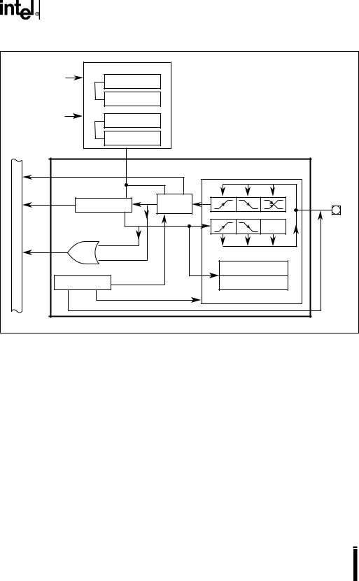
Each EPA channel has a control register, EPAx_CON; an event-time register, EPAx_TIME; and a timer/counter input (Figure 11-4). The control register selects the timer, the mode, and either the event that causes a timer/counter value to be captured or the event that is to occur at a given timer/counter value. The event-time register holds the captured timer value in capture mode or the event time in compare mode. See “Programming the Timers” on page 11-15 for configuration information.
11-9

8XC196EA USER’S MANUAL |
|
|
||
External Clocking |
|
Timer/Counter Unit |
|
|
|
|
|
|
|
(TxCLK) |
|
TIMER4 |
|
|
|
|
TIMER3 |
|
|
Internal Clocking |
|
TIMER2 |
|
|
|
|
|
|
|
|
|
TIMER1 |
|
|
|
|
|
|
EPA Capture/Compare |
|
|
Capture Overrun |
Channel x |
|
OVRx |
|
|
|
|
Interrupt |
|
|
Capture |
EPA Pin |
|
EPAx_TIME |
|||
|
Buffer |
|
||
|
|
|
|
|
|
|
|
Compare |
TGL |
Bus |
|
|
|
|
|
|
|
|
|
EPA |
|
|
|
|
Interrupt |
|
|
|
Reset Timer |
|
EPAx_CON |
Overwrite |
|
Start A/D |
|
|
|
||
|
|
Mode Control |
Mode Selection |
|
|
|
Concatenate |
|
|
|
|
|
|
A4330-01 |
|
Figure 11-4. A Single EPA Capture/Compare Channel |
11.4.1 Operating in Input Capture Mode
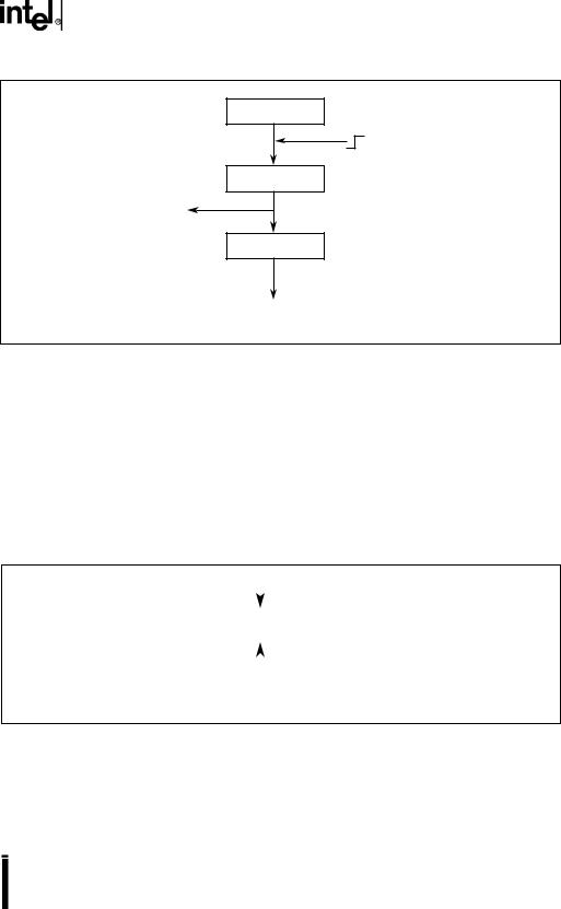
In capture mode, when a valid event occurs on the pin, the value of the selected timer is captured into a buffer. The timer value is then transferred from the buffer to the EPAx_TIME register, which sets the EPA interrupt pending bit as shown in Figure 11-5. If enabled, an interrupt is generated. If a second event occurs before the CPU reads the first timer value in EPAx_TIME, the second timer value is loaded into the buffer and held there. After the CPU reads the EPAx_TIME register, the value from the capture buffer is automatically transferred into EPAx_TIME and the EPA interrupt pending bit is set again.
11-10

EVENT PROCESSOR ARRAY (EPA)
TIMERx
Event Occurs
at EPA Pin
Capture Buffer
EPA
Interrupt
Pending Bit
Set
EPAx_TIME
Read-out Time Value
A2458-02
Figure 11-5. EPA Simplified Input Capture Structure
If a third event occurs before the CPU reads the event-time register, the overwrite bit (EPAx_CON.1) determines how the EPA will handle the event. If the bit is clear, the EPA ignores the third event. If the bit is set, the third event time overwrites the second event time in the capture buffer. Table 11-3 summarizes the possible actions when a valid event occurs.
NOTE
For an event to be captured, the signal must be stable for at least two state times both before and after the transition occurs (Figure 11-6).
Event 1 |
|
|
|
|
|
|
|
|
|
||
|
|
|
|
|
|
|
2 State |
|
2 State |
|
|
|
|
|
|
||
|
Times |
|
Times |
|
|
|
|
|
|
||
Event 2 |
|
|
|
|
|
|
|
|
|
||
|
|
|
|
||
|
|
|
|
|
|
|
2 State |
|
2 State |
|
|
|
|
|
|
||
|
Times |
|
Times |
|
|
|
|
|
|
A3130-01
Figure 11-6. Valid EPA Input Events
11-11

8XC196EA USER’S MANUAL
|
Table 11-3. Action Taken When a Valid Edge Occurs |
||
Overwrite Bit |
Status of |
|
|
Capture Buffer |
Action Taken When a Valid Edge Occurs |
||
(EPAx_CON.1) |
|||
& EPAx_TIME |
|
||
|
|
||
|
|
|
|
0 |
empty |
Edge is captured and event time is loaded into the capture buffer and |
|
|
|
EPAx_TIME register. |
|
0 |
full |
New data is ignored — no capture, EPA interrupt, or transfer occurs. |
|
1 |
empty |
Edge is captured and event time is loaded into the capture buffer and |
|
|
|
EPAx_TIME register. |
|
1 |
full |
Old data is overwritten in the capture buffer. |
An input capture event does not set the interrupt pending bit until the captured time value actually moves from the capture buffer into the EPAx_TIME register. If the buffer contains data and the PTS is used to service the interrupts, then two PTS interrupt requests will occur almost back-to- back (that is, with one instruction executed between the interrupts).
11.4.2 Operating in Output Compare Mode
When the selected timer value matches the event-time value, the action specified in the control register occurs (i.e., no output occurs or the pin is set, cleared, or toggled, or an A/D conversion is initiated). If the re-enable bit (EPAx_CON.5) is set, the action reoccurs on every timer match. If the re-enable bit is cleared, the action does not reoccur until a new value is written to the eventtime register. See “Programming the Capture/Compare Channels” on page 11-19 for configuration information.
11.4.3 Operating in Compare Mode with the Output/Simulcapture Channels
When the selected timer value matches the event-time value, the action specified in the control register occurs (i.e., the pin is set, cleared, or toggled, or an A/D conversion is initiated, or the waveform generator is reloaded), and the value of the selected timer is captured. If the re-enable bit (OSx_CON.5) is set, the action reoccurs on every timer match. If the re-enable bit is cleared, the action does not reoccur until a new value is written to the event-time register. See “Programming the Timers” on page 11-15 and “Programming the Capture/Compare Channels” on page 11-19 for configuration information.
11.4.4 Generating a 32-bit Time Value
The 83C196EA’s EPA module enables you to concatenate a pair of timers and a pair of EPA channels to generate or capture a 32-bit time value. Figure 11-7 illustrates this configuration using timers 1 and 2 and EPA channels 1 and 0. You can use timers 3 and 4 and any pair of adjacent channels in this same manner.
11-12