
- •CONTENTS
- •FIGURES
- •TABLES
- •1.1 Manual Contents
- •1.2 Notational Conventions and Terminology
- •1.3 Related Documents
- •1.4 Application Support Services
- •2.1 Typical Applications
- •2.2 Microcontroller Features
- •2.3 Functional Overview
- •2.3.1 Core
- •2.3.1.3 Register File
- •2.3.2 Memory Controller
- •2.4 Internal Timing
- •2.4.1 Clock and Power Management Logic
- •2.4.2 Internal Timing
- •2.4.2.1 Clock Failure Detection Logic
- •2.4.2.2 External Timing
- •2.4.2.3 Power Management Options
- •2.4.3 Internal Memory
- •2.4.4 Serial Debug Unit
- •2.4.5 Interrupt Service
- •2.5 Internal Peripherals
- •2.5.1 I/O Ports
- •2.5.2 Serial I/O (SIO) Port
- •2.5.3 Synchronous Serial I/O (SSIO) Port
- •2.5.4 Event Processor Array (EPA) and Timer/Counters
- •2.5.7 Stack Overflow Module
- •2.5.8 Watchdog Timer
- •2.6 Special Operating Modes
- •2.7 Chip Configuration Registers
- •3.1 Overview of the Instruction Set
- •3.1.1 BIT Operands
- •3.1.2 BYTE Operands
- •3.1.4 WORD Operands
- •3.1.5 INTEGER Operands
- •3.1.9 Converting Operands
- •3.1.10 Conditional Jumps
- •3.1.11 Floating-Point Operations
- •3.1.12 Extended Instructions
- •3.2 Addressing Modes
- •3.2.1 Direct Addressing
- •3.2.2 Immediate Addressing
- •3.2.3 Indirect Addressing
- •3.2.3.1 Extended Indirect Addressing
- •3.2.3.2 Indirect Addressing with Autoincrement
- •3.2.3.3 Extended Indirect Addressing with Autoincrement
- •3.2.3.4 Indirect Addressing with the Stack Pointer
- •3.2.4 Indexed Addressing
- •3.2.4.3 Extended Indexed Addressing
- •3.2.4.4 Zero-indexed Addressing
- •3.3 Considerations for Crossing Page Boundaries
- •3.4 Software Protection Features and Guidelines
- •4.1 Memory Map Overview
- •4.2 Memory Partitions
- •4.2.1 External Memory
- •4.2.2 Internal ROM
- •4.2.2.1 Program Memory in Page FFH
- •4.2.2.3 Reserved Memory Locations
- •4.2.2.4 Interrupt, PIH, and PTS Vectors
- •4.2.2.5 Chip Configuration Bytes
- •4.2.3 Internal RAM (Code RAM)
- •4.2.4.2 Peripheral SFRs
- •4.2.5 Register File
- •4.2.5.2 Stack Pointer (SP)
- •4.3 Windowing
- •4.3.1 Selecting a Window
- •4.3.2 Addressing a Location Through a Window
- •4.3.2.4 Unsupported Locations Windowing Example
- •4.3.2.5 Using the Linker Locator to Set Up a Window
- •4.3.3 Windowing and Addressing Modes
- •4.4 Controlling Read Access to the Internal ROM
- •4.5 Remapping Internal ROM
- •5.1 Functional Overview
- •5.2 Stack Operations
- •5.3 Stack Overflow Module Registers
- •5.4 Programming the Stack Overflow Module
- •5.4.1 Initializing the Stack Pointer
- •5.4.2 Enabling the Stack Overflow Module and Specifying Stack Boundaries
- •6.1 Overview of the Interrupt Control Circuitry
- •6.2 Interrupt Signals and Registers
- •6.3 Interrupt Sources, Priorities, and Vector Addresses
- •6.3.1 PIH Interrupt Sources, Priorities, and Vector Addresses
- •6.3.1.1 Using Software to Provide the Vector Address
- •6.3.1.2 Providing the Vector Address in Response to a CPU Request
- •6.3.2 Special Interrupts
- •6.3.2.1 Unimplemented Opcode
- •6.3.2.2 Software Trap
- •6.3.2.4 Stack Overflow
- •6.3.3 External Interrupt Signal
- •6.3.4 Shared Interrupt Requests
- •6.4 Interrupt Latency
- •6.4.1 Situations that Increase Interrupt Latency
- •6.4.2 Calculating Latency
- •6.4.2.2 PTS Interrupt Latency
- •6.5 Programming the Interrupts
- •6.5.1 Modifying Interrupt Priorities
- •6.5.2 Determining the Source of an Interrupt
- •6.6 Initializing the PTS Control Blocks
- •6.6.1 Specifying the PTS Count
- •6.6.2 Selecting the PTS Mode
- •6.6.3 Single Transfer Mode
- •6.6.4 Block Transfer Mode
- •6.6.5 Dummy Mode
- •7.1 I/O Ports Overview
- •7.2 Configuring the Port Pins
- •7.2.2 Configuring Ports 3 and 4 (Address/Data Bus)
- •7.2.3 Port Configuration Example
- •7.3.1 Address and Data Signals (Ports 3, 4, and EPORT)
- •7.3.1.1 EPORT Status During Reset, CCB Fetch, Idle, Powerdown, and Hold
- •7.3.5 External Interrupt Signal (Port 2)
- •7.3.6 PWM Signals (Port 11)
- •7.3.7 Serial I/O Port Signals (Ports 2 and 7)
- •7.3.8 Special Operating Mode Signal (Port 5 Pin 7)
- •7.3.9 Synchronous Serial I/O Port Signals (Port 10)
- •7.4 I/O Port Internal Structures
- •7.4.3 Internal Structure for Ports 3 and 4 (Address/Data Bus)
- •8.1 Serial I/O (SIO) Port Functional Overview
- •8.2 Serial I/O Port Signals and Registers
- •8.3 Serial Port Modes
- •8.3.1 Synchronous Mode (Mode 0)
- •8.3.2 Asynchronous Modes (Modes 1, 2, and 3)
- •8.3.2.1 Mode 1
- •8.3.2.2 Mode 2
- •8.3.2.3 Mode 3
- •8.3.2.4 Multiprocessor Communications
- •8.4 Programming the Serial Port
- •8.4.1 Configuring the Serial Port Pins
- •8.4.2 Programming the Control Register
- •8.4.3 Programming the Baud Rate and Clock Source
- •8.4.4 Enabling the Serial Port Interrupts
- •8.4.5 Determining Serial Port Status
- •CHAPTER 9 Synchronous Serial I/O (SSIO) Port
- •9.1 SSIO Port Overview
- •9.1.1 Standard Mode
- •9.1.2 Duplex Mode
- •9.2 SSIO pORT sIGNALS AND rEGISTERS
- •9.3 ssio Port Operation
- •9.3.1 Transmitting and Receiving Data
- •9.3.1.1 Normal Transfers (All Modes)
- •9.3.1.2 Handshaking Transfers (Standard Mode Only)
- •9.4 Programming the SSIO Port
- •9.4.1 Configuring the SSIO Port Pins
- •9.4.2 Configuring the SSIO Registers
- •9.4.2.1 The SSIO Baud (SSIO_BAUD) Register
- •9.4.2.3 The SSIO 0 Clock (SSIO0_CLK) Register
- •9.4.2.4 The SSIO 1 Clock (SSIO1_CLK) Register
- •9.4.3 Enabling the SSIO Interrupts
- •9.5 Programming Considerations
- •9.5.2 Standard Mode Considerations
- •9.5.3 Duplex Mode Considerations
- •10.1 PWM FUNCTIONAL OVERVIEW
- •10.2 PWM Signals and Registers
- •10.3 pwm operation
- •10.4 Programming the Frequency and Period
- •10.5 Programming the Duty Cycle
- •10.5.1 Sample Calculations
- •10.5.2 Reading the Current Value of the Down-counter
- •10.5.3 Enabling the PWM Outputs
- •10.5.4 Generating Analog Outputs
- •11.1 EPA Functional Overview
- •11.2 EPA and Timer/Counter Signals and Registers
- •11.3 Timer/Counter Functional Overview
- •11.3.1 Timer Multiplexing on the Time Bus
- •11.4 EPA Channel Functional Overview
- •11.4.1 Operating in Input Capture Mode
- •11.4.2 Operating in Output Compare Mode
- •11.4.3 Operating in Compare Mode with the Output/Simulcapture Channels
- •11.4.4 Generating a 32-bit Time Value
- •11.4.5 Controlling a Pair of Adjacent Pins
- •11.5 Programming the EPA and Timer/Counters
- •11.5.1 Configuring the EPA and Timer/Counter Signals
- •11.5.2 Programming the Timers
- •11.5.3 Programming the Capture/Compare Channels
- •11.5.4 Programming the Compare-only (Output/Simulcapture) Channels
- •11.6 Enabling the EPA Interrupts
- •11.7 Determining Event Status
- •CHAPTER 12 Analog-to-digital (A/D) Converter
- •12.1 A/D Converter Functional Overview
- •12.2 A/D Converter Signals and Registers
- •12.3 A/D Converter Operation
- •12.4 Programming the A/D Converter
- •12.4.1 Programming the A/D Test Register
- •12.4.2 Programming the A/D Result Register (for Threshold Detection Only)
- •12.4.3 Programming the A/D Time Register
- •12.4.4 Programming the A/D Command Register
- •12.4.5 Programming the A/D Scan Register
- •12.4.6 Enabling the A/D Interrupt
- •12.5 Determining A/D Status and Conversion Results
- •12.6 Design Considerations
- •12.6.1 Designing External Interface Circuitry
- •12.6.1.1 Minimizing the Effect of High Input Source Resistance
- •12.6.1.2 Suggested A/D Input Circuit
- •12.6.1.3 Analog Ground and Reference Voltages
- •12.6.2 Understanding A/D Conversion Errors
- •CHAPTER 13 Minimum Hardware Considerations
- •13.1 Minimum Connections
- •13.1.1 Unused Inputs
- •13.1.2 I/O Port Pin Connections
- •13.2 Applying and Removing Power
- •13.3 Noise Protection Tips
- •13.4 The On-chip Oscillator Circuitry
- •13.5 Using an External Clock Source
- •13.6 Resetting the Microcontroller
- •13.6.1 Generating an External Reset
- •13.6.2 Issuing the Reset (RST) Instruction
- •13.6.3 Issuing an Illegal IDLPD Key Operand
- •13.6.4 Enabling the Watchdog Timer
- •13.6.5 Detecting Clock Failure
- •13.7 Identifying the Reset Source
- •14.1 Special Operating Mode Signals and Registers
- •14.2 Reducing Power Consumption
- •14.3 Idle Mode
- •14.3.1 Enabling and Disabling Idle Mode
- •14.3.2 Entering and Exiting Idle Mode
- •14.4 Powerdown Mode
- •14.4.1 Enabling and Disabling Powerdown Mode
- •14.4.2 Entering Powerdown Mode
- •14.4.3 Exiting Powerdown Mode
- •14.4.3.1 Generating a Hardware Reset
- •14.4.3.2 Asserting the External Interrupt Signal
- •14.4.3.3 Selecting an External Capacitor
- •14.5 ONCE Mode
- •CHAPTER 15 Interfacing with External Memory
- •15.1 Internal and External Addresses
- •15.2 External Memory Interface Signals and Registers
- •15.3 The Chip-select Unit
- •15.3.1 Defining Chip-select Address Ranges
- •15.3.2 Controlling Bus Parameters
- •15.3.3 Chip-select Unit Initial Conditions
- •15.3.4 Programming the Chip-select Registers
- •15.3.5 Example of a Chip-select Setup
- •15.4 Chip Configuration Registers and Chip Configuration Bytes
- •15.5 Bus Width and Multiplexing
- •15.5.1 A 16-bit Example System
- •15.5.2 16-bit Bus Timings
- •15.5.3 8-bit Bus Timings
- •15.5.4 Comparison of Multiplexed and Demultiplexed Buses
- •15.6 Wait States (Ready Control)
- •15.7 Bus-hold Protocol
- •15.7.1 Enabling the Bus-hold Protocol
- •15.7.2 Disabling the Bus-hold Protocol
- •15.7.3 Hold Latency
- •15.7.4 Regaining Bus Control
- •15.8 Write-control Modes
- •15.9 System Bus AC Timing Specifications
- •15.9.1 Deferred Bus-cycle Mode
- •15.9.2 Explanation of AC Symbols
- •15.9.3 AC Timing Definitions
- •16.1 Serial Debug Unit (SDU) Functional Overview
- •16.2 SDU Signals and Registers
- •16.3 SDU Operation
- •16.3.1 SDU State Machine
- •16.3.2 Code RAM Access State Machine
- •16.3.3 Minimizing Latency
- •16.4 Code RAM Access
- •16.4.1 Code RAM Data Transfer
- •16.4.2 Code RAM Access Instructions
- •16.4.3 Code RAM Data Transfer Example
- •16.5 SDU Interface Connector
- •17.1 Signals and Registers
- •17.2 Memory Protection Options
- •17.3 Entering Test-ROM Routines
- •17.3.1 Power-up and Power-down Sequences
- •17.4 ROM-dump Routine and Circuit
- •17.5 Serial Port Mode Routine
- •17.5.1 Serial Port RISM
- •17.5.2 Serial Port Mode Circuit
- •17.6 SDU RISM Execution Routine
- •17.6.1 SDU RISM Data Transfer
- •17.6.1.1 SDU RISM Data Transfer Before
- •17.6.1.2 SDU RISM Data Transfer After
- •17.6.2 SDU RISM Execution Circuit
- •17.7 RISM Command Descriptions
- •17.8 Executing Programs from Register RAM
- •17.9 RISM Command Examples
- •17.9.1 Serial Port Mode RISM Read Command Example
- •17.9.2 Serial Port Mode RISM Write Command Example
- •17.9.3 SDU RISM Execution Write Command Example
- •17.9.4 SDU RISM Execution Go Command Example
- •B.1 Functional Groupings of Signals
- •B.2 Signal Descriptions
- •B.3 Default Conditions

CHAPTER 9 SYNCHRONOUS SERIAL I/O (SSIO) PORT
This device has a synchronous serial I/O (SSIO) port that shares pins with port 10. The SSIO provides two unidirectional serial communication channels or one synchronous bidirectional communication channel. The SSIO is compatible with most protocols because the serial clock is completely configurable. Paired, the SSIO channels can operate in a channel-select mode, allowing for communication in multiple-master systems without additional external hardware. Each SSIO channel can also perform handshaking transfers, which along with the PTS, provides unidirectional, multi-byte transfers with no CPU overhead. This chapter describes the SSIO port and explains how to program it.
9.1SSIO PORT OVERVIEW
The SSIO port has three modes of operation: standard, duplex, and channel-select. For singleslave, single-master systems requiring only one SSIO channel or two independent SSIO channels, use the standard mode of operation. In standard mode, each channel has a unique serial clock and data signal. For single-slave, single-master systems requiring two SSIO channels, use the duplex mode of operation. In duplex mode, the channels have unique serial data signals, but share a common clock signal. For systems with multiple masters or multiple slaves, use the channel-select mode of operation. Like duplex mode, in channel-select mode, the channels have unique serial data signals, but share a common clock signal. Channel-select mode provides an additional chan- nel-select signal designed for communicating in systems with multiple masters or multiple slaves.
In addition to three operating modes, the SSIO port can perform two types of data transfers: normal and handshaking. All modes support normal transfers, while only standard mode supports handshaking transfers. Normal transfers are compatible with most protocols because the serial clock is completely configurable. Handshaking transfers allow a slave device to notify the master that it is not ready for a transfer. “Normal Transfers (All Modes)” on page 9-9 and “Handshaking Transfers (Standard Mode Only)” on page 9-10 discuss these transfer types in detail.
9.1.1Standard Mode
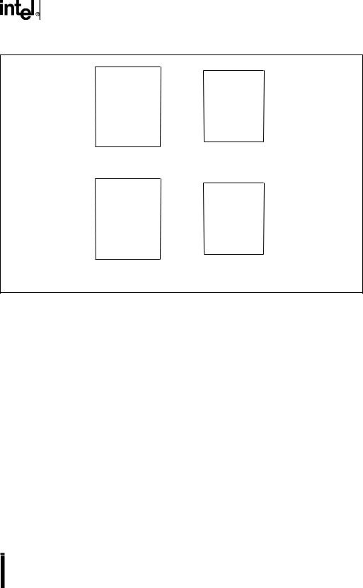
In standard mode, the SSIO channels operate as two independent serial channels. Each channel contains one clock signal and one data signal. This mode is useful for systems in which unidirectional or half-duplex communication is acceptable. Half-duplex communication uses the same data signal for both transmissions and receptions. In standard mode, the channels can act as either master or slave and as either transmitter or receiver, resulting in the four configuration options shown in Figure 9-1.
9-1

8XC196EA USER’S MANUAL
Microcontroller |
|
|
|
|
|
Microcontroller |
|
|
|
|
|
|
|
|
|
|
|
|
|
|
|
|
|
|
|
Peripheral |
|
|
|
|
|
Peripheral |
SCx |
|
|
|
Clock |
|
SCx |
|
|
|
Clock |
|
|
|
|
|
|
|
||||
SDx |
|
|
|
Data Out |
|
SDx |
|
|
|
Data In |
|
|
|
|
|
|
|
||||
Master |
|
|
|
Slave |
|
Master |
|
|
|
Slave |
|
|
|
|
|
|
|
|
|
|
|
|
|
|
|
|
|
|
|
|
|
|
Master Receiver |
|
Master Transmitter |
||||||||
|
|
|
|
|
|
|
|
|
||
Microcontroller |
|
|
|
|
|
Microcontroller |
|
|
|
|
|
|
|
|
|
|
|
|
|
|
|
|
|
|
|
Peripheral |
|
|
|
|
|
Peripheral |
SCx |
|
|
|
Clock |
|
SCx |
|
|
|
Clock |
|
|
|
|
|
|
|
||||
SDx |
|
|
|
Data Out |
|
SDx |
|
|
|
Data In |
|
|
|
|
|
|
|
||||
Slave |
|
|
|
Master |
|
Slave |
|
|
|
Master |
|
|
|
|
|
|
|
|
|
|
|
|
|
|
|
|
|
|
|
|
||
Slave Receiver |
|
Slave Transmitter |
A3306-01
Figure 9-1. Standard Mode Configuration Options
A master device generates a clocking signal and a slave device receives a clock signal. As shown in Figure 9-1, with a master configuration, the SSIO channel outputs a clocking signal on its serial clock (SCx) pin. With a slave configuration, the clocking signal is input on SCx. When the channel acts as a receiver, the SSIO port shifts an 8-bit data stream (MSB first) into the microcontroller through its serial data (SDx) pin. When the channel acts as a transmitter, the SSIO port shifts data out of the microcontroller through SDx.
9.1.2Duplex Mode
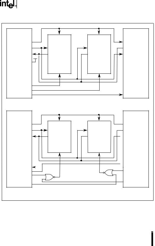
In duplex mode, the SSIO channels operate as a pair to provide full-duplex communication. Fullduplex communication uses separate data signals for receptions and transmissions. In this mode, the SSIO can act as either master or slave, and it transmits data through its serial data 0 (SD0) signal and receives data through its serial data 1 (SD1) signal. As master, the SSIO outputs a clocking signal on its serial clock (SC0) pin. As slave, the SSIO receives an externally generated clocking signal on SC0. Figure 9-2 shows the duplex-mode configuration options.
9-2

SYNCHRONOUS SERIAL I/O (SSIO) PORT
Microcontroller
Peripheral
SC0 Clock
SD0 Data In
SD1 Data Out
Master |
Slave |
|
Microcontroller as Master
Microcontroller
Peripheral
SC0 Clock
SD0 Data In
SD1 Data Out
Slave |
Master |
|
Microcontroller as Slave
A3312-01
Figure 9-2. Duplex Mode Configuration Options
9.1.3Channel-select Mode
In channel-select mode, the SSIO channels operate as one serial channel for communications in systems with multiple slaves or multiple masters. With this configuration, the SSIO can act as either master or slave. Channel-select mode uses four signals: two serial data signals (SD0 and SD1), a clock signal (SC0), and a channel-select signal (CHS#). In channel-select mode, the SSIO can provide full-duplex communication, using both SD0 and SD1 data signals, or it can provide half-duplex communication, using only the SD1 data signal. When the SSIO is configured as a slave, an external master activates CHS# to communicate with the SSIO. When the SSIO is configured as a master, an external master activates CHS# when it wants the SSIO to give up the bus. When the microcontroller is the only master in a system, tie the CHS# signal high because the SSIO does not need to relinquish the bus to another master. Figure 9-3 shows channel-select configurations.
9-3

8XC196EA USER’S MANUAL
Microcontroller 1 |
|
|
Microcontroller 2 |
(master) |
Clock |
Clock |
(slave) |
|
|
||
SC0 |
|
|
SC0 |
SD0 |
Data In |
Data In |
SD0 |
SD1 |
Data Out |
Data Out |
SD1 |
CHS# |
Peripheral 1 |
Peripheral 2 |
|
(slave) |
(slave) |
|
|
|
CS# |
CS# |
|
Pn.x |
|
|
|
Pn.y |
|
|
|
Pn.z |
|
|
CHS# |
System with Multiple Slaves
Microcontroller 1 |
|
|
(master) |
|
|
SC0 |
Clock |
Clock |
SD0 |
Data In |
Data In |
SD1 |
Data Out |
Data Out |
|
Peripheral 1 |
Peripheral 2 |
|
(slave) |
(slave) |
|
CS# |
CS# |
CHS# |
|
|
Px.1 |
|
|
Px.2 |
|
|
Px.3 |
|
|
Microcontroller 2
(master)
SC0
SD0
SD1
CHS#
Px.1
Px.3
Px.2
System with Multiple Masters
A3354-01
Figure 9-3. Channel-select Configuration Options
9-4